27 minute read
Realising red microLEDs with europium-doping


Realising red GaN-based microLEDs with europium-doping
The novel red luminescence provided by doping GaN with europium ions enables the monolithic integration of nitride-based full-colour LEDs for ultrahigh-resolution microLED displays BY SHUHEI ICHIKAWA, DOLF TIMMERMAN, JUN TATEBAYASHI AND YASUFUMI FUJIWARA FROM OSAKA UNIVERSITY
Advertisement
WE ARE ON THE CUSP of a new era, known as ‘Smart society’, that will see cyber space and the physical space interactively fused. Critical to this is the introduction of a small-size, high-resolution display, which is an essential ingredient in virtual-reality, augmented-reality and mixed-reality glasses.
One candidate for producing these tiny highresolution displays is the microLED. Screens formed from a vast array of these miniature LEDs have many virtues, including a high efficiency, high contrast and high stability. Fabrication of this class of display draws together devices emitting each of the three primary colours. A very common combination is the use of InGaN/GaN-based LEDs for the blue and green and AlInGaP/GaAs-based LEDs for the red. These devices are brought together to form pixels using a pick-andplace technique. However, there is a problem: when the dimensions of the LEDs are reduced, the efficiency of the red variant plummets, due to an increase in
surface recombination associated with the hike in the surface-to-volume ratio.
Several solutions are being explored for reducing the dimensions of the red LED while maintaining its efficiency. One option, receiving much attention, is to use GaN-based LEDs emitting in the blue or ultraviolet to pump red-emitting quantum dots or phosphors. However, while this approach also offers monolithic integration, it suffers from insufficient stability and an inadequate colour-conversion efficiency. What’s more, with this particular technology, there is a need to increase the pixel contrast ratio and enhance the colour purity by suppressing crosstalk between various light emitters. Unfortunately, when black light-blocking partitions are applied between all the subpixels to accomplish this, the effective area of the pixels diminishes, impairing the number of pixels-perinch (PPI).
Switching to InGaN nanocolumns avoids this issue. It’s an architecture that effectively relaxes material strain, even for the high-indium contents that are necessary for red light emission. But it is challenging to produce nanocolumn structures with a high colour purity – they are held back by large variations in emission wavelength, due to the ensemble nature of these structures and the sensitivity of individual nanocolumns to size fluctuations. Another drawback is the need for electron-beam lithography, prior to epitaxial growth, to precisely control the nanocolumn size and ultimately ensure the desired emission wavelength. Note that for this type of microLED, and also for that based on quantum dots, fabrication requires a lateral integration method.
There is much merit in taking a very different approach, based on the vertical-stacking integration of tri-colour LEDs. Realising this with a single epitaxial sequence eradicates several steps in the microLED production process, such as the mask-patterning prior to growth and the addition of black partitions. What’s more, with this technique the areal density of the microLEDs is only limited by lithography and flip-chip accuracy, so it is possible to integrate these emitters with a PPI beyond 5,000.
A pioneer of this approach is the group led by the Nobel-prize winning physicist Hirsohi Amano. Recently his team demonstrated the monolithic integration of tri-colour microLEDs using InGaN quantum wells. These devices, with a 100 μm by 100 μm active area, are composed of independent subpixels, which emit in the blue, green and yellow–orange range and have a colour saturation of over 90 percent. However, there are drawbacks: one concern is that the longer wavelength emission is much broader; and another is that its peak position shifts to shorter wavelengths as the injected current increases, due to a reduction in the quantum-confined Stark effect.
Our team offers a way to overcome this issue, drawing on our previous success from more than a decade ago. Back in 2009 we invented a novel red LED, formed by adopting europium-doped GaN. In the intervening years we have continued to refine this device, enabling its output power to steadily increase to the milliwatt level. In the remainder of this feature we will detail this triumph, and how we have used vertically-stacked integration to combine it with conventional blue/green LEDs to create a
Figure 2. Eu3+ ions doped in GaN under current injection deliver a very sharp emission peak, crucial for a high colour purity. Figure 1. Europiumdoped GaN LED arrays exhibit bright red luminescence.
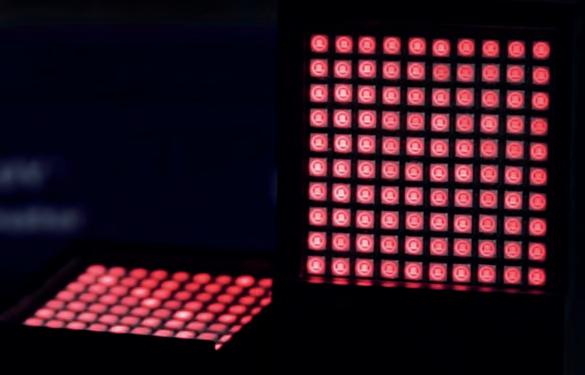
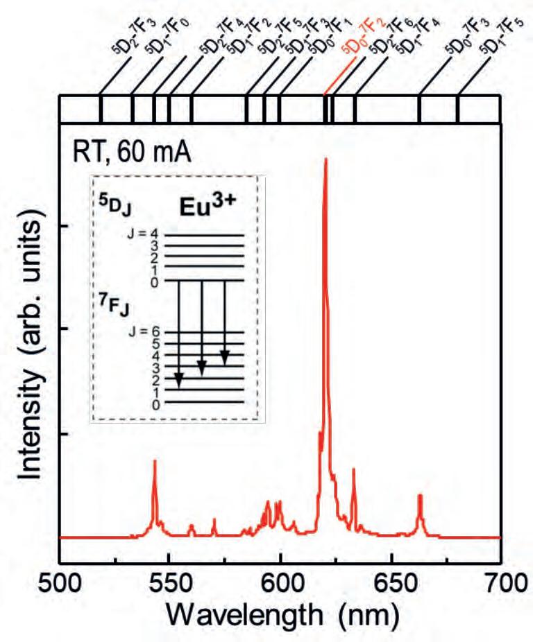
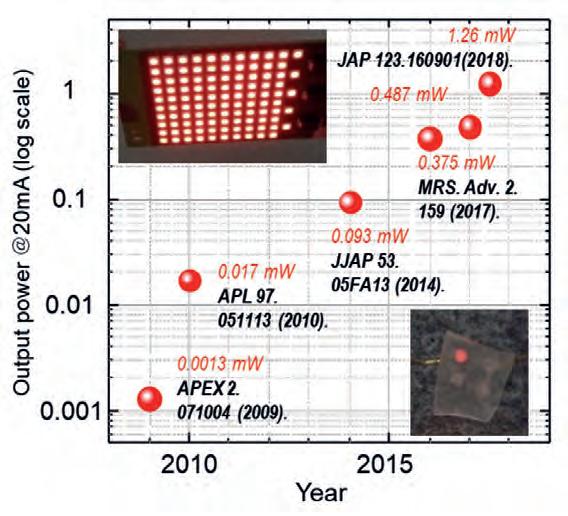
Figure 3. Recent progress of the output power of europium-doped GaN-based LEDs produced at Osaka University. key technology for the next-generation of microLED displays.
Europium doping
Our approach fulfils the requirement for the verticalstacking of tri-colour LEDs, which is the monolithic integration of all three colours. We needed to develop and alternative to the more obvious approach of just using InGaN quantum wells, because although blue and green LEDs based on this have been successfully commercialized, a red cousin is lacking. The route to producing red emission with this type of LED is to either increase the indium-content or the thickness of the InGaN quantum well, or to use a combination of the two. But this strategy is precarious: it leads to an increase in piezo-electric polarization fields, and the low miscibility of indium in GaN hampers efforts to realise a sufficient indium content in the well while maintaining sufficient crystal quality. We are able to sidestep these issues by manipulating the emission through the doping of GaN with an intrinsic red emitter, the rare-earth element europium Eu3+ .
The Eu3+ ion is no stranger to display applications, having been widely deployed as a luminescent centre in red-emitting phosphors in cathode ray tubes and plasma display panels. In general, rare-earth ions, including Eu3+, are characterized by partially filled 4f shells, which are localized inside completely filled 5s and 5p shells. This localization shields the electrons in the 4f shell from the surrounding environment, allowing rare-earth ions to maintain their atom-like properties and exhibit sharp luminescence bands associated with radiative transitions within the 4f manifold. These transitions are virtually insensitive to changes in current injection and temperature. When Eu3+ ions are incorporated into GaN, they take the place of the Ga3+ metallic cations and occupy sites with reduced symmetry.
Adding Eu3+ ions alters the light-emitting mechanism. Conventional band-to-band transitions are replaced by the transfer of energy from injected carriers in the GaN host material to Eu3+ ions, which are promoted to an excited state that leads to the emission of red light. This energy transfer is strongly dependent on the material properties, and can be enhanced by changing the material fabrication processes, or by intentionally introducing other dopants, which can act as energy hubs.
Eu3+ ions exhibit a sharp luminescence around 620 nm, due to intra-4f shell transitions from the 5D0 to 7F2 states (see Figure 2). This attribute is most welcome, helping to create red-emitting devices with a high colour purity and robust emission wavelength stability. Over the last decade and more, we have developed expertise to epitaxially grow high-quality GaN materials that are doped with Eu3+ ions and are optimised to deliver excellent performance in LED structures. The output power of these devices has exponentially increased over time, and has recently exceeded 1 mW at 20 mA, a respectable figure for mass production (see Figure 3).
Maintaining efficiency
To enable immersive experiences in entertainment, education and communication, microdisplays need to come as close as possible to matching the human visual system. For a typical virtual-reality headset, this requirement implies that the spatial resolution needs to be as high as 4600 PPI to match the eye’s central field-of-view capabilities. This specification translates to a pixel size of approximately 5 μm, and thus even smaller feature sizes for individual sub-pixels.
When the dimensions of a microLED are reduced to below around 100 μm, the influence of their sidewalls increases, leading to the introduction of non-radiative recombination associated with imperfections induced
by the fabrication process. The upshot is a lowering of the internal conversion efficiency. To address this, engineers are turning to new LED structures, modified chip architectures and better processes to diminish the impact of sidewall defects. With these refinements, blue-emitting microLEDs based on InGaN quantum wells can maintain their efficiency when scaled down to a size of just 5 μm.
With red microLEDs, which are typically based on phosphides, it’s a different story. The issues associated with scaling are not addressed with the approaches that work for their GaN-based siblings, and their efficiency drops quickly when the pixel size shrinks. These devices are hampered by a combination of long carrier diffusion lengths that allow carriers to reach sidewalls from a larger distance, and the high surface-recombination coefficient.
When switching from red LEDs made from phosphides to those employing europium-doped GaN, the carrier diffusion length plummets to a value even shorter than that found in conventional nitrides. That’s because the Eu3+ ions are extremely efficient at trapping injected carriers. Diffusion lengths are typically around 100 nm, a distance so small that carriers are prevented from reaching the sidewalls.
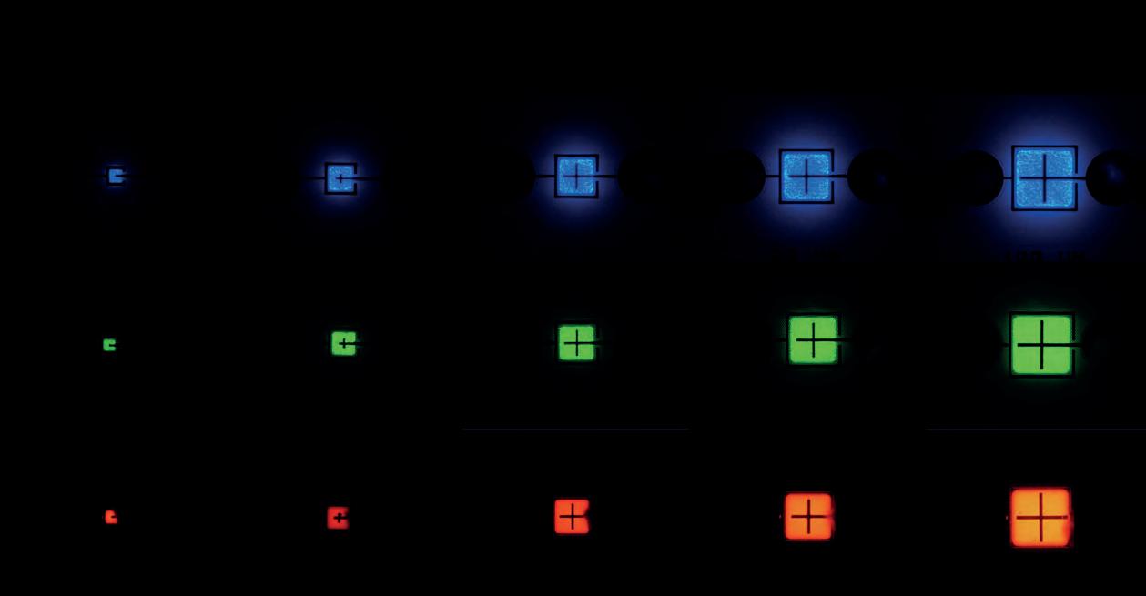
This virtue is at play in our set of square europiumdoped structures, with sizes ranging from 1 μm to 100 μm (see Figure 5). We have found that the internal quantum efficiency remains constant down to sizes of 10 μm, and only shows modest decreases at even smaller sizes. For our smallest structure of 1 μm, the internal quantum efficiency is 70 percent of the maximum value. This impressive result is realised without any post-treatment of the sidewalls, so it could be further improved by employing the process optimizations developed for the blue GaN-based LEDs.
Our results underscore the inherent potential of europium-doped GaN as an optically active material, and they provide much encouragement for using this material in microLEDs. The work has provided us with a platform to investigate the performance of microLED structures based on this material. We hope that we can realise high efficiencies in devices as small as 1 μm.
Monolithic integration
Compared with displays based on conventional liquid crystals and organic LEDs, those employing microLEDs offer an increased pixel density, a higher efficiency and a hike in brightness. However, commercialising this technology in its highest fidelity is not easy, due to complexity in the fabrication of high-resolution full-colour displays that provide a wide colour gamut.
To realize a pixel density beyond 1000 PPI, it is indispensable to employ a growth technique that allows the monolithic integration of the three primarycolour LEDs from the same material system, because this eliminates complications arising from pick-andplace techniques used to transfer ultra-small-sized LED chips. For ultra-high resolutions beyond 4600 PPI, it is also advantageous to adopt a vertical stacking approach for bringing together red, green and blue LEDs, because this minimises gaps between pixels and sub-pixels. Another consideration is to realise a luminance of at least 3,000 cd m-2, as this
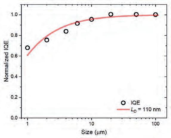
Figure 5. Normalized internal quantum efficiency as a function of mesa size for europium-doped GaN-based LEDs. The red line indicates the modelled internal quantum efficiency for a 110 nm carrier diffusion length.
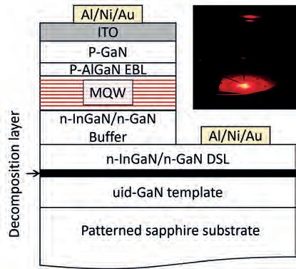
Figure 6. Vertical stacking of red, green and blue LEDs enables a very high pixel density (left). Electroluminescence from monolithically integrated LEDs on the same sapphire substrate under simultaneous operating conditions (right).
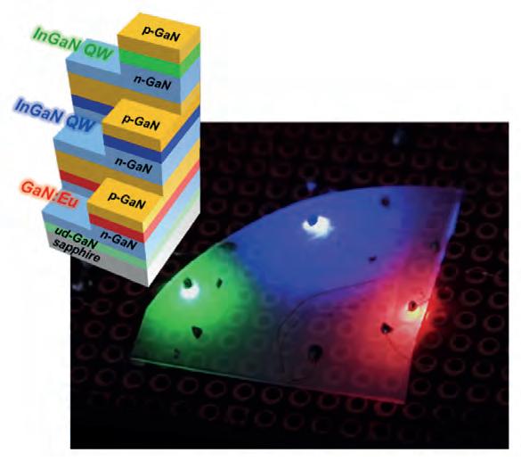
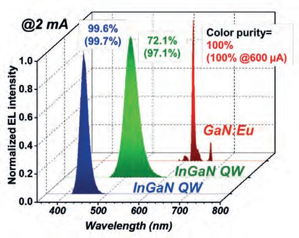
Figure 7. Individual electroluminescence spectra of red, green and blue LEDs obtained at room temperature under 2 mA current injection.
allows displays to be read outdoors, assuming a typical ambient illuminance of 50,000 lux.
Accounting for all these considerations, we have used monolithic integration to produce vertically stacked full-colour LEDs that feature europium-doped GaN and the emission from InGaN quantum wells (see Figure 6). These integrated LEDs were grown by MOCVD on a single sapphire substrate and did not require any additional preparation. It is possible to select all three primary colours from anywhere in the wafer by controlling the etching-depth and position.
The optimal growth temperature for the europiumdoped GaN layer is 960 °C – this is higher than that used for the InGaN quantum wells, which are grown at temperatures between 650 °C and 800 °C.
The europium-doped layer is thermally stable at the temperature employed for its growth, and is better suited for stacked-type integration of red, green and blue devices than InGaN-based red LEDs, which suffer from indium desorption. This desorption is accelerated by temperatures used for the growth of the InGaN layers used in subsequent LEDs.
Room-temperature electroluminescence spectra of our individual devices show a high colour purity. This is valued, as it improves the capability for displays to generate reproducible colours. Driven with a 600 μA injection current, the maximum colour purity for the red, green, and blue emission are 100 percent, 97.1 percent, and 99.7 percent, respectively (these figures are 100 percent, 72.1 percent, and 99.6 percent, respectively, at 2 mA operation). These results demonstrate the extremely high colour purity of europium-doped GaN LEDs under any current injection, due to the stable intra-4f shell transitions in the Eu3+ ions.
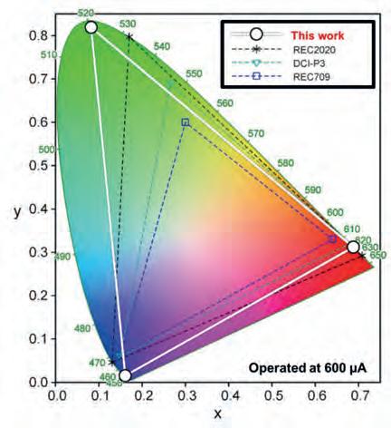
The most common approach to evaluating the reproducibility of colours of displays is to consider the space on the International Commission on Illumination (CIE) chromaticity diagram (see Figure 8). Using this metric – and the colour purity efficiencies for our red, green and blue LEDs – indicates that this combination of emitters provides an exceptionally large coverage. According to the Rec.2020 standard, our devices provide 105.5 percent of the area with 91.2 percent coverage; and for the DCI-P3 standard, the corresponding values are 147.0 percent and 96.5 percent, respectively. Crucially, these figures show that our devices fulfil the colour gamut requirement for the Ultra HD Premium TV standard. What’s more, they produce a maximum luminance of around 3100 cd m-2, so they satisfy the minimum requirement for outdoor applications.
These results show that our technology has a great deal of promise. By adding europium doping to the microLED to aid monolithic integration, we are paving the way for displays with a very high PPI and great colour quality that can serve in virtual-reality, augmented-reality and mixed-reality glasses.
FURTHER READING
A. Nishikawa et al. Appl. Phys. Express 2 071004 (2009) S. Ichikawa et al. Appl. Phys. Express 14 031008 (2021) D. D. van der Gon et al. Opt. Lett. 45 3973 (2020) B. Mitchell et al J. Appl. Phys. 123 160901 (2018) Figure 8. The emission colour gamut of red, green and blue LEDs on the CIE chromaticity diagram under 600 μA current injection.
PROCESS APPLICATION
• Ion Implantation • Plasma Etch • Chamber Clean • Photovoltaics • HDP-CVD • LPCVD • PECVD • MOCVD • ALD


CLEANSORB®
Point-of-exhaust absorption for process waste gas
CLEAN-PROTECT
Removal of toxic gases during emergency leakage in gas cabinets
CLEANVENT
Removal of hazardous gases during purging of vent lines
RZ_Anzeige CS Clean 1/2, 2020.indd 1

EXHAUST GAS TREATMENT
CLEANSORB® Dry Bed Abatement
Safe, dry chemical conversion of hazardous gases to stable solids Proprietary CLEANSORB® media No handling of toxic waste Practically maintenance-free Local Refill service worldwide
www.csclean.com
07.12.20 14:20
CS ONLINE ROUNDTABLE
BASED around a hot industry topic for your company, this 60-minute recorded, moderated zoom roundtable would be a platform for debate and discussion. MODERATED by an editor, this online event would include 3 speakers, with questions prepared and shared in advance. THIS ONLINE EVENT would be publicised for 4 weeks pre and 4 weeks post through all our mediums and become a valuable educational asset for your company

Contact: Jackie.cannon@angelbc.com
Cranking up the growth temperature of red InGaN LEDs
Intentional decomposition of an InGaN layer provides a foundation for high-temperature growth of red-emitting quantum wells
RESEARCHERS at the University of California, Santa Barbara (UCSB), claim to have broken new ground by increasing the temperature employed for the growth of red-emitting InGaN LEDs. This breakthrough comes from introducing a relaxed InGaN buffer.
The approach by the West-coast team differs from the norm, which is to grow re-emitting InGaN-based LEDs at a considerably lower temperatures than their green and blue siblings. While growth at a lower temperature enables the higher indium content in the quantum wells required for emission in this spectral domain, it has a major downside: it applies the brakes to adatom mobility, and ultimately drags down efficiency, due to a hike in the defect density and degradation of surface morphology.
The promise of a higher efficiency that stems from a higher growth temperature will be welcomed by developers of displays based on microLEDs. Although AlInGaP LEDs delivers a very high level of efficiency when they have dimensions that are hundreds of microns or more, performance nosedives when scaling, due to the long minority carrier diffusion length. Fortunately, this is not an issue for nitride-based LEDs, due to their reduced surface recombination velocity.
One of the difficulties associated with the fabrication of red-emitting nitride LEDs is the large lattice mismatch between InGaN and GaN. As well as inducing misfit dislocations, the strain that stems from this mismatch reduces indium incorporation through a mechanism known as compositional pulling.
To combat this pulling effect, relaxed InGaN buffers can be introduced that reduce strain and enable higher growth temperatures. Previous work at UCSB has formed such a buffer via an electrochemical etch that porosifies a GaN underlayer. However, according to Philip Chan, spokesman for the latest work, that approach has several weaknesses: it requires complicated processing, it only ensures partial relaxation of the buffer, and it leads to a substantial reduction in the usable area of the substrate.
Chan and co-workers have developed an alternative approach to realising a relaxed buffer, involving intentional thermal decomposition of an InGaN layer. The team’s device fabrication began by growing a 3 nm-thick InGaN decomposition layer at 720 °C. Growth of a 4 nm-thick GaN layer at that temperature followed, before cranking the chamber up to 930 °C and adding a decomposition stop layer, comprising five periods of 18 nm-thick n-type InGaN and 2 nmthick n-type GaN. During this high-temperature growth the high-indium-content decomposition layer decomposed to form voids, allowing the decomposition stop layer to relax and form a template for the LED. On this relaxed platform the team added an InGaN buffer that relaxed, thanks to the compliant decomposition layer, followed by the device (see figure).
On-wafer testing revealed a shift in the peak wavelength of the LED from 770 nm to 660 nm when increasing current density from 5 A cm-2 to 50 A cm-2. Chan described the magnitude of this shift as “pretty standard”, attribututing it to mainly polarization field screening of the carriers. “Careful control of the doping profile can help to screen this field. But, in general, the commercial viability of red InGaN microLEDs remains to be seen.”
Another concern is the width of the spectral peak. It has a full-width at half-maximum of 69 nm, a value that is not viable for a display, according to Chan. Poor current spreading on the n-side is partly to blame, and should to be easy to fix in future devices.
REFERENCE
P. Chan et al. Appl. Phys. Express 14 101002 (2021) The decomposition stop layer provides a relaxed template for growing a red-emitting LEDs at high temperatures. The inset shows a device operating at 100 A cm-2 .
Two-photon spectroscopy exposes defects in multi-junction cells
Imaging by two-photon excitation provides a non-destructive method for identifying threading dislocations within inverted metamorphic solar cells
A JAPANESE collaboration has shown that two-photon excitation spectroscopy is a powerful technique for exposing threading dislocations in the graded buffer layers of inverted metamorphic solar cells.
In inverted metamorphic solar cells, including the record-breaking six-junction cell produced by NREL that has an efficiency of 47.1 percent, threading dislocations form during the strain relaxation of heteroepitaxially grown layers, potentially degrading the device’s electrical characteristics.
Options for minimising the creation of these damaging dislocations are to use of a slightly mis-cut substrate and to introduce an InGaP superlattice – both control misfit dislocation glide-planes in the buffer layers. However, controlling these glide planes is not easy, leading to variations in the efficiency of solar cells produced from a single wafer.
Reducing the threading dislocation density across these epiwafers would increase efficiencies. According to a study reported back in 1985, there is a practical upper limit for the threading dislocation density in this material system of 105 cm-2 .
Two established techniques for evaluating the threading dislocation density in graded buffers are electronbeam-induced current and cathodoluminescence measurements. However, both lead to simultaneous excitation of several buffer layers, hampering efforts to pinpoint the location of the threading dislocations.
Addressing this weakness is the two-photon excitation spectroscopy approach employed by the Japanese team, which is a partnership between researchers at the Japan Aerospace Exploration Agency, Osaka University, Sharp Corporation, and the National Institute of Advanced Industrial Science and Technology.
The optical technique they employ has previously been used by another team to expose threading dislocations in bulk GaN. In that work, researchers constructed a three-dimensional map of the dislocations by scanning the focus of the excitation light through the sample.
It is challenging to apply this approach to inverted metamorphic multi-junction solar cells, because the high refractive indices of the materials elongates the focal spot in the depth direction. However, by selecting an appropriate detection wavelength, corresponding to the bandgap of the layer under investigation, it is possible to image thin layers. The Japanese collaboration has used a Nikon A1MP two-photon excitation microscopy system to investigate three samples: a triple-junction inverted metamorphic cell based on InGaP, GaAs and InGaAs; and a pair of single-junction InGaAs cells with different open-circuit voltages (see figure for details).
Imaging the surface, using detection below 650 nm, revealed an absence of threading dislocations in the top InGaP layer of the triple-junction cell. Meanwhile, imaging 7 μm-deep into this sample uncovered many dark spots and lines, corresponding to threading and misfit dislocations that act as non-radiative recombination centres.
Employing detection above 750 nm enabled determination of the density of nonradiative recombination centres in the buffer layer next to the active layer of the single-junction cells. The team recorded a density of dark spots of 7 x 106 cm-2 in the sample with the lower open-circuit voltage, compared with 3.3 x 106 cm-2 in the better-performing device.
Turning to X-ray diffraction, the researchers found that the distribution of preferential glide planes has a higher degree of homogeneity in the sample with a higher open-circuit voltage. This result highlights the strength that comes from combining two-photon excitation microscopy with X-ray diffraction. Two-photon excitation spectroscopy can identify threading dislocations in the graded buffer layers of inverted triplejunction (a) and single-junction (b) metamorphic solar cells. The combination of the stepgraded buffer and InGaAs junction in the single-junction cell is similar to the structure surrounded by the red rectangle.
REFERENCE
A. Ogura et al. Appl. Phys. Express 14 111002 (2021)
HVPE yields vertical GaN p-n diodes
A new approach for magnesium-doping enables the continuous growth of vertical GaN p-n diodes by HVPE
ENGINEERS at Nagoya University, Japan, are claiming to have produced the first GaN p-n diodes by HVPE, a technique that combines very high-growth rates with carbon-free sources.
Spokesman for the team, Kazuki Ohnishi, says that this work could cut production costs for vertical GaN power devices, due to the switch from MOCVD to HVPE. “According to our estimates, manufacturing 400 million 6-inch epiwafers will cost $530 billion with MOCVD, but can be reduced to $76 billion with HVPE.”
The use of HVPE improved the performance of the p-n vertical GaN diode by eliminating the silicon accumulation layer at the interface that occurs with a hybrid growth method. A polyimide layer provides passivation. At present, companies ordering HVPE reactors are offered bespoke tools, primarily for research. However, if demand rises, due to greater interest in this growth technique, it could drive the development of reactors for high-volume production.
It is also possible to produce GaN p-n diodes by growing the n-type region by HVPE, followed by the p-type layers by MOCVD. However, the downside of that hybrid approach is that it tends to create silicon impurities at the interface – and they result in poor electrical properties for the diode. By employing continuous HVPE growth, Ohnishi and co-workers avoid creating silicon-accumulating layers at the p+ -n interface.
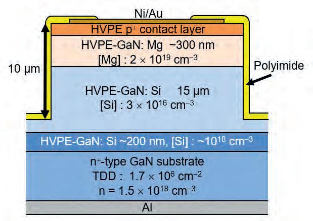
The team from Nagoya produced its devices on a freestanding, HVPE-grown GaN substrate with a threading dislocation density of 1.7 x 106 cm-2 and a carrier
REFERENCE
K. Ohnishi et al. Appl. Phys. Lett 119 152102 (2021) concentration of 1.5 x 1018 cm-3. On this foundation they first deposited, by HVPE, a pair of silicon-doped n-type layers – initially a 200 nm-thick n+ layer, and then a 15 μm-thick n-type layer, grown at 30 μm/hour, with a silicon concentration of 3 x 1016 cm-3. For the p-side they added a 300 nm-thick GaN layer with a magnesium doping concentration of 2 x 1019 cm-3, and a 20 nm-thick GaN contact layer, heavily doped with magnesium.
Crucial to the team’s pioneering of HVPE growth of vertical GaN p-n diodes has been the development of a new approach to magnesium doping. As far back as the 1970s, researchers had realised p-doping in HVPE-grown films using magnesium. However, the high equilibrium vapour pressure of the metal source hampered control of the doping level.
Ohnishi and colleagues have addressed this weakness by switching the magnesium source to MgO, which has a very low equilibrium vapour pressure and a melting point of 2800 °C. The new process involves supplying HCl gas to heated MgO. A reaction results in MgCl2, a precursor for the growth process. One concern with this approach is that MgO could introduce oxygen impurities. However, this does not appear to be an issue, according to Ohnishi: “Fortunately, the oxygen concentration is suppressed, even if magnesium oxide is used. This mechanism is under investigation, but we consider that c-plane growth is effective for oxygen suppression.”
He and his co-workers formed diodes from the epiwafers by: using reactive-ion etching to define 340 μm-diameter mesas that are 10 μm high; activating magnesium acceptors, by annealing samples in nitrogen at 700 °C for 5 minutes; and adding a Ni/ Au anode and an aluminium cathode to the p+ contact layer and the back of the substrate, respectively.
Secondary-ion mass spectrometry revealed a sharp increase in the concentration of magnesium from 5 x 1015 cm-3 in the n-type GaN drift layer to 1.9 x 1019 cm-3 in the p-type layer beside the p-n interface. This indicates that HVPE is capable of producing a steep p+ -n interface.
Current-voltage plots for the device revealed an ideality factor of 1.6, which is lower than that for p-n diodes formed by a combination of MOCVD and HVPE, due to the suppression of silicon at the interface.
Ohnishi and colleagues are now planning to use HVPE to fabricate other vertical devices, such as MOSFETs. “In addition, we are interested in the HEMT.”
Specialists with 30 year+ pedigree and in-depth knowledge in these overlapping sectors:

Expertise: Moderators, Markets, 30 Years + Pedigree Reach: Specialist vertical databases Branding: Message delivery to high level influencers via various in house established magazines, web sites, events and social media
Semiconductor (Silicon/Compound) Publications include: Compound Semiconductor, Silicon Semiconductor, CS China, SiS China
Power Electronics Publications include: Power Electronics World
Future Mobility Publications include: TaaS Technology, TaaS News
Data Centres Publications include: DCS Europe, DCS UK, SNS International
SmartSolar UK & Ireland Publications include: Solar and Power Management, Solar UK and Ireland
Sensors Publications include: Sensor Solutions Magazine, Sensor Solutions International
Digitalisation Publications include: Digitalisation World, Information Security Solutions, Managed Services
Photonics Publications include: PIC Magazine, PIC Conference
Expert Moderators
Dedicated technical and time-served experts/editors
MARK ANDREWS
Mark Andrews is technical editor of Silicon Semiconductor, PIC Magazine, Solar+Power Management, and Power Electronics World. His experience focuses on RF and photonic solutions for infrastructure, mobile device, aerospace, aviation and defence industries
PHIL ALSOP
Journalist and editor in the business to business publishing sector for more than 30 years currently focusing on intelligent automation, DevOps, Big Data and analytics, alongside the IT staples of computing, networks and storage
JACKIE CANNON
Director of Solar/IC Publishing, with over 15 years experience of Solar, Silicon and Power Electronics, Jackie can help moderate your webinar, field questions and make the overal experience very professional
DR RICHARD STEVENSON
Dr Richard Stevenson is a seasoned science and technology journalist with valuable experience in industry and academia. For almost a decade, he has been the editor of Compound Semiconductor magazine, as well as the programme manager for the CS International Conference
For more information contact:
To promote your products and services contact: UK, Europe + Rest of the World USA: Jessica Harrison Janice Jenkins T: +44 (0)2476 718970 T: + 1 724-929-3550 E: jessica.harrison@angelbc.com E: jjenkins@brunmedia.com
Tel: +49 2407 9030 0 Fax: +49 2407 9030 40 Email: info@aixtron.com www.aixtron.com
Tel: +001 610-647-8744 info@appliedenergysystems.com www.appliedenergysystems.com
Tel: +1-408-727-5555 www.appliedmaterials.com

Tel: 1 610-647-8744 purification@appliedenergysystems.com www.armpurification.com
Tel: +1-408-387-5340 Fax: +1-408-809-2883 Email: micro.sales@basf.com www.chemetallprecisionmicrochemical.com Tel: +44 (0)191 332 4700 Fax: +44 (0)191 332 4800 sales.semi@bruker.com www.bruker.com
Tel No: +49 (89) 96 24 00-0 Fax No: +49 (89) 96 24 00-122 Email: sales@csclean.com www.csclean.com

info-gatan@ametek.com www.gatan.com
Tel: +1 408 501 9100 Fax: +1 408 501 9110 Email: sales@innovioncorp.com www.innovioncorp.com
Tel: +1 734-426-7977 Email: requestinfo@k-space.com www.k-space.com
Tel: +44 (0)1244 521869 Email: info@pegasuschemicals.com www.pegasuschemicals.com
Tel: +49 7033 6937-0 info@mbe-components.com www.mbe-components.com

Tel: +1 (603) 883 5200 Email: sicinfo@gtat.com Website: www.gtat.com

Tel: +49 8728 911 093 Fax: +49 8728 911 156 Email: sales@35reclaim.com www.35reclaim.de
Tel: +1 603 595 8900 Email: sales@masimosemi.com www.masimosemiconductor.com
Tel: +1-203-944-2418 Email: michele.pacelli@perkinelmer.com www.perkinelmer.com Tel: + 41 81 403 8000 Fax: + 41 81 403 8001 www.evatecnet.com
Tel: +1 732 494 8660 joanne.lowy@horiba.com www.horiba.com/scientific
Non Contact Measurements Resistance, Resistivity Wafer Thickness
Tel: +49 (0)8122 86676 Fax: +49 (0)8122 86652 Email:info@kitec.de www.kitec.de
Tel: + 1 203 949 8697 Email: info@nelhydrogen.com www.nelhydrogen.com
To advertise here contact: UK, Europe + RoW: Jessica Harrison: T: +44 (0)2476 718970 E: jessica.harrison@angelbc.com USA: Janice Jenkins T: +1 724 929 3550 E: jjenkins@brunmedia.com
Tel: +1 732-735-5655 Email: wma@premissa.net www.premissa.net
Tel: +36 1 505 4690 sales.support@semilab.com https://semilab.com
Tel: +31 24 350 0809 info@trymax-semiconductor.com www.trymax-semiconductor.com
Tel: +1 925 245 5817 Fax: +1 925 449 4096 Email: lwarren@ferrotec.com www.temescal.net
Tel: 516-677-0200-1222 Email: info@veeco.com www.veeco.com
Tel: +49 (0) 3641 79980 Fax: +49 (0) 3641 7998222 www.vistec-semi.com

Tel: +49-89-96090900 Email: ulvac@ulvac.de www.ulvac.eu

Tel: +82 10 8531 2724 overseas@unilok.com http://unilok.com
Tel: +1 949 241 9501 Email: ray@sanan-ic.com www.sanan-ic.com/en
info.epigan@soitec.com www.soitec.com

Tel: + 1 908-403-3304 Email: info@tnsc-innovation.com www.tnsc-innovation.com
Tel: 86-769-2289 3350 Fax: 86-769-2289 3355 Email: enquiry@sicty.com www.sicty.com

Tel: +1 201 507 3300 Fax: +1 201 507 1506 Email: inquiry@umccorp.com www.umccorp.com

Tel: +1-781-933-3570 Email: sales@vacuumbarrier.com www.vacuumbarrier.com
Tel: +4822 733 54 10 Email: info@vigo.com.pl www.vigo.com.pl
Optical Metrology for Wafer Mapping and in Situ Monitoring
Tel: +81(0)88-660-7633 sales@ysystems.jp www.ysystems.jp
Showcase your presence to the global Compound Semiconductor industry for the next 12 months
COMPOUND SEMICONDUCTOR MAGAZINE is the primary information resource for professionals working with compound semiconductor materials and devices.
Each issue of the magazine is distributed in print and digitally to over 60,000 professionals worldwide. With the largest and most diverse global audience of qualified buyers served by any compound semiconductor focused magazine, secure a corporate partnership and buyers guide entry and receive 12 months of promotion and exposure to the compound semiconductor industry across the magazine portfolio including: 12 months of promotion in nine issues of the print and digital versions of
Compound Semiconductor featuring your company logo and company details 12 months of promotion and exposure on the Compound
Semiconductor website
compoundsemiconductor.net
featuring a Buyers Guide entry and hyperlinked company logo Sponsorship of one e-news alerts sent out to over 60,000 industry professionals with text and a standard web banner.
To find out more, contact:
Jessica Harrison Sales Executive E: jessica.harrison@angelbc.com T: +44 (0)2476 718970