
50 minute read
Tim Twining
Indium Corporation has been the only materials supplier known for its focus on reliability on the Automotive Electronics Council. Given its expertise and leadership in this domain, Indium, seems to be tapping the Indian automotive market vigorously. Understanding more about their plans, Niloy of BISinfotech tables an exclusive interview with Tim Twining, Vice President of Sales, Marketing and Technical Support, Indium Corporation. During the interaction, the veteran highlights on their innovative solutions like lead-free solders, Indian market focus, and their strategic leadership in the PCB and SMT Assembly market, and also shares their master plan to keep the tempo during the pandemic. Edited Nub below.
Advertisement
Q. Given 2021, what will be the key offerings and focus of Indium Corporation in India?
In 2021, we’ll continue to focus on the proliferation of electronics in the automotive market. Due to higher power requirements, hybrid and electric vehicles are using electronic power modules at higher and higher voltages and current densities, with long-range-capable battery systems to match. Ensuring long-term reliability drives our innovation in assembly materials for automotive modules and packages.
Indium Corporation’s proven products for automotive applications include: y Indalloy®292, an innovative alloy engineered to provide advanced lifetime reliability to industries requiring highperformance and to address the increased temperatures in many automotive applications.
y Indium8.9HF Solder Paste, an industry-proven solder paste series that delivers no-clean, halogen-free solutions designed to produce low-voiding, enhance electrical reliability, and improve stability during the printing process for high-reliability automotive electronics.
y InFORMS® preforms are innovative reinforced matrix solder composites, which provide even bondline thickness, as well as enhanced joint strength, mitigating reliability challenges for EV modules.
y QuickSinter® silver sintering paste delivers consistent, highspeed sintering on a variety of surfaces and die metallizations. QuickSinter® works well in both high- and low-temperature pressure or pressureless applications. It can be used for discretes, small modules, and integrated power modules.
Indium Corporation remains the only materials supplier on the reliability-focused Automotive Electronics Council.
pandemic including: the medical community for the production of ventilators and pacemakers; fire suppression in producing fire sprinklers; emergency responders, supporting the Vice President of Sales, Marketing development of advanced telecommunication devices; and Technical Support, Indium Corporation and the transportation industry with the production of automotive lighting and aerospace electronics. We meet or exceed best practices for virus containment, minimizing economic hardships on our communities, and protecting our people, their families, and their communities while we continue to supply high-quality materials to the industry. During this pandemic and despite all the challenges, Indium Corporation’s team kept innovating with new materials and processes to meet the demands of new products that are currently or will shortly enter the market. We kept investing in R&D and engineering and installed more manufacturing tools and analytic capabilities than any previous year. To accommodate this increased activity, we increased our manufacturing footprint in virtually all of our facilities and created a new 42,000 sq. ft. headquarters. You will hear about more expansion in 2021.
Q. Your sales and marketing strategies in this new normal?
Like many in the industry, we shifted our marketing and sales focus to digital platforms. For example, we developed and launched our own webinar program—the InSIDER Series—to allow us to continue to share our expert industry insight and products with our customers. We’ve been honored by the success and participation the program has seen so far and will continue to cover exciting topics in 2021 and beyond. For those interested, our archived webinars can be found at www.indium.com/webinar. In addition to our webinar program, we work with industry organizations and media to support them with technical content and advance the industry.
Q. Talking about last year which faced a major turmoil due to the pandemic, Indium Corporation strategies to keep processes and business seamless? Also, segments and regions where your business was mostly hit?
Indium Corporation has continued to support our customers, ensuring essential industries are supplied during the
Q. How are you meeting the advanced needs of the global electronics assembly materials market?
To us, our motto of From One Engineer to Another® is more than
a phrase; it is a commitment to collaborating with customers and partners on the challenges facing our industry. In support of that, Indium Corporation’s team has continued to innovate with new materials and processes to meet the demands of new products that are currently or will shortly enter the market. Throughout the pandemic, this included investing in R&D and engineering. We also installed more manufacturing tools and analytic capabilities than any previous year. To accommodate this increased activity, we increased our manufacturing footprint in virtually all of our facilities, created a new 42,000 sq. ft. headquarters, and added new manufacturing facilities in India (2020) and Malaysia (2021).
Q. What is driving the evolution of lead-free solders? Your offerings and focus into this technology?
When the world was moving toward green manufacturing, lead-free soldering—originally driven by RoHS (Restriction on the use of Hazardous Substances in electrical and electronic equipment) of Europe —was becoming the mainstream for the electronics industry, and Sn-rich alloys—including SnAgCu, SnAg, and SnCu—had been prevailing for more than a decade. While the electronics industry keeps advancing rapidly toward miniaturization, two important drivers are dictating the evolution of lead-free solders: low cost and high-reliability. Indium Corporation has a long legacy in developing lead-free solder solutions designed to meet our customers’ needs. This has included the development of Indium8.9HF Solder Paste, a lead-free product that delivers superior printing and voiding performance, to our ongoing efforts with the Die Attach 5, or DA5, consortium (composed of Infineon Technologies, Bosch, STMicroelectronics, NXP Semiconductors, and Nexperia) to develop high-temperature, lead-free alternatives to traditional lead-containing solders. Indium Corporation’s efforts have led to the development of numerous high-temperature solder products, including BiAgX®, a high-temperature lead-free solder paste, as well as the QuickSinter® silver sintering paste, and Durafuse™ HT, a high-temperature alloy system.
Q. Indium Corporation is a world-leader in solder paste and SMT assembly. How do you find the market out in India? Challenges and scopes.
Indium Corporation works tirelessly through the research and development of our products to prove again and again that materials science changes the world by enabling a large variety of future technologies. These include, but aren’t limited to, novel thermal materials removing heat from highperformance computer chips and ultrafine solder powders of novel alloys, allowing the creation of the tiny solder joints needed for mobile and wearable devices. As a percentage of our sales, India is relatively small today, but the growth rate of both our business and the electronics market in India is tremendous. We are also adding more technical support resources in addition to our new factory in Chennai. We see a bright future for India in the global electronics supply chain going forward and we are proud to be a part of it. We look forward to continuing to participate in local organizations and events.
Q. PCB market in India is quite vibrant and bullish, Indium’s focus into PCB assembly sector and how dynamic it has become with advance technology demand (smaller, sophisticated, and more powerful devices) dominating the market?
Indium Corporation has continued to develop materials designed to meet the evolving challenges of the PCB industry. The demands for smaller, more reliable, and low-temperature solutions create exciting opportunities for the development of innovative enabling technologies. For example, some of Indium Corporation’s newest offerings, such as CW-232, a flux-cored wire for robotic and laser soldering applications, features additional wetting power for higher throughput as well as exceptional post-soldering cleanliness. Where traditional low-temperature solders can product brittle joints, Durafuse™ LT is a low-temperature alloy system designed to provide highreliability in low-temperature applications that need to reflow below 210°C. PicoShot® NC-5M is specifically engineered to support smaller components that require precision materials. Its innovative formulation provides exceptional jetting performance and its unique oxidation barrier promotes complete powder coalescence during reflow to eliminate graping and similar reflow issues.
Q.Any flagship solution you want to highlight for our Indian reader and industry, benefits, pricing, etc.?
We have excellent relationships with our customers as part of our commitment to the collaboration inherent in From One Engineer to Another® and we continue to advance our materials technology. There are almost always trade-offs in solutions, e.g., cost vs. reliability, assembly vs. performance, etc., and we help our customers make those decisions in order to help them achieve the lowest cost of ownership. We have a strong technical team near our customers and a strong development and engineering team at our sites to advance our technology. Almost all of our product development is driven by solving our customers’ challenges.
Q. Lastly, how important is the Indian market for Indium and your future plans for the Indian market?
We are seeing India becoming much more important in the electronics industry due to both domestic demand as well as increasing participation in global supply chains. As a result, we are investing more heavily in the region with local manufacturing and more technical support personnel along with developing local partners. This investment includes the opening of our first manufacturing facility in India, located in Chennai. We are in the process of ramping up production with tremendous support from our customer base in the region. We already have more expansion plans planned for 2021.
Industry Set to Test the Six Nines Capability of New 5G Mobile Technology
Brendan O’Dowd
General Manager, Industrial Automation| ANALOG DEVICES
Until the launch of 5G, every previous generation of mobile phone technology was primarily intended to improve the operation of the handset. First-generation mobile phone networks were analog systems that provided just enough bandwidth for voice calls. Introduced in the early 1990s, 2G was the first digital mobile technology, while 3G in the late 1990s made it possible for handsets to carry email messages and provide rudimentary access to web pages. It was not until the adoption of 4G technology in 2008 that real smartphone capability was enabled: 4G mobile broadband led to the development of smartphone apps, the proliferation of multimedia and streaming services, and access to high speed internet on-the-go.
The recent installation of 5G networks marks the first time that a new generation of mobile technology has been built around the needs of machines and systems rather than handset users. The telecommunications industry’s plan for 5G envisaged technical breakthroughs in three main parameters: ► Latency, reliability, and determinism ► Connection density ► Bandwidth and the speed of data transfer
The reason for enhancing performance in these parameters was to enable real-time monitoring and control of dense concentrations of devices communicating concurrently. In a smart city scenario, for instance, 5G is expected to enable real-time information about the location of available on-street parking spaces to be displayed in the navigation system of cars in the vicinity. Such a smart parking system will require the simultaneous connection of thousands of proximity sensors or cameras and thousands of cars in a small area, continually transferring real-time data about space availability and location. The requirement of this and other applications for latency, density, and bandwidth is met by three technology enhancements embodied in the 5G standard specifications: ► Ultra-reliable low latency communication (URLLC) for real time-control systems ► Enhanced mobile broadband (eMBB) to support new bandwidth-dependent use cases, including augmented and virtual reality ► Enhanced/massive machine type communications (eMTC) for low power, wide area wireless networking These 5G technology features make it capable of supporting the requirements of factory control systems for real-time determinism and six nines (99.9999%) availability. Yet the real-world experience of most mobile handset users accessing 2G, 3G, or 4G networks still involves black spots where coverage is weak or nonexistent, and of occasional and unpredictable dropped connections. So is there a realistic prospect that mobile phone technology will be used to connect mission-critical, time-sensitive industrial machines?
For all the hype around state-of-the-art 5G technology, the reality is that most process equipment installations today include a provision for control via mature wired 4 mA to 20 mA links—a proven, dependable technology that dates back to the 1950s. This speaks to industry’s need for certainty and the avoidance of risk when implementing mission- or safetycritical control systems. But the tides of change cannot be beaten back forever, and innovations in the way factories operate give control system designers good reason to evaluate alternatives to 4 mA to 20 mA technology. As Industry 4.0 and other global phenomena accelerate the pace at which factory operations evolve, two trends are driving the introduction of new networking technologies: the introduction of autonomous mobile machinery and the development of more flexible manufacturing facilities to meet growing consumer demand for personalized or configured products.
In factory and warehouse settings, the use of autonomous guided vehicles (AGVs), cobots, and other types of autonomous mobile devices offer an effective way to increase efficiency and productivity. As automated equipment takes on the burden of performing repetitive and mundane tasks, workers are freed to transfer to higher value and more interesting factory operations that machines cannot perform.

The new generation of autonomous mobile devices such as AGVs requires a wireless communications connection that offers low latency for real-time control, high bandwidth to carry the signals from multiple sensors such as LIDAR scanners and video cameras, and high immunity to interference—the hallmarks of 5G mobile networks.
When factory operators replace wired with wireless connections, they also gain the flexibility to quickly reconfigure factory equipment to meet new or varied demands from consumers. The rise of e-commerce raised expectations from consumers for near-instant delivery of ordered products and for the ability to choose from a wider range of product options than ever before. The ability to move production or process equipment more quickly and easily is growing in value. A fixed, wired communications infrastructure is less flexible than a wireless network to which equipment can connect from any location. Wireless networks also reduce the cost, inconvenience, and technical difficulty involved in installing communications cabling. Over the long-term, then, factory operators are open to the benefits of wireless control capability alongside established wired communications technologies. In the immediate future, however, industry must prioritize its most important requirements, which are: ► High reliability and availability ► Security ► Robustness to cope with challenging industrial operating conditions ► Ultralow latency
These factors underlie the longevity of the 4 mA to 20 mA standard for factory communications. And while factory operators are looking to replace 4 mA to 20 mA technology, their focus today is on the implementation of the time sensitive networking (TSN) standard for wired Industrial Ethernet communications, rather than for anything wireless.
TSN has emerged as the preferred standard for high bandwidth, wired data communications in the factory, since it offers the ideal combination of reliability, robustness, a high data transfer rate, low latency measured in microseconds, and easy integration with enterprise IT network systems. And because the TSN specification is a standard benefiting from cross-industry support, it is rapidly developing a rich ecosystem of suppliers of TSN components and systems, which includes Analog Devices.
OpenRAN: Non-Public Networks Enable the Validation of Claims Made for 5G Performance
Alongside the implementation of TSN networks, the scope for enhancing factory operations through the implementation of wireless networking is also coming under active evaluation. Some early adopters in the industrial community have already begun the work of testing, validating, and evaluating the operation of 5G networking systems inside the factory, while concurrently replacing legacy 4 mA to 20 mA systems with new TSN Ethernet networks. This validation process will find the most suitable applications for 5G technology. So factory operators are now starting to test the innovative features of the 5G specification, such as massive MIMO capability—the use of arrays of antennas to provide multiple physical transmission paths between a transmitter and receiver. An array may be configured to form multi-antenna beams transmitting to multiple receivers. This allows the implementation of techniques such as channel hardening, beamforming, rapid channel estimation, and antenna (spatial) diversity, the effects of which are to dramatically improve reliability and reduce latency compared to 4G mobile networking. Indeed, one of the aims of the developers of the 5G standard was to enable wireless networks to achieve six nines reliability for packet delivery, comparable to that of a wired Ethernet network, and equivalent to a packet error ratio of 1:1,000,000. Latency of just 1 ms is also possible, which is well within the limit imposed by many industrial control applications.
The question is, can this performance be achieved in the real-world conditions experienced inside a factory, where communications equipment might be subject to multiple sources of high amplitude radio frequency interference, transient voltage events, high temperatures, and other disturbances? In validating the real-world performance of a 5G installation, factory system designers have a choice: they can, of course, take advantage of 5G coverage provided by mobile network service providers. But the 5G standard also makes provision for the implementation of private systems, or so-called non-public networks (NPNs) that cover, for example, an industrial campus or a large factory complex. Different industrial users and use cases will favor a different choice of public or private network. The implementation of 5G networking in the factory is also facilitated by developments from mobile network operators of the OpenRAN (Open Radio Access Network) specification. This has opened the market for 5G radio and core equipment to a broader range of suppliers in addition to those which traditionally served the telecoms equipment market. This has the potential to broaden the choice of equipment available to meet the needs of use cases different from those of massmarket public network operators and to encourage the development of 5G products by suppliers that are focused on the industrial market.
As a supplier of physical layer components and protocol software to manufacturers both of TSN equipment and of 5G infrastructure, Analog Devices is ideally placed to assess the prospects of each technology for implementation in industrial control systems. While the immediate future belongs to wired Industrial Ethernet technology, it is easy to imagine a future where AGVs and robots inside the factory transmit and receive time- and mission-critical data payloads via a 5G network—and the availability of 5G network coverage means that this is an actual rather than a theoretical possibility today.
About the Author
Brendan O’Dowd has over 30 years of experience in the industry working for companies like Tellabs, Apple, and Analog Devices. He is currently the general manager of Analog Devices’ industrial automation business. He can be reached at brendan.odowd@analog.com.

KevinKing
Senior Manager, Electrical Design Engineering Company:-Renesas Electronics Corporation
My Smart Lighting System is Telling Me it is Unsafe in this Room!
We are all waiting a return to social and business normalcy after the Covid-19 vaccine is successful. Whether in a conference room, meeting room, cafeteria, or break room, all will start being used again enabling groups of people to gather to interact face-to-face. Prior to Covid-19, how many of you remember the meeting coordinator saying, "we’ve been here awhile, let's take a short break" or "I am feeling like I need a breath of fresh air"? Even working from home, how often have you found yourself taking frequent breaks to stroll around the house because you feel a bit "worn" from sitting in a closed home office?
Build-up of carbon dioxide (CO2) and volatiles expelled by human breath in these tightly closed rooms generate, in part, "unhealthy" air quality. If we could detect the decline in a room’s air quality and "warn" people or automatically turn the ventilation up, this would be a great solution. All these rooms have one thing in common, lighting. Many of today’s new lighting systems are "connected" for ease of control for color, presence and ambient light detection.
Connected lighting is expected to grow in all geographies, even expanding to older building retrofits. Since lighting modules are so pervasive, it would be logical to add a simple sensor
module so they could monitor the lighting and "unhealthy" levels of gases such as CO2. Designers of a lighting system would just need to add a few extra bits of data to the already existing communications infrastructure.
Renesas’ connected lighting solution, including air quality and lighting, shows a typical connected lighting block diagram (Figure 1). The sensor array contains an HS3001 for temperature and humidity, a ZMOD4410 for indoor air quality (eCO2 and TVOC gas monitoring), and an ISL29125 for monitoring ambient light and color control. We also have a ZMOD4510 outdoor air quality sensor for entry ways, streetlights, loading docks, etc. In addition, connectors are provided for optional PM2.5 sensors.
Image
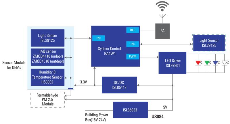
Figure 1. US084 Connected Lighting with Air Quality Solution
The US084 Sensor Module (Figure 2) is available and uses the standard mikroBUS™ click format, allowing it to be used or evaluated with any MCU development kit providing a "Click" socket.
Image
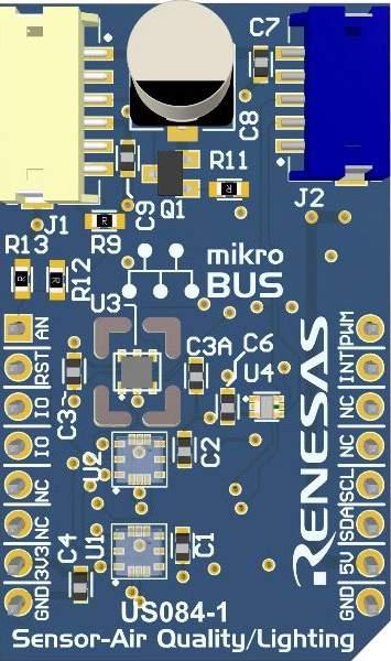
Figure 2. US084-1 Sensor Module
The next evolution in environmental air quality is here. So, when your LED lighting system tells you to "get some fresh air", do not be surprised.
Sports Innovated:
The Influence of Motor Racing on Next Generation Passenger Vehicle Development
With total annual viewing figures measured in the billions, motor racing represents one of the world’s most popular televised sports. It gains widespread media attention and generates huge sponsorship revenues. With many of the world’s leading automotive brands participating in some form of motorsport, it provides a valuable platform for these companies to showcase the strength of their engineering credentials. As well as being of value competitively, car manufacturers appreciate the other plus points that motorsport involvement brings in terms of contributing to their ongoing product development programs. Many of the technological wonders that were first seen on the racetrack have eventually been adopted into passenger cars - resulting in enhancements in performance, improvements in fuel economy and higher degrees of occupant safety. Key innovations that stem from this source relate to hybrid engines, in-vehicle networking, the acquisition of diagnostic data, more effective camshaft arrangements, automatic transmission systems, improvements in aerodynamics, use of advanced chassis materials and regenerative braking.
A New Era of Motorsport Endeavor
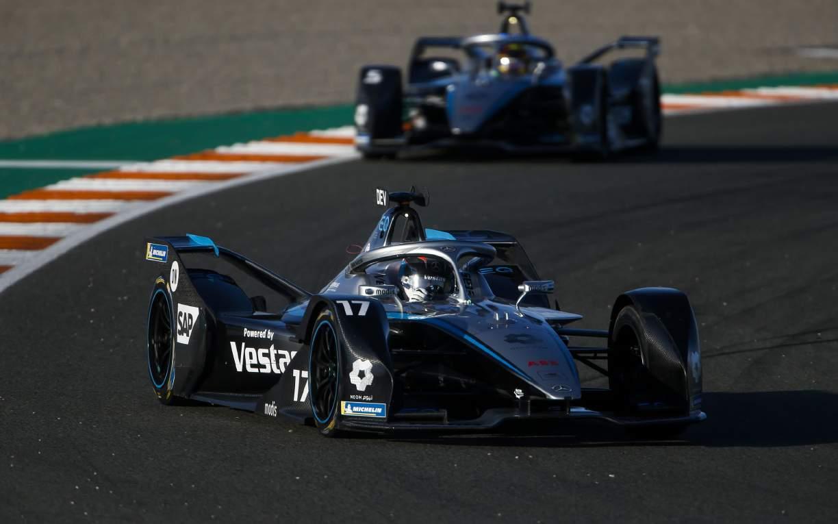
With the prevalence of electric vehicles (EVs) now starting to grow significantly, the ABB FIA Formula E World Championship race schedule is now being recognized as vital testbed for automotive ingenuity. With a very engaged and continuously rising global fan base, its E-Prix events are helping to dispel the myth that EVs can’t be exciting. There are an array of high-profile automotive brands taking part in this competition, including MercedesEQ®. There is, once again, huge potential for technology to crossover into mainstream cars - particularly in relation to energy recovery mechanisms or power management systems.
In Formula E, the format is constantly evolving - with teams needing to be able to respond accordingly. For example, the first four Formula E seasons, drivers had to change cars halfway through the race, ditching the one they had originally started with for a second fully charged car. In Formula E’s fifth season (in late 2018), this all changed. From that point onward, the cars of all competing teams needed to have the battery capacity to complete that whole race, without any substitutions. To address this change, the teams’ technical staff have had to make huge steps forward in the operational efficiencies of their vehicles, as well as boosting energy storage densities substantially.
Dave Priscak
VP, Worldwide Solutions Engineering, ON Semiconductor
Bringing Formula E Engineering into Real World Scenarios
So let’s now look at the ways in which what is happening on the racetrack will have an effect on the EVs that we will be buying in the years ahead. There are several areas where the technology developed for Formula E Generation 2 race car should have long term benefits to mass market EV designs. Here are some of the most important ones:
1. The battery technology - a key obstacle that needs to be overcome if the commercial uptake of EVs is to be accelerated is allaying consumers' worries about not being able to travel adequate distances in such vehicles before they run out of charge. Through experimentation with new battery chemistries, combined with improvements to powertrain efficiencies (both of which have been derived from work being done in Formula E race car to some extent), EV models now on the market are capable of covering over 200 miles before needing to be recharged. At the same time, comprehensive roll-out of charging infrastructure and the advent of fast charging technology are each helping to address consumers ‘range anxiety’ issues still further, by ensuring charging can be done in a quick and convenient manner.
2. The powertrain - for the powertrains in both Formula E race cars and mass market EV models the objectives are much the same. These are predominantly to maximize power transfer efficiencies as much as possible (by employing sophisticated motor algorithms, undertaking switching at faster speeds to avoid losses) and supplement battery reserves via use of kinetic energy recovery mechanisms. By successfully achieving these objectives, the rate at which the battery depletes will be slowed and the range that the vehicle can cover before needing a recharge will be expanded.
The main power bus used in the majority of consumer EVs will currently have a 400 V (voltage) rating. Through the impetus provided by Formula E race cars, where higher voltage powertrains are already utilized, 800 V systems are now being developed for mass market deployment. These elevated voltage figures will not be addressable using conventional silicon power discretes. They will instead call for the incorporation of wide bandgap devices, such as those based on silicon carbide (SiC) process technology. SiC already features in the powertrains of Formula E race cars, with its elevated levels of efficiency and resilience to harsh operational conditions proving to be extremely advantageous. ON Semiconductor is playing an integral role in Formula E powertrain development. For example, it has assisted the Mercedes-EQ Formula E Team in developing ultra-efficient powertrain systems through use of superior automotive-grade power devices. The two companies have worked closely together on improving the efficiency levels at the traction inverter power stage. What has been learnt from projects like this is then subsequently being leveraged to improve consumer EV powertrain efficiencies.
3. Fast charging - migration to higher voltages is already underway within the EV mains bus - helping to increase operational efficiencies and combat potential wastage. It will, however, also be of considerable value from a charging perspective, allowing transmission losses to be curbed. Much as prospective EV customers have concerns about vehicle range, they are also keen to ensure that charging doesn’t present unwanted difficulties. The charging technology for the latest generation of Formula E race cars enables 4kWh worth of charge to be supplied in an interval of just 30 seconds. Such speeds won’t be achievable by consumer charging points for a very long time yet (with electrical distribution grids struggling to support this, as well as there being issues in relation to the current carrying capabilities of the charger and cabling). Nevertheless, the period taken to fully charge EVs is constantly being shortened - and this trend will continue, with incorporation of the latest wide bandgap power semiconductor devices being of paramount importance here.
4. Regenerative braking mechanisms - regenerative braking is an important aspect of Formula E race cars, as it means there are greater available energy resources that the race car can access. In a racing scenario, where hard braking is commonplace, there is clearly ample opportunity for regeneration. That said, the time taken to capture this energy during a hard brake is not long enough for it to be transferred back into the battery. Supercapacitors provide a means of temporarily storing the recovered energy, so that it can then be returned to the battery, or applied back to the motor when the race car starts to accelerate again. Inclusion of these supercapacitors is justifiable in Formula E designs, but their high price tag will preclude them from use in consumer EVs, where costs need to be kept in check. Also the brake to run ratio will be far lower in consumer EVs, and so the benefits derived will not be as great. Even so, EV manufacturers are putting a lot of engineering effort into the development of cost-effective energy recovery systems for mass market deployment.
Conclusion
The relationship between innovation in motorsport and the development of better road vehicles is still very much apparent. Formula E race cars like the Mercedes-EQ Silver Arrow 02 are now taking on the mantle as a technology drive Formula E is the global platform for OEMs designing new EV models and specifying the constituent components. The ongoing knowledge transfer that arises from it will be pivotal in enabling society’s vehicle electrification goals to be met.
ON Semiconductor has been heavily involved in this knowledge transfer. The company is able to draw on the experiences it has gained at Formula E racetracks and research centers, plus the expertise it possesses in SiC and gallium nitride (GaN) technology, then apply this to EVs on our roads. In doing so DC/DC conversion can be made more efficient, plus higher voltages and faster switching speeds can be attained. Through such innovations, EVs will become a much more attractive option to the car buying public, and over time this will help to increase the proliferation of these vehicles.
Indium Software to Develop More IPs and QA Space
Indium Software, a well-known name in technology solutions companies with deep expertise in Digital and QA services has been serving a wide range of customers from several industries including Banking, Technology, Healthcare, Life sciences, Retail and Education. Indium Software’s Digital Solutions focus on offering Data Engineering Services, Advanced Analytics, Application Development (Full Stack & Mobile) and Low-Code Development services to its clients. While talking with Nitisha from BISinfotech, Srikanth Manoharan, SVP, QA solutions, Indium Software shares his plans on investing in R&D to develop more IPs in the Digital and QA space.
Q. Kindly share the growth journey of Indium Software from QA to Digital Services to Product IP.
Indium has been a forerunner in the QA space for almost 2 decades, we have been a “quality custodian” for many customers, and we continue to do so. We stay ahead of competition through constant innovation in our services and offerings. As the industry began to take new avatars like Digitization, Digitalization and recently Digital transformation, Indium launched solutions to aid in this transformational journey. One of the strong success factors is our product IPs, both on the QA and Digital front, which attract many customers as it gives bespoke and ready-to-deploy solutions. IPs - uphoriX - Smart Test Platform and teX.ai – Text Analytics Product.
Q. What is the role of QA in digital transformation? How QA contributes/ benefits the digital transformation objectives?
Be it IT or Manufacturing, QA always gets paramount importance in any field, though it is termed differently e.g. QA, QC etc. In the digital world, we are making systems smarter, intelligent, powerful and resilient. This has led to transformation in development methodology too e.g. Waterfall to Agile, Monolithic architecture to Microservices architecture, Bare metal to Cloud, DevOps, DevSecOps and the list goes on. In digital development, there has been a huge absorption of open source into development, developers have zillions of reusable codes and frameworks available, the quality of such open source are not guaranteed unless we put them in proper testing. We are also seeing the advent of “Low Code” platforms like “Mendix & Claris” to build applications. These applications pose challenges of a different kind. This makes QA an indispensable part of digital transformation.


Srikanth Manoharan
SVP|QA solutions|Indium Software
Q. How was the year 2020 in terms of business and what will be your marketing strategy for the upcoming year?
December 2020 was possibly the best one we have had. Indium signed on nearly 30 new customers between April and September, a 11% increase from a 2019. A significant portion of this was in Q2, post July 2020.
The ongoing pandemic has hamstrung most of us. Sales Leaders and Marketing Leaders across industries are immobile. NO -
events, meet-ups, in-person meetings, travels, luncheons, etc. There are many interesting things on the digital marketing front that we focus on to help increase traffic and generate more inbound demand.
• Keyword Optimization - We optimize on-page and off-page SEO. Ranking for long-tail keywords, which tend to have high conversion rates, is vital in the quest for maximum inbound traffic. • Content Repurpose - To complement SEO efforts and generate traffic, we create content on a large-scale, repurpose it for multiple channels. • Reference Platforms – Then, there’s branding content, which is vital to enhancing a brand’s online and offline image. • Digital Adaption – We have been utilizing this time to analyze historic data from Google Analytics, CRM, SM handles, and other sources to initiate new marketing campaigns We regularly update our marketing collateral and other resources, optimize UI/UX and ensure the right message is conveyed to the target customers.
Q. Kindly share Indium's Business vision for India and global market.
We clearly see that IP based solutions deliver tremendous value to our customers. We will invest heavily in R&D to develop more IPs in the Digital and QA space.
Our presence is predominantly in the US Market and India. We plan to diversify and increase our business in UK, Europe and APAC in the coming years.
We, as an organization have learned to set the bar high in terms of benchmarks. From a revenue standpoint, we plan to grow at 40% CAGR for the next 2-3 years given the tailwinds the technology industry is seeing.
Q. Kindly explain the digital transformation testing journey.
In terms of QA , the way organizations should stay abreast with the dynamic nature of the digital transformation journey by adopting a transformation in the Quality space as follows: • Quality Assurance (QA): These are our traditional testing methods which still are relevant in some cases. • Quality Engineering (QE): Testing the code as white box, early in the development stage using Automation along with Devops. • Intelligent Quality (IQ): Measurement driven assessment using code instrumentation, AI based prediction on failures to become proactive rather than reactive.
Q. During the lockdown and given the pandemic situation how Indium Software performed?
We have been fortunate that a large segment of our customers did well in 2020. There was an air of caution and “wait & watch” mode during the April to June 2020 period. Post that and as the Work from Remote and New Normal’s settled in, we have seen a resumption to pre-Covid levels of business activity and IT projects by our clients. There are few cases impacted negatively but by and large we have not seen any major disruption to our business, which helped us grow over 30% in 2020.
Q. Latest announcement for the year 2021?
We are targeting to do $30 million in revenue by 2021. As mentioned previously, we will invest heavily in R&D to develop more IPs in the Digital and QA space. We plan to diversify and increase our business in UK, Europe and APAC. From a revenue standpoint, we plan to grow at 40% CAGR for the next 2-3 years given the tailwinds the technology industry is seeing.

Five Ways to Protect Augmented Reality Wearables from Electrostatic Discharge Damage

Design for connectivity, reliability, and safety using the latest
circuit protection technologies and board layout strategies Todd Phillips Global Market Manager, Electronic Business Unit, Littelfuse, Inc.
Those of us who wear vision correction glasses are used to seeing the world through lenses. New technologies now allow a virtual world to be layered on top of the real world that we normally see. The lenses will become displays that allow us to see the “real” world that is augmented with overlaid information and images, creating an Augmented Reality (AR). An example would be the integration of navigation into the AR glasses to allow a user to walk through town with turn-byturn instructions (visual or verbal) to help them easily get to their destination. Other examples include facial recognition, fitness tracking/health-sensing, travel assistance, business news, first-person photos and videos (Figure 1).

Figure 1. Example statistical information visible using Augmented Reality (AR) glasses.
This article discusses advanced circuit protection solutions and board layout strategies that safeguard wearable devices and their users. Applying these recommendations early in the design process will help today’s circuit designers improve the performance, safety, and reliability of their wearable technology designs and help build a more reliable IoT ecosystem.
ESD Selection and Configuration Factors for TVS Diodes utilized in AR wearables
1. Increasingly Smaller Form Factors
Today’s ESD diodes offer a variety of performance benefits for AR applications led by a small form factor (Figure 2). To optimize their future circuit designs, design engineers should follow these recommendations for the selection and configuration of ESD diode technologies.

Figure 2. Available IC areas, form factors, and circuit protection components continue to shrink in size as the sophisticated chipsets used in wearable devices get increasingly smaller.
Figure 3. The SP3522 Series lowcapacitance bidirectional discrete TVS diode arrays provide symmetrical ESD protection for high-speed data lines when AC signals are present. They are also designed for consumer electronics such as smartwatches, smartphones, tablets, eReaders, and fitness bands.

2. Choosing unidirectional or bidirectional ESD diodes
ESD diodes are available in both unidirectional or bidirectional configurations. Unidirectional diodes are used for DC circuits, including keypads, pushbuttons, and digital circuits. Bidirectional
diodes are used in AC circuits, which may include any signal with a negative component greater than -0.7V. These circuits include analog video, audio, RF interfaces, and legacy data ports.
Where possible, electronics engineers should choose unidirectional diode configurations to improve performance during negative-voltage ESD strikes. During these strikes, the clamping voltage is based on the forward bias of the diode, which is usually less than 1.0V. During a negative strike that is based on the reverse breakdown voltage, a bidirectional diode configuration provides a clamping voltage that is higher than the forward bias of a unidirectional diode. Thus, the unidirectional configuration dramatically reduces the system stress experienced during negative transients.

Figure 4. The SP1020 from Littelfuse provides robust ESD protection in a very space efficient 01005 package making it ideal for applications like AR Glasses where board space is very limited.
3. Determine diode location
Board-level ESD diodes at each of the IC’s pins are not required in most circuits. Instead, the circuit’s designer should determine which pins might be exposed to user-generated ESD events that occur outside of the application. If the communications or control line can be touched by the user, it becomes a possible pathway for ESD to enter the integrated circuit. Typical circuits include buttons, switches, USB, audio, and other data buses. While incrementally adding these discrete devices, it is important to reduce the size to fit 0201 or 01005 outlines to avoid using too much board space. There are also space-saving multi-channel arrays available for many wearable applications. Place the ESD device as close to the ESD ingress point as possible, which is typically defined as the connector or the I/O.
4. Consider routing of “ESD” trace
To protect the IC’s pins with an ESD diode, there are several key considerations for trace routing—from I/O to ground. ESD, unlike lightning transients, does not unleash a large amount of current for a long duration of time. It is important to move the charge from the protected circuit to the ESD reference as quickly as possible to effectively handle ESD. The length of the trace are the overriding factors—from the I/O line to the ESD component and from the ESD component to ground— not the width of the trace to ground. Trace lengths should be kept as short as possible to limit parasitic inductance. This inductance results in inductive overshoot, which is a brief voltage spike that can reach hundreds of volts if the stub trace is too short. Recent package developments, include µDFN and Wafer Level Chip Scale Packages (WLCSP) utilize outlines that fit directly over the data lanes to completely eliminate the need for stub traces.
5. Understand HBM, Machine Model (MM) and Charged Device Model (CDM) definitions
HBM, MM, and CDM are test models for characterizing the ESD robustness of the integrated circuits that run the portable device or wearable, including the processor, memory, and ASIC. They are used by the semiconductor supplier to ensure the robustness of the circuits during manufacturing. The current trend is for suppliers to reduce the voltage test levels since it saves die space. Additionally, most electronics manufacturers not only provide for ESD protection, they have countermeasures in place during the assembly process.
If ESD protection is only becomes a consideration during assembly, then once the device reaches the consumer, the device is susceptible to ESD damage in the consumer’s environment. Without adequate ESD countermeasures built in, electronic devices will fail incrementally or catastrophically in the user’s environment. To guarantee fewer ESD related field failures and thus happy customers, electronics design engineers should select a board-level device that is robust enough to protect against intense electrical stresses yet offers the bandwidth and the electrical performance demanded by the end-user product. When evaluating ESD protection components, consider the following parameters:
• Dynamic resistance: Defines the diode’s resistance to the change in state from blocker to conduit of electronic energy. This value represents how quickly the diode will clamp and divert the ESD transient pulse to ground. It helps define how efficiently the avalanche diode conducts the excess voltage and current to ground. The more vertical the I-V or TLP curve is, the more efficient the avalanche diode is, and the lower the expressed dynamic resistance. • IEC 61000-4-2 rating: Tested and confirmed during design and characterization, this rating reflects what the ESD diode is capable of withstanding repeatedly without degradation of the DC performance. Typically for this parameter, the higher the value, the better. A growing number of Littelfuse ESD diodes approach 20kV and 30kV under contact discharge conditions, which regularly exceeds industry standards for fielded electronics, nominally 8kV air discharge. • DC (Direct Current) Performance: When designing circuits that need protection, remember these important considerations: • Parasitic capacitance, • Parasitic inductance, • Surge tolerance (8/20us), and • Nominal and maximum leakage currents.
The approach will vary depending upon the performance characteristics of the interfaces being protected.
For additional information on ESD protection for wearable devices, download the ESD Suppression Design Guide and Wearables Protection Application Note, courtesy of Littelfuse, Inc.
This article was written by Todd Phillips, Global Market Manager, Electronic Business Unit, Littelfuse Inc., Chicago, IL.
2K Conformal Coatings Address Performance Challenges in the Harshest Environments
Phil Kinner
Electrolube Technical Director (Coatings Division)
Introduction
The performance requirements of coating materials continue to become ever more challenging, as electronics are subjected to ever more hostile operating environments, including higher temperatures along with increased levels of salt-spray and condensation. As OEMs try to save weight from their designs, the use of robust metal assembly housings are being replaced by less hardy designs, transferring increased performance requirements to the assembly, such as continued operation under full immersion conditions. Simultaneously, environmental legislation continues to evolve, with an emphasis on reducing solvent usage and VOC emissions. In response to these ever increasing performance challenges, a new generation of two-part 2K conformal coatings have been developed by Electrolube to provide even greater protection, compatible with the protection offered by an encapsulation resin, however, with the easy application of a coating. The 2K series of coatings have been rigorously tested in comparison to UV and silicone coatings in a variety of harsh tests, which have included thermal shock, powered salt-spray, condensation and mixed flowing gas (MFG) testing, which will be explored further in this article.
Firstly, let’s examine the driving forces for using conformal coatings in harsh environments. Given that the conformal coating is often providing secondary protection (housing normally provides the main barrier properties), it is useful to consider the main threats that must be mitigated against and other unique demands caused by the long service lifetimes of the assemblies, when selecting a suitable conformal coating material for harsh environments. The vast majority of decisions to use coatings traditionally falls into one of the following 4 categories:
1. Protection against corrosion in end operating environment (Humidity, Corrosive gases, Salt-spray etc) 2. Protection against condensation in end operating environment 3. Reduction in component spacing to meet safety or design criteria 4. Tin whisker mitigation
By considering the requirements of each application independently, some common themes emerge.
Corrosion is a complicated, diffusion controlled, electrochemical process that takes place on an exposed metal surface. Despite the vast variety of potential mechanisms and causes, in the majority of cases, there are 3 requirements that must be fulfilled in order for corrosion to take place. 1. Intrinsically electrochemically dissimilar metals (e.g. Gold/ Silver and Nickel/Tin), or the creation of an anode and cathode by application of applied bias. 2. The presence of an ionic species (usually Salts, Halides, Hydroxides etc). 3. The presence of mono-layers of condensed water to dissolve the ionic species, resulting in an electrolyte solution.
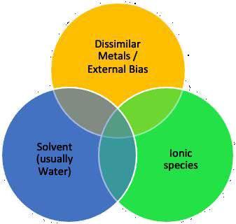
In order to prevent the possibility of corrosion, it is necessary to remove one of the pre-requisite conditions. The choice of metals is limited to those used in the solder and solder finish chemistries (which are dissimilar), and there will always be areas of potential difference due to the nature of an electronic assembly. Cleaning can help remove ionic species, but cannot prevent the re-deposition of ionic species from the operating environment.
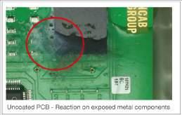
Conformal Coatings help prevent the formation of electrolytic solutions by acting as moisture barriers. Given the 3D topography of metal surfaces on a PCB, all metal surfaces need to be sufficiently well coated to prevent exposure of the metals surface to a potentially corrosive environment, in order to provide the maximum degree of protection. Small voids in the coating that expose the metal surface can actually accelerate corrosion under the right environment. The conformal coating challenge is achieving the required level of coverage on the three-dimensional, complex topography of exposed metals. In addition to perfect coverage, the coating also needs to be a good barrier against moisture and provide good adhesion to the substrate to prevent delamination. Once the coating is delaminated, moisture can eventually collect in this ‘pocket’ and form an electrolytic solution with any preexisting ionic contamination. This is the reason that cleaning prior to conformal coating is recommended, to provide a powerful synergistic elimination of two of the three pre-requisite conditions for corrosion.
2 Protect against condensation
Whenever there is a significant level of humidity, there is always the opportunity for parts of the assembly to drop beneath the dew point, resulting in the formation of condensed water on the surface of the assembly, which can significantly reduce the insulation resistance of the boards surface, resulting in the malfunction of electronics.
Whilst pure water is not a great conductor of electricity, any ionic impurities (e.g. salts from manufacturing or end use environment) will become solubilised and will form a conductive pathway, leading to corrosion as described above. Higher levels of liquid water can rapidly accelerate this process.
In addition to corrosion, condensation severely tests the insulation resistance of the coating. Considering this is essentially an immersion application, water will very quickly find weak spots or voids in the coating. Whether there is no coating, or the coating is thin, the insulation provided will be negligible or less than optimal. The conductive solution can carry the current from one weak spot to another very quickly, resulting in either immediate failure, which may be reversible when the board dries out again, or which may be permanent if conductive corrosion products, dendrites (metallic filaments) or other permanent sources of current flow are deposited on the surface of the coating.
3 Reduce component spacing
Although air is normally an excellent insulator, it can begin to break down when stressed by a sufficiently high voltage (an electric field strength greater than about 3 kV/mm), becoming partially conductive. Across gaps, breakdown voltage in air is a function of separation. If the voltage is sufficiently high, complete electrical breakdown of the air will culminate in an electrical spark or an electric arc that bridges the entire gap. Conformal coatings provide additional insulation resistance and can be used to enable designers to make their designs more compact, by placing components closer together than would otherwise be possible.
4 Tin whisker mitigation
The application of conformal coating is a tin whisker mitigation strategy. Conformal coatings mitigate the risk of tin whiskers generating a short in one of three ways. a) A tin whisker eruption needs to puncture and penetrate out through the coating. Research shows that this is unlikely. b) In order to short, the protruding tin whisker must either: a. meet another protruding tin whisker from an alternative polarity b. penetrate back through the coating at a place of opposite polarity to create a short.
All of these situations for forming a tin-whisker short are unlikely (but not impossible) events. Research and modelling show that as long as you have adequate coverage and thickness of conformal coating on conductive surfaces leads, it is unlikely for tin whiskers to penetrate through the coating once, and almost impossible to do so twice. That leaves the only real potential failure mechanism as two protruding tin whiskers meeting and forming a short, which is a statistically insignificant probability.
By considering these 4 case scenarios, it should be clear that the coverage of the applied conformal coating must be as close to perfect as possible. In addition, it should be recognised that the greater the thickness of conformal coating achieved, the greater the protection will be from the environment.

For conventional liquid-applied materials and application processes, achieving good coverage and thickness has been shown to be problematic in the IPC’s ‘state of the industry assessment’, with literally thousands of cross-sections analysed, showing zero (for all practical considerations) coverage on many common component leads and bodies for all material/ process combinations.

Manual Spray applied UV curable material Selectively applied UV curable material
Cross-sections courtesy of Rockwell-Collins.
Given the importance of edge-coverage and thickness and the challenge in achieving both, while still maintaining other performance requirements (e.g. temperature resistance,
thermal shock resistance, cycle-time etc.) a new coating concept was developed to reliably meet these increased performance demands.
The Two-Component (2K) Approach
Electrolube developed the 2K conformal coatings series by way of providing a solution to common problems faced by manufacturers with performance issues of current coatings in harsh environments. The 2K series of coatings is significantly different in its protective capabilities due to its capacity for greater coating thickness and enhanced edge coverage. 2K coatings are VOC-free, fast-curing, high performance two-part conformal coatings that provide a solvent-free alternative to both UV and silicone materials, require less capital investment than UV materials and improve on the performance of most silicones in harsh environments. The majority of coatings in the 2K range are hydrophobic, giving excellent protection against water immersion, salt mist and humidity, making them ideally suited for automotive electronics.
2K materials are commonly used in high performance industrial applications such as adhesives, paints and even potting materials. The systems consist of a resin portion and a crosslinker portion, that are reasonably stable when kept separate. However, once mixed in the correct ratio, an unstoppable chemical reaction begins which continues until a solid polymer is formed. By adjusting the nature of the resins and the hardeners, a wide variety of polymers can be produced from soft-rubber like materials to high-strength glass-like materials. Many of these materials are diluted with solvents, which increases the usable life of the system and enables the use of existing application methodologies. However, with the restrictions on solvent-usage, it was decided to focus on generating a solvent-free solution.
Moving to a solvent-free 2K system required the development of a special applicator to facilitate this technology as shown below.
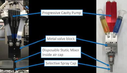
Images courtesy Nordson Asymtek and Precision Valve and Automation (PVA)
The approach uses twin progressive cavity pumps to control the metering of the two reactive components, keeping the materials separate until the mixing process, which occurs in a small, disposable static-mixer, immediately prior to application. Utilising this approach of mixing immediately prior to application, enables the use of more reactive materials, resulting in shorter cure times. The atomised spray application enables a wide range of material viscosities to be selectively applied within a normal cycle time. The use of larger pumps can enable faster cycle times, and the all metal design of the applicator provides the opportunity to heat the material to improve process consistency and enable the use of more viscous materials.
This applicator technology enables all of the 2K range of materials to cure within 10 minutes at 80°C, the typical drytime and temperature for a solvent-based acrylic. Indeed, the latest addition to the 2K range cures primarily with UV radiation (conventional microwave or arc-lamp systems (UVA) or the latest LED curing technology), whilst the chemical cure ensures complete-curing within shadowed areas in just a few hours, compared with weeks or months for moisture initiated secondary cure mechanisms.
Coverage and thickness
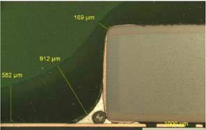
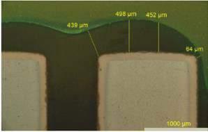
The following cross-sections demonstrate the achievable thickness and coverage for a variety of common components.
It should be clear from the following sections that the 2K materials enable a much greater thickness and perfect application coverage, to provide a higher level of protection. Performance advantages of the 2K materials can be demonstrated in three of the harshest tests employed by users today.
Thermal Shock
Coated automotive ECU assemblies subjected to 1000 thermal shock cycles from -40°C to +140°C without stress cracking.



Powered Condensation Testing
A populated Electrolube SIR test board was used to evaluate the NPL’s new condensation test method, prior to the launch of the current ongoing project.
The boards were tested uncoated, selectively coated with a solvent-based acrylic and selectively coated with a 2K material.
The board and test results for a BGA device and an SOIC are shown below. The results show that for both component types, the SIR results with the 2K coating remained 2 orders of magnitude higher and did not vary much whether the material was covered with condensed water or not. However, for the acrylic there was a fairly significant difference depending on whether the material was under condensing conditions or not. The BGA device showed evidence of dendrite formation in the uncoated evaluation.
Powered Immersion testing in salt-water


In order to assess the ability of the coating material to withstand powered immersion in salt-water conditions, two experiments were performed.
Firstly, standard IPC B-24 SIR coupons were spray-coated and cured at a variety of different thicknesses, achievable from a production process. The SIR coupons were placed in a horizontal position and powered up at 10V. Each SIR pattern was covered with 5% (w/w) saline solution, and the patterns were monitored to ensure they remained completely saturated with saline throughout the test duration. SIR measurements were recorded every minute. The experimental set-up is shown in Fig A.
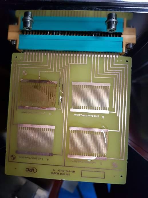
Fig A. SIR experimental set-up
The SIR measurements for the OSP coated Cu, Reflowed SAC alloy, Ultra-thin conformal coating (3 micron) and Acrylic conformal coating (50 micron) are shown below in Fig B. Whilst the acrylic material showed very low SIR values, the results were at least consistent and significantly better than the Cu-OSP value. Interestingly, the SAC alloy showed reasonable resistance to Saline, whereas the UT coating was indistinguishable from the OSP coated CU, both of which showed evidence of electrochemical corrosion.

Fig B. SIR comparison of Acrylic, Solder Paste, UT and AR coatings
However, when we look at the results for the 2K materials during this same test we can see that within the intended thickness range (>100 micron), there is no impact from the salt-immersion throughout the duration of the 30 hour test. At 50 micron thickness, the SIR shows some impact of the saline immersion, but the results are still 3 orders of magnitude greater than the UT or AR materials.
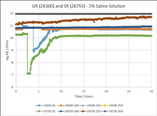
In the second immersion study, IPC-B52 test coupons were coated with 2K300, 2K850, UT and AR type materials by a normal application process. The coupons were cured in accordance with supplier recommendations and left or 28 days prior to commencement of the immersion test.
Conclusion

The 2K range of materials provide sharp edge coverage and protective thickness, unrivalled by other liquid applied conformal coatings. The materials have been developed specifically for thick film applications and engineered to optimise this performance advantage, whilst mitigating many of the issues associated with thick coatings, such as cracking during thermal shock testing and solder-joint lifetime degradation, especially for very sensitive devices such as BGA packages. The rigorously tested two part systems can be applied thinly (50-75μm), however, they have been designed, formulated and tested to be applied at much greater thicknesses (150300μm), to facilitate superior encapsulation of components and component leads.
The materials will drop into any existing selective coating process with a simple valve modification and minimal investment. The extreme protection provided by the increased thickness and superior coverage will be valued by many Automotive and Aerospace suppliers struggling with increased demands from OEMs for improved condensation resistance and even powered up sea-water immersion conditions.
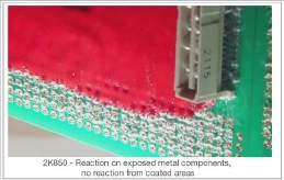
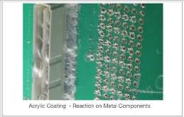
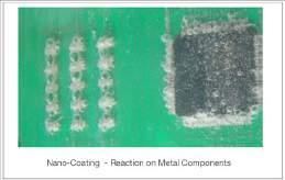
The boards were immersed in saline solution and then immediately powered at 5V. The boards were filmed during their immersion. A significant degree of bubbling and the formation of corrosion products could be seen almost immediately with both the uncoated control and the UT coating material, especially on the components. The Acrylic coated board showed almost immediate bubbling, but the formation of corrosion products took approximately 2-3 minutes.
The 2K300 and 2K850 boards showed no evidence of bubble formation throughout the 30 hour duration of the immersion test.


