
33 minute read
Eric Wong
The Power Behind Vicor Packaging
Q: How would you characterize the evolution of Vicor within the power electronics domain, and what was the driving force of this evolution?
Advertisement
Vicor has been on the forefront of power delivery network (PDN) performance for decades by continually innovating on four essential technology pillars, spanning power delivery architectures, control systems, topologies and packaging.

Each pillar has multiple layers and all are essential to advancing the performance of Vicor power modules. However, the innovations in power system architecture, control systems and topologies would have little impact apart from the central pillar of packaging. Without innovating power module packaging technology, the industry-leading advances in power density, current density and efficiency could never be realized. Power module packaging is a unique differentiator for Vicor and has been a core competency since the company’s inception. From its first Brick product to today’s ChiP™, Vicor has been continually innovating its packaging technology to deliver better solutions for power systems engineers.
Q: What was the genesis of the Vicor product portfolio in terms of power packaging?

Figure 1 — Vicor Maxi, Mini and Micro DC-DC Bricks revolutionized power systems design in the 80's with a new high-power-density module package consisting of an overmolded board assembly mounted onto a baseplate for heat extraction.
Eric Wong
Vice President|Sales Asia Pacific|Vicor
Every innovation begins with a spark of an idea, of how technology can improve performance to better meet customer challenges. Sometimes innovations are ahead of the curve, and it takes time before early adopters comprehend the full potential of the innovation. This is what happened with the Vicor modular power component concept that brought the DC-DC converter module to market as a building block for designing advanced power system solutions in the 80s. Vicor modules were way ahead of the competition in terms of density and efficiency and they were packaged in a format that resembled a brick—hence the name Bricks. The Brick consisted of an overmolded circuit board assembly mounted onto a baseplate for optimal thermal management. This was a highly differentiated approach to power conversion, and Vicor Bricks drew interest from early adopters in the emerging communications, defense and industrial markets. Power system engineers realized that a decentralized, modular approach to their power system design would allow them to handle the increasing number of loads in their system and that Bricks had many advantages over bulky, centralized, multi-output power supplies. In fact, the advent of the Brick was key to the development and acceptance of distributed power architecture at the time.
This new power module provided a flexible, scalable solution which was essential for advanced power systems design. Vicor continued to drive the evolution of the Brick package by being the first to market with the Half-Brick and then in the 90s the first to offer the Quarter-Brick.
Q: How did Vicor power packaging progress from the original Brick package format, and what were the benefits?

Figure 2 – VI Chip® packaging was necessary to fully realize the breakthrough advances of the new FPA™ (Factorized Power Architecture) and advances in topologies and control systems
In 2008 Vicor introduced three new innovations. 1. A new architecture called FPA™ (Factorized Power Architecture) 2. A new topology called SAC™ (Sine Amplitude Converter) 3. ZVS and ZCS (zero-voltage and zero-current switching) control systems
Collectively they reduced power losses dramatically and drove a new package development, the VI Chip, initially in a one-inch-square package with a height just over a quarter of an inch, which could take full advantage of the improved efficiency and power density the three innovations.
The VI Chip packages were further developed as half, full and double sizes and were manufactured in individual cavities where their PCBs were fully overmolded with a thermally effcient molding compound. The VI Chip package had surface-mount J-lead pins or straight pins for though-hole mounting.

Figure 4 The new panel manufacturing process was another innovation for the power industry. ChiPs are all cut from the same panel size enabling a manufacturing operation that is very scalable.
Q: How did manufacturing scalability factor into the next generation of Vicor power products subsequent to the VI Chip packaging?
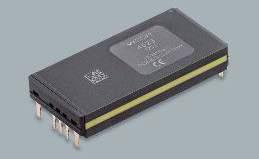
Figure 3 – The new ChiP package was distinguished by its two-sided component assembly while being cut from fixed-size panels, similar to how silicon chips are made and cut from wafers.
In 2015 with further improvements in control systems, topologies, components and materials, the VI Chip® package was redesigned to capitalize on further power-loss reductions, higher-frequency control systems and topologies with resulting gains in power and current density. The new package was called the ChiP™ (Converter housed in Package), and although it looked similar to a VI Chip, its construction and manufacture was very different.
Instead of an individual cavity construction as in the VI Chip package, ChiPs are made and cut from a standard-size panel and full utilization is made of both sides of the module’s PCB for active and passive components. Thermal management of this package must take this into account with a double-sided cooling design to maximize performance and power density. Making and cutting ChiPs from panels is very similar to how silicon chips are made and cut from wafers, but whatever the power level, current level or voltage level of the module, ChiPs are all cut from the same panel size enabling a manufacturing operation that is very scalable. This advancement in package design and manufacturing offered significant advantages in terms of increased power and current density, plus highvolume automation and cost reduction.
Q: To what extent did mounting configurability and thermal management considerations impact the evolution of the ChiP packaging platform?
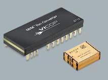
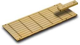
Figure 5 – Following completion of the molding process, the panel of surface-mount CM-ChiPs is copper plated to provide terminal connections for power and signal pins.
ChiP packaging technology came under scrutiny again when Vicor advanced its innovations in control systems and topologies with a fourth generation (Gen 4) of power conversion and regulation ASIC controllers. The Gen 4 controllers enabled further advances in efficiency and power and current density. To take full advantage of the Gen 4 control silicon improvements in converter and regulator performance, the decision was made to retain the basic panel construction but with one difference: after completion of the molding process, the panel would be copper plated to provide terminal connections for power and signal pins.
Figure 6 – The newest CM-ChiP packaging enables chassis mount, surface mount and pin-mount options
The plating also enables thermally adept high-power front end AC or DC converter modules utilizing advanced cooling schemes. The new fourth-generation ChiPs advance performance significantly (see Figure 6) and keep Vicor on a track of consistently cutting power losses by 25% every 2.5 years.

Figure 6 Advances in power and current density enabled by cutting power losses by 25% every 2.5 years and advancing power module packaging technologies
Q: What are the core target applications for Vicor ChiPpackaged power products, and what are the key design challenges?
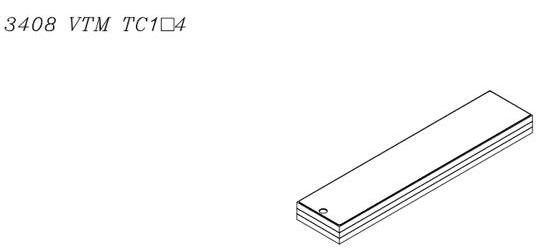
More recent innovations in ChiP packaging are enabling several new high-growth applications. One of the most demanding is advanced artificial intelligence (AI), where processor current levels have risen above 1000 amps. In these applications, power distribution losses in board and substrate copper power planes has become a dominant loss term and performance limiter. These applications require extremely high-current-density power modules that can be mounted as close as possible to the processor power pins to reduce these losses. Additionally, transient performance (di/ dt) can also be affected by the impedance between the power module and the processor. This is a critical term when processor workloads are suddenly increased and immediate current draw is needed.

Figure 7 Vertical power delivery to advanced AI processors with stacked ChiPs reduces board and substrate power losses to improve processor performance
To meet the requirements of these demanding applications, and minimize impedances it is necessary to deliver power vertically by positioning the power modules directly under the process and exactly matching the power modules’ output power pins with the power pin array of the processor. Typically, this would result in a board layout conflict because this is also the optimal location for the large number of bypass capacitors required for energy storage to meet instantaneous processor power demands.
Q: How can this ‘vertical power delivery’ architecture benefit from Vicor ChiP technology?
The challenge of vertical power delivery (VPD) has been met with a ChiP stacking technology. The new VPD power modules consist of a current multiplier layer and a “gearbox” layer which holds the bypass capacitors and changes the pitch of the current multiplier to match the pitch and layout of the AI processor power pin map above. This new ChiPstacking technology enables AI processor power system designers to deliver power in the most optimal way and to get the maximum performance out of their processor for high-performance computing (HPC) applications.
Q: How would you summarize the overall Vicor philosophy on power packaging?
The four pillars of Vicor innovation are completely intertwined, and each pillar has many elements and layers to it. Enabling the highest performing modular power delivery solutions and continually advancing power and current density demands that power module packaging is developed ahead of the delivery of control system, topology and architectural innovation advances. The Vicor ChiP packaging approach focuses on the miniaturization of every single component and element that makes up the module. As Vicor makes further improvements in performance, ChiP packaging will take on new levels of innovation, the journey is nowhere near over.
Anritsu New RF Regulatory Test System

Anritsu Corporation has released its new RF Regulatory Test System ME7803NR solution for regulatory compliance testing of 5G communications systems.
The newly developed RF Regulatory Test System ME7803NR uses the Radio Communication Test Station MT8000A as a simulated 5G NR base station in combination with a spectrum analyzer and signal generator to implement ARIB/ETSI/FCCcompliant FR1 RF tests.
Key Features:
• Supports World Regional Frequency Bands Certified North-American, European, and Asian bands, as well as other future regional bands to be deployed (5G NR Bands and 5G NSA mode LTE Bands for LTE Anchor), are supported.
• Maximizes Value of Customers’ Prior Equipment Investment Customers can configure the ME7803NR test system by adding their own Anritsu standalone test equipment, such as the MT8000A, MT8821C, MS2840A/MS2850A, MG3710E, MG3694C, etc., to minimize additional required hardware purchases.
Keysight’s New AresONE-S Test System
Keysight Technologies has introduced new AresONE-S 400GE test system which enables network equipment manufacturers and data center operators to validate complex, mixed 400 gigabit Ethernet (GE) and lower-speed networks and devices.

Data center operators have widely deployed mature 100GE non-return-to-zero (NRZ)-based technologies. However, higher Ethernet speeds, such as 400GE, create new mixed signaling and forward error correction (FEC) implementations in data center networks, as well as multi-rate speed environments.
Keysight's AresONE-S test system also provides:
• An ultra-high-density, 2 rack unit (RU) fixed chassis to deliver optimal rack space footprint. • The IxNetwork software application, a Layer 2 and 3 protocol emulation platform that runs end-to-end tests with an extensive list of networking protocols and data plane traffic to test network infrastructure performance.

R&S at MWC Shanghai 2021 Yokogawa to Offer OpreX Batch
Rohde & Schwarz Solution Soon has demonstrated its market-leading solutions Yokogawa Electric for mobile devices, Corporation reported that chipsets, infrastructure they began providing and networks live at OpreX Batch Solution on the Shanghai New March 17. International Expo Center (SNIEC). This solution for batch Roll-out of 5G in full swing manufacturing applications eliminates the overlap between process control system (PCS) Rohde & Schwarz is demonstrating highlights from its portfolio and manufacturing execution system (MES) related work and of test solutions for 5G base stations and end-user devices. helps to enhance efficiency through all phases of the plant For base station testing, Rohde & Schwarz offers its high-end lifecycle, from design and engineering to actual operation, instruments, the R&S SMW200A signal generator and the R&S modification, and expansion. For use as a central element FSW signal and spectrum analyzer. Also, Rohde & Schwarz of OpreX Batch Solution, Yokogawa has also developed showcases their R&S 5G NR signaling test solution for FR1 Integrated Recipe Manager (IRM), and did release this and FR2 frequency bands based on the R&S CMX500 radio product on the same date. communication tester.

Rohde & Schwarz provides the industry with standardcompliant test and measurement solutions to ensure regulatory compliance and the correct operation of wireless systems within vehicles. At MWC Shanghai, Rohde & Schwarz demonstrates protocol conformance test systems for C-V2X standards, and an advanced C-V2X hardware-in-the-loop test solution to verify telematic control units (TCU) in complex road traffic scenarios. In addition to needing to rapidly develop and deliver new products, batch manufacturers face the challenge of maintaining stable operations while dealing with shortages in the availability of experienced personnel. To address these issues, Yokogawa is offering OpreX Batch Solution, an integrated portfolio for batch manufacturing processes that are aligned with both the ISA-88 Batch Control standard and the ISA-95 Enterprise-Control System Integration standard.
For Automotive ADAS/Infotainment application,
CISPR25 Class5 compliant 8 rails power tree Reference Design with power rail monitoring for supporting functional safety
Introduction
In recent years, the importance of advanced driver-assistance systems (ADAS) that support a high level of Automotive Safety Integrity Level (ASIL) has increased as automobile accident prevention measures and autonomous driving progress. Automated driving requires a vehicle's on-board control system to replace the human driver in performing the four elements of human driving: “Cognition” with the ears and eyes, “Prediction” and “Judgment” with the brain, and “Operation” via the steering wheel and accelerator. For safe automated driving, accurate sensing, timely control and fast display imaging are necessary. For the unit to achieve safety requirements, it is also necessary to monitor the internal operating conditions and take care of any lack of functionality because of unit failure. In order to achieve this, the number of installed cameras and sensors to monitor any external situation are increasing and multi-functionality to inform and display these situations are required in the infotainment system. With the addition of electronic circuits to monitor the operating conditions in each unit, the electronic circuits are becoming more complex and a greater amount of time is being devoted to the design of units and systems.
The market requirements for Reference Design
With increasing the number of on-board units and the number of required functions, the electronic circuits of ADAS/ Infotainment peripheral units require more complex designs. 1) An optimal combination of cost, size and characteristics are necessary as the number of cameras, sensor units and mounted electronic components increase which result in more complex power supply rails. To adapt these market requirements, ROHM has developed a reference design that satisfies the design elements required for unit design, and has disclosed the available design data on website.
Overview of Reference Design (REFRPT001)
An overview of developed reference design (REFRPT001) as follows: 1) Cover the necessary power systems for ADAS and Infotainment applications with an eightcircuit power tree.
2) Built-in Primary(*1) DC/DC Converter ICs (BD9P series) for stable power supply even immediately after battery cranking.
3) Built-in Secondary(*1) DC/DC Converter ICs (BD9S series) with an industry-leading small and highly efficient.
4) Built-in Power Supply monitoring IC with self-diagnostic functions that monitors the all eight output rails to contribute to improve functional safety level.
5) The following items were validated in the system level. - Standard Electrical Characteristics test - EMC test (CISPR25 Class 5 compliant without input filter) - Thermal performance test (separate located high-efficiency DC/DC converters distribute the heat)
6) On-board ICs and discrete parts are automotive AEC-Q100 or AEC-Q101 grade compliant.
7) Main ICs are functional safety products in the FS supportive(*2) category.
A reference board (REFRPT001-EVK-001) outline of the reference design (REFRPT001) (Figure 1) and a system block diagram (Figure 2) are shown below. It is designed to supply power to SoC, MCU, and CAN devices from two primary DC/DC Converter ICs (BD9P series) by splitting into four outputs each. It can also monitor the power rails of all eight outputs, helping to improve the level of functional safety systems.
2) A highly efficient power supply system is necessary since traveling distance cannot be sacrificed.
3) It is difficult to see the problems in a single product consideration since there are different noise standards (e.g., CISPR25 Class 5) that have to complied with for automotive units and many design elements other than functional design that have to be catered for.
4) In order to improve the safety function as a unit or system, it is necessary to have a function to monitor the power rail, detect the failure of the electronic circuit, and transmit it to the CPU.

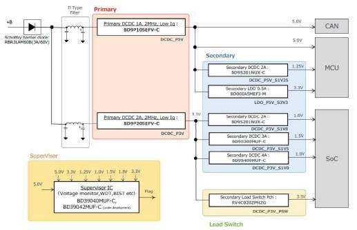
Figure 2. Reference Design (REFRPT001) Block Diagram
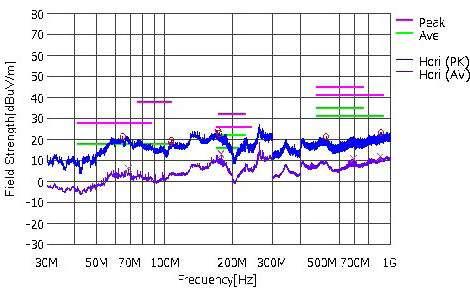
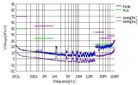
The following are EMC test results disclosed as evaluation data. It is shown that EMC radiation noise (vertical antenna) (Figure 3), radiation noise (horizontal antenna) (Figure 4), and conduction noise (Figure 5) passed CISPR25 Class 5, even with the entire board in operation without input filter. Since an input filter, which improves noise margins is also implemented in the pattern, it is possible to take additional measures for EMC problems that would take a lot of man-hours to fix if they occurred in a unit.
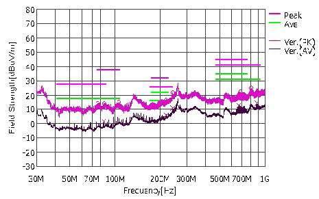
Figure 3. Radiation Noise (vertical antenna) Figure 5. Conduction Noise
Content and tools to fully support customer’s design
The design data of this reference design (REFRPT001) is available on ROHM website. In addition, various design support tools are available. - Reference Block Diagram, Reference Circuit, BOM - PCB information / PCB data - Test report (Standard Electrical Characteristic, EMC, Thermal) - Part of design can be simulated with free web simulation tool (ROHM Solution Simulator) - Spice Model of mounted products - Symbol and Footprint of mounted products - Thermal simulation model of mounted products
As mentioned above, the part of this reference design can be simulated using ROHM Solution Simulator(*3). The ROHM Solution Simulator is a free web-based simulation tool, and reference circuits including peripheral circuits are available. It allows users to perform simulations easily without preparing any simulation circuits or models.
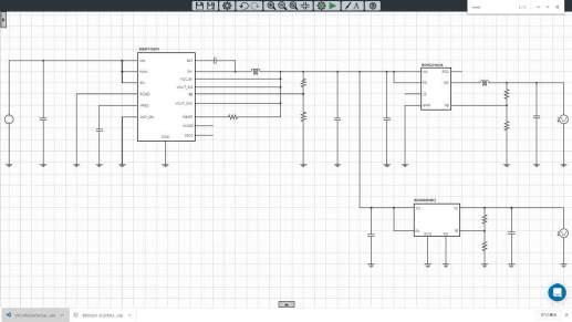
An example of simulation is introduced below: - Simulation of a two rails power tree with a secondary DC/ DC converter (BD9S201) and LDO (BD00IA5M) behind the primary DC/DC converter (BD9P105) connected battery input. (Figure 6) **Simulation circuit is here. My ROHM registration is required.
BD9S201 5.5V 2A DC/DC
BD9P105 40V 1A DC/DC
BD00IA5M 500mA LDO
Figure 6. two rails power tree simulation circuit (1)
- Simulation of a three rails power tree with a secondary DC/ DC converter behind the primary DC/DC converter (BD9P205) connected battery input. (Figure 7) **Simulation circuit is here. My ROHM registration is required.
BD9S201 5.5V 2A DC/DC
Table 2. Line up of Secondary DC/DC Converter BD9S series

BD9P205 40V 2A DC/DC BD9S300 5.5V 3A DC/DC

BD9S400 5.5V 4A DC/DC
Figure 7. three rails power tree simulation circuit (2)
Utilizing these reference design data and simulator in the design of ADAS/Infotainment units can greatly reduce the number of unit design cycles by eliminating the process to select components and ensure to validate the circuit specification.
Advanced technology products that support distinctive reference designs The distinctive reference design is made up of products with advanced technology and features.
y BD9P Series (with Nano Pulse Control™(*4) technology) - 42V Automotive Primary DC/DC Converter Series. (Table 1) - Quick response to provide a stable power supply for battery cranking. - Low EMI noise with a switching frequency spread spectrum function. - FS supportive category of functional safety products.
Table 1. Line up of Primary DC/DC Converter BD9P series
y BD9S Series - Automotive Secondary DC/DC Converter Series. (Table 2) - Contributes to high reliability of the system with Output voltage monitoring function and soft-start time variable function. - 2mm x 2mm small package and industry-leading high efficiency. - 2.2 MHz (typ.) switching frequency without interference to the AM band. - FS supportive category of functional safety products. y BD39040MUF-C - Power Supply monitoring IC with built-in self-diagnostic function (BIST) to support functional safety. (Figure 8) - Built-in Variable watchdog timer (window type), over voltage monitor, under voltage monitor and reset functions. - Built-in self-diagnostic function (BIST) as well as system power rail monitoring to detect potential failures. - Redundant internal reference voltage circuits and oscillator circuits to significantly reduce the probability of failure. - FS supportive category of functional safety products. - Small 3mm x 3mm package make it easy to add to the system.


Figure 8. Feature of Power Supply Monitoring IC BD39040MUF-C
y RBR3LAM60BTF This is a high-reliability, automotive grade (AEC-Q101 compliant) 60V Schottky barrier diode. In this reference design, it is used as a battery input backflow prevention diode. To minimize the dropping voltage due to the diode's forward voltage (Vf), the RBR series has been used with low Vf.
y RV4C020ZPHZG A highly reliable, 1.5 V drive, low ON-resistance, automotive grade (AEC-Q101 compliant) Pch MOSFET. It is packaged in a bottom electrode package for high mounting reliability, and the wettable flank shape does not impair visibility after mounted. In this reference design, it is used as a load switch to split the 3.3V system.
Conclusion
ROHM will continue to develop advanced products and reference designs to apply them to applications, thereby save energy, downsizing, reducing heat generations, reducing design man-hours and improving functional safety level for customer’s units. We believe that our sustaining and continuing efforts will bring safety and security to the automobile society and bring rich lives to people all over the world.
[Terminology]
(*1) Primary, Secondary In a multi-rail power system, the first stage conversion circuit from the battery or other power source is called the Primary. The second stage conversion circuit connected to the output of the primary is called the Secondary.
(*2) FS supportive ROHM categorizes the forms that can be provided for functional safety by product. The component-level forms are necessary to achieve functional safety in the unit. For detail information: https://www.rohm.com/functional-safety
(*3) ROHM Solution Simulator This is a free simulation tool that runs on the official ROHM website. Solution circuits, which is close to application circuits such as circuits combining SiC power devices with gate driver ICs, can be simulated. It reduces design and circuit verification man-hours. For detail information: https://www.rohm.com/ solution-simulator (*4) Nano Pulse Control™ This is one of the Nano series, an innovative power supply technology developed by ROHM. The ultra-fast pulse control technology enables a significant improvement in the conversion ratio and fast response time in power supply ICs. It helps to reduce BOM costs in the system. For detail information: https:// www.rohm.com/support/nano
*Nano Pulse Control™ is trademark or registered trademark of ROHM Co., Ltd.
[References]
ROHM official web site. “New Ultra-Compact Automotive Grade Buck DC/DC Converters” https://www.rohm.com/news-detail?news title=ultra-compact-automotive-grade-buck-dc-dcconverters&defaultGroupId=false
ROHM official web site. “New Power Supply Monitoring IC with Built-In Self-Diagnostic Function that Supports Functional Safety” https://www.rohm.com/news-detail?news-title=power supply-monitoring-ic-with-built-in-self-diagnosticfunction&defaultGroupId=false
(The article is an original piece written by ROHM Semiconductor.)
ROHM Develops Wi-SUN FAN Module Solution
ROHM has established a new Wi-SUN FAN, Field Area Network module for infrastructure applications, capable of connecting up to 1,000 nodes in a mesh network. Wi-SUN FAN the latest Wi-SUN international wireless communication standard, which eliminates the communication costs associated with conventional LPWA (Low-Power Wide-Area) wireless standards.
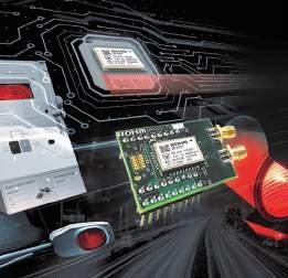
In response to these challenges, ROHM developed the BP35C5, an in-house ultra-small (15.0mm × 19.0mm size) Wi-SUN FAN module. This solution can connect with up to 1,000 devices (e.g., traffic signals and streetlights), enabling the configuration of a remote wireless management system covering an entire city. The BP35C5 also includes the necessary security functions for carrying out secure communication without the need for complicated control. Certifications acquired under the FCC (Federal Communications Commission) and ARIB (Association of Radio Industries and Business) allow for immediate use both in the US and Japan. Other countries and regions will be supported shortly.
The BP35C5 module and BP35C5-T01 evaluation board will be available for purchase in mid-February 2021 through online distributors Digi-Key and Mouser. Various documents and user guides are now available on ROHM’s website. Wi-SUN FAN (Wireless Smart Utility Network for Field Area Network profile) is the latest protocol under the Wi-SUN international communication standard with over 95 million units shipped worldwide.
Whereas conventional LPWA standards support only startype networks, Wi-SUN FAN enables the configuration of mesh networks capable of performing multi-hop transmission between relays, while allowing for remote management of terminal-mounted applications via bidirectional communication between relays and terminals. This makes it possible to automatically optimize the hop route between relays in the event of communication failure due to newly constructed buildings or other surrounding obstacles
Unlike other LPWA standards that incur communication costs for each terminal, Wi-SUN FAN can be operated at little to no cost.
PCB Autopsy – Pre and Post Coating Variables That Cause Board Failure Phil Kinner Electrolube’s Global Business & Technical Director for Conformal Coatings

Conformal coatings are widely used in high reliability and safety critical applications, where the impact of electronic failure can have very serious consequences including loss of life. To ensure a conformal coating meets the desired requirements, coated assemblies need to be exposed to a range of environments via appropriate test conditions to establish the performance range and limitations. Basic tests include electrical performance and accelerated humidity testing, whereas advanced testing can imitate severe conditions such as salt mist, temperature extremes or rapid environmental changes. Conformal coatings are designed to protect PCBs and ensure that they work efficiently in their end-use environment. However, there are instances where boards may not perform adequately or may even fail entirely despite being coated, which in turn produces an expensive, time-consuming nightmare that also impacts on your reputation. Phil Kinner, Electrolube’s Global Business & Technical Director for Conformal Coatings, explores why testing is so important and examines different variables that can cause board failure.
As electronics evolve to do more in an ever smaller footprint, the chance of failures increase more and more. As components get smaller and pitches become ever finer, many designs are getting closer and closer to design rule limits and sometimes even challenging the limits of manufacturability. It stands to reason, that the more designers push the boundaries, the chance of failure increases dramatically. In addition to design related failure issues, the closer proximity of components due to the higher density inherently makes the hardware more vulnerable to corrosion, which is a complicated, diffusion controlled, electro-chemical process that takes place on an exposed metal surface, in the presence of water and ionic contaminants. Cleaning prior to conformal coating will go a long way to removing conditions for corrosion, enabling a more efficient coating process to increase the insulation resistance in these sensitive designs and mitigate against the effects of the operating environment on failure.
As PCBs are highly complex, there are so many variables that can potentially cause board failure. Some failure mechanisms occur slowly, which can help with detection, maintenance and even repair, however, with a sudden and unanticipated failure mechanism, complete PCB failure is often more likely. When a PCB fails despite being coated first, the chances are that there were problematic conditions already prevailing on the PCB prior to the conformal coating process, further still, the coating itself could have been inappropriate or the coating method deployed was not suitable for the application. Equally, there are many other threats to a PCB’s success, which include applying conformal coating to components and surfaces that have not been cleaned prior to coating, electro static discharge or even potentially poor construction of the unit itself.

The first and most critical procedure to employ is to carry out an inspection prior to coating. This is essential because it validates the overall quality of the PCB, ensuring it is fit for purpose and in keeping with customer specifications. Inspection at this stage is also paramount in detecting any conditions that could potentially cause board failure such as component failure, insufficient board thickness and loose connections that impact on connectivity. Conformal coatings do have their limitations and contaminants present on the surface prior to coating will be sealed in by the operation and may cause long term problems – such contaminants might include fingerprints, flux residues and moisture as well as other atmospheric pollutants. Boards should always be cleaned and dried before conformal coating to obtain optimum performance. Even when using so-called no-clean fluxes, cleaning boards before coating helps to increase performance and reliability.
Another renowned enemy of PCBs and components is heat. During operation, the materials within the PCB will undergo a wide range of temperature changes and each component has a specified range of heat that it can absorb, largely dependent on its size and shape. Higher power, greater density electronics produce more heat and excessive heat can cause significant mechanical stress that can impact on solder connections and burn out components. It is essential to manage heat transfer efficiently to increase the lifetime of the device and prevent failure. Overheating not only accelerates failure mechanisms but can also cause devices to become too hot to handle and, in some cases, present a fire risk.
In addition to the issues surrounding heat, the continuing drive towards miniaturi¬sation means that we don’t have space for multiple boards, and there is an increase in the number of designs utilising mixed technologies where analog, digital, and RF circuits are closely combined with high voltage cir¬cuits, it becomes increasingly difficult to satisfy both clearance and creepage design requirements. Even very slight changes in the environment, whether it is an increase in dust, higher humidity, water-splash or exposure to potentially corrosive gaseous materials can be enough to take an otherwise safe, functional design outside of safe operating clearance and creepage, and cause performance failures.
Other contributing factors to board and component failure include poor solder joints, unconsumed or superfluous flux and tin whiskers. Cold solder joints, which occur when the solder fails to melt entirely during assembly, produce poor surfacemount connections that burn components and create power problems. Left over flux can also contribute to corrosion, due to its absorption of moisture, and produce short circuits and damage to components. Tin whiskers also cause short circuits. Conformal coatings can normally combat the formation of tin whiskers during operation, but are less effective when whiskers exist already within the assembly prior to coating. In general, the level of mitigation provided depends more on coating coverage than the properties of the coating, although there is some equivocal data that harder and tougher coatings provide more mitigation, but this must be balanced with an increased impact on the life of the solder joint. Overall, focussing on achieving 100% coverage of metal surfaces is likely to be a more efficient mitigation strategy.
Trace damage can occur from power surges, lightning strikes and overheating. Damage to the silver or copper conductive pathways can normally be seen with the naked eye, but this is not always the case. Trace damage causes considerable issues with conductivity, components and the reliability of the device. Fortunately, trace damage is normally detected and remedied during the initial inspection as it is visually very apparent.
Whilst this is not an exhaustive list of every single factor that contributes to PCB failure, it should help to provide a comprehensive overview of key elements to look out for. Lastly, the design itself could be responsible for PCB failure.

To increase the lifetime of the board, it is imperative to ensure that the appropriate components and materials have been selected, the board layout is sufficient and the design is verified for its specific requirements. Design is also important in determining the appropriate coating application methodology and therefore the cycle times and the costs involved. Some simple things, like trying to keep connectors or other no-coat areas on the same edge of the assembly, can make a huge difference to the ease of coating an assembly, the cost of coating that assembly and, of course, the overall reliability of the assembly.
PCB malfunction post coating
There are a number of variables that could be responsible for a malfunctioning printed circuit board following the coating process. Generally, the results could indicate poor product selection and/or application, or some underlying problem arising from insufficient surface preparation or some chemical activity going on beneath the coating that is entirely unrelated to the coating chemistry. Poorly performing coatings risk loss of insulation at the PCB surfaces when water condenses in combination with ionic impurities to form conductive pathways between PCB tracks. Without doubt, condensation can severely test the insulation resistance of a coating. There are many coating products that resist these sorts of conditions, so this type of problem can be avoided by making an appropriate material selection at the outset.

If the coating has not cured properly, it will not be able to develop its protective properties to the full. In this incidence, the application process is to blame. Correct application is a pre-requisite to coating success and by achieving this, a whole raft of problems can also be solved in one hit. For instance, poor coverage, insufficient thickness and sharp edge coverage can be difficult to achieve with many coatings and it can be hard to ensure sufficient thickness in these areas to maintain protection. A combination of material selection and application technique/workmanship will remedy these sorts of issues. The IPC specification allows a dry film thickness of between 30 and 130 microns, the greater thickness being achieved by the application of multiple coating layers. Trying to achieve a 130 micron dry film thickness from a single selective-coating process with a solvent-based acrylic material, for instance, is a recipe for a disaster, likely to result in excessive bubble formation, film shrinkage, coating de-lamination and additional stress on components. The result is poorer protection, rather than an improved overall level of circuit protection. Aiming for a uniform 30-50 microns and focusing on achieving perfect coverage at each application is a much better approach to improving the protection of electronic circuits.

Achieving the correct coating thickness is important; bear in mind that if the coating is too thick it can lead to entrapment of solvents in areas where the coating does not fully cure. Similarly, it can cause the coating to crack as it cures, or even cause cracking of the coated components themselves, or as the result of changes in temperature, or due to mechanical shock and vibration. The number one determinant of success for coating reliability lies in the application. Often a poor material applied well can be just as good or sometimes better than a material with great properties that is applied badly. Coating is about getting sufficient coverage of the sharp edges and metal surfaces without applying the material too thickly elsewhere. Of course, some materials ‘apply better’ than others and make this process as easy and foolproof as possible; but in the end, the performance of liquid applied coatings will always be determined by how well they were applied.
Large arrays of discrete components also represent a massive coating challenge due to the high levels of capillary forces present and the result is often quite disastrous, with areas of no coverage/protection on the board and conversely areas of excessive thickness prone to stress-cracking, delamination and other coating defects. Ultimately this will lead to premature failure of the assemblies and should be avoided if at all possible!
There may also be an unexpected interaction with some other process material used to prepare/build the PCB. Flux residues are particularly illustrative of this type of problem. In a ‘no-clean’ process, for example, these can inhibit the cure of some types of coating or lead to a loss of insulation of the system, greater than either material in isolation. Unless there has been meticulous attention to preparation or precoat cleaning regimes, corrosive residues bridging the PCB’s conducting tracks can, over time, cause failures. And while the coating may delay failure for many years, at some point failure will inevitably happen. The greatest test of conformal coating’s performance is posed during power-up under wet conditions, whether this is due to condensation, immersion or salt-spray. Water with soluble impurities is electrically conductive and, finding any weak spots in a coating, will eventually leading to short-circuits at the PCB surface. In order to provide protection in these circumstances, it is essential to achieve 100% defect-free coverage of the PCB’s metal surfaces, and this poses a real challenge for both the material itself and the application process. Fortunately, a new class of two-part conformal coating materials dubbed ‘2K’ enable a much greater thickness and perfect application coverage to be achieved, resulting in a far higher level of protection. The superior performance advantages of Electrolube’s 2K coating materials, which combine the tough, resistant properties of an encapsulation resin with the easy application of a coating, have been positively demonstrated in three of the harshest tests that these materials can be subjected to, including powered condensation testing and powered immersion testing in salt-water.
Conclusion
PCBs are the life force of all electronic devices that we rely on every day, from smart phones, tablets, PCs and laptops to street lighting, TVs, refrigerators, microwaves and cars. When a PCB fails it can be enormously disruptive and in cases such as aerospace applications, it can be critical. Therefore, the materials selected to protect electronic assemblies can literally make or break a printed circuit board, particularly if it is required to endure substantial physical shock and thermal cycles. Pre and post coating inspections and tests are essential to ensure that the PCB will perform reliably and increase its lifetime, particularly if the PCB is destined to operate in a harsh environment. Select the appropriate material for the protection required, apply and cure it well. Check for interactions with other process chemistries and thoroughly clean the assembly prior to coating. If possible, spend time simplifying the coating process at the design stage. By the simple action of placing as many connectors and components that must not be coated, as possible along one edge of the assembly, the conformal coating application process will be simplified. PCB failures can unfortunately occur following the application of a conformal coating but the positive news is that failure can be prevented with systematic pre-coat inspections, correct material selection/application method and further rigorous post-coating tests.


