8 minute read
Industry and Research News


Escape From Flatland: Calibration Method Enables Microscopes to Make Measurements in 3 Dimensions
June 24, 2021, NIST News — Conventional microscopes provide essential information about samples in two dimensions—the plane of the microscope slide. But flat is not all that. In many instances, information about the object in the third dimension—the axis perpendicular to the microscope slide—is just as important to measure.
Advertisement
For example, to understand the function of a biological sample, whether it is a strand of DNA, tissue, organ or microscopic organism, researchers would like to have as much information as they can get about the threedimensional structure and motion of the object. Twodimensional measurements yield an incomplete and sometimes unsatisfying understanding of the sample.
Now researchers at the National Institute of Standards and Technology (NIST) have found a way to convert a problem affecting nearly all optical microscopes—lens aberrations, which cause imperfect focusing of light—into a solution that enables conventional microscopes to accurately measure the positions of points of light on a sample in all three dimensions.
Although other methods have enabled microscopes to provide detailed information about three-dimensional structure, these strategies have tended to be expensive or require specialized knowledge. In one previous approach to measuring positions in the third dimension, researchers altered the optics of microscopes, for instance by adding extra astigmatism to the lenses. Such alterations often required reengineering and recalibration of the optical microscope after it left the factory.
The new measurement method also enables microscopes to more accurately and precisely locate the positions of objects. Optical microscopes typically resolve the positions of objects to a region no smaller than a few hundred nanometers (billionths of a meter), a limit set by the wavelength of the light that makes the image and the resolving power of the microscope lenses. With the new technique, conventional microscopes can pinpoint the positions of individual lightemitting particles within a region one-hundredth as small.
NIST researchers Samuel Stavis, Craig Copeland and their colleagues described their work in the June 24 issue of Nature Communications.
The method relies on a careful analysis of images of fluorescent particles that the researchers deposited on flat silicon wafers for calibration of their microscope. Due to lens aberrations, as the microscope moved up and down by specific increments along the vertical axis—the third dimension—the images appeared lopsided and the shapes and positions of the particles appeared to change. The NIST researchers found that the aberrations can produce large distortions in images even if the microscope moves just a few micrometers (millionths of a meter) in the lateral plane or a few tens of nanometers in the vertical dimension.
The analysis enabled the researchers to model exactly how the lens aberrations altered the appearance and apparent location of the fluorescent particles with changes in the vertical position. By carefully calibrating the changing appearance and apparent location of a particle to its vertical position, the team succeeded in using the microscope to accurately measure positions in all three dimensions.
“Counterintuitively, lens aberrations limit accuracy in two dimensions and enable accuracy in three dimensions,” said Stavis. “In this way, our study changes the perspective of the dimensionality of optical microscope images, and reveals the potential of ordinary microscopes to make extraordinary measurements.” Using the latent information provided by lens aberrations complements the less accessible methods that microscopists currently employ to make measurements in the third dimension, Stavis noted. The new method has the potential to broaden the availability of such measurements. The scientists tested their calibration method by using the microscope to image a constellation of fluorescent particles deposited randomly on a microscopic silicon gear that rotated in all three dimensions. The researchers showed that their model accurately corrected for the lens aberrations, enabling the microscope to provide full three-dimensional information about the position of the particles. The researchers were then able to extend their position measurements to capture the entire range of motion of the gear, including its rotating, wobbling and rocking, completing the extraction of spatial information from the system. These new measurements highlighted the consequences of
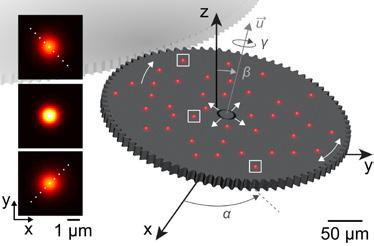
Left: Images of fluorescent particles that are above, at and below (top to bottom) the vertical position of best focus of a microscope. Calibrating the effects of lens aberrations on the apparent shape and position of the particle images enables accurate measurement of the position in all three spatial dimensions using an ordinary optical microscope. Right: Tracking and combining information from many fluorescent particles on a tiny rotating gear tests the results of the new calibration and elucidates the motion of a complex microsystem in all three dimensions. Credit: NIST
nanoscale gaps between microsystem parts, which varied due to imperfections in the fabrication of the system. Just as a loose bearing on a wheel causes it to wobble, the study showed that the nanoscale gaps between parts not only degraded the precision of the intentional rotation, but also caused unintentional wobbling, rocking and even flexing of the gear, all of which could limit its performance and reliability.
Microscopy laboratories could easily implement the new method, Copeland said. “The user just needs a standard sample to measure their effects and a calibration to use the resulting data,” added Stavis. Aside from the fluorescent particles or a similar standard, which already exist or are emerging, no extra equipment is needed. The new journal article includes demonstration software that guides researchers in how to apply the calibration.
Paper: Craig R. Copeland, Craig D. McGray, B. Robert Ilic, Jon Geist and Samuel M. Stavis. Accurate localization microscopy by intrinsic aberration calibration. Nature Communications. June 24, 2021. DOI: 10.1038/s41467-02123419-y
Source: https://www.nist.gov/news-events/news/2021/06/ escape-flatland-calibration-method-enables-microscopes-makeaccurate
Multilayer Sandwich
PTB News 2.2021 — Josephson arbitrary waveform synthesizers (JAWS) allow quantized AC voltages to be synthesized with arbitrary and spectrally pure waveforms. At PTB, a pulse-driven Josephson standard for the generation of AC voltages with series arrays has been realized. These arrays are based on stacks of up to five Josephson junctions. This new technology has allowed the integration density of the circuits – and thus their output voltage – to be considerably increased: With up to 30 000 junctions per chip, it is now possible to generate an effective voltage of 0.5 V RMS (0.7 V peak). The yield of the fabrication process has been clearly increased by adapting various parameters.
Pulse-driven Josephson AC voltage standards enable a large number of metrological applications and are based on series arrays of superconducting Josephson junctions of the kind manufactured in the Clean Room Center of PTB. In the long run, it is planned that the output voltage will be further increased to reach values between 7 V and 10 V to extend the range of possible applications.
One of the measures envisaged in order to achieve such an increase consists in raising the integration density of

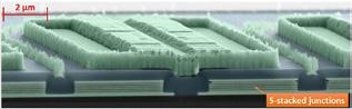
SEM image of a series array with 5 stacked Josephson junctions (cross section view). The height of the junction stacks amounts to approx. 800 nm; all layers taken together are roughly 3 μm in height. Credit: PTB in depositing 16 layers in approx. 40 individual process steps.
Contact: Oliver Kieler (oliver.kieler(at)ptb.de), Department 2.4, Quantum Electronics, Phone: +49 531 592-2410
Scientific publication: O. Kieler, R. Wendisch, R. Gerdau, T. Weimann, J. Kohlmann, R. Behr: Stacked Josephson junction arrays for the pulse-driven AC Josephson voltage standard. IEEE Trans. Appl. Supercond. 31 (2021)
Source: https://www.ptb.de/cms/en/presseaktuelles/journalsmagazines/ptb-news.html
Josephson junctions on the chips. Since the junctions are integrated into a high-frequency structure (a coplanar waveguide), the possibility to increase the length of the series array is limited. To increase the number of junctions on each chip, the junctions were stacked vertically. This was made technologically possible by the material layer combination of the Josephson junctions, which consist of Nb and Si.
After several modifications and enhancements of the standard process used at PTB, which is based on electron beam lithography, stacks of up to 5 Josephson junctions have now been successfully implemented with a high process yield. Two important process enhancements are worth mentioning in this context: For one thing, a chemicalmechanical polishing procedure was introduced for the planarization of the array surfaces. Thanks to this procedure, the successive superconducting layers can be deposited and then structured in compliance with high quality requirements (high superconducting current carrying capacity). For another, a non-conducting silicon oxide layer was deposited between the electrically conducting structures by means of atomic layer deposition (ALD) in collaboration with the Leibniz Institute of Photonic Technology (IPHT) in Jena. Contrary to the silicon oxide non-conducting layers that had previously been manufactured at PTB by means of plasmaenhanced chemical vapor deposition, ALD layers have the advantage of covering edges perfectly. They thus provide good edge isolation even at extreme aspect ratios such as those prevailing in 5-fold stacks of junction arrays.
PTB is planning to make the ALD technology available in its own Clean Room Center in the future. All in all, the complex fabrication process in which 30 000 Josephson junctions are integrated onto a chip with a surface of (10 × 10) mm2 consists
Big Berthas Used to Measure Laser Power
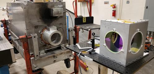
By Daryl Mayer, AFLCMC Public Affairs / Published June 29, 2021 WRIGHT-PATTERSON AFB, Ohio (AFLCMC) – The Air Force Metrology and Calibration Division is using some unique mobile "Big Bertha" series High Energy Laser primary reference calorimeters to support Air Force Research Laboratory’s national defense programs work on lasers. The HEL calibration supports the Laser Hardened Materials Evaluation Laboratory (LHMEL) of the Air Force Research Laboratory’s Materials and Manufacturing Directorate at Wright Patterson AFB and the AFRL Directed Energy Directorate at Kirtland AFB in Albuquerque, NM. For over 35 years, AFRL’s LHMEL has provided the aerospace community with a comprehensive source for high temperature characterization of current and emerging materials using a variety of infrared laser sources and environmental simulation capabilities. The calibrations performed by AFMETCAL enable LHMEL to accurately simulate high service life temperatures experienced by parts within a jet engine. The calorimeter designated Big Bertha 1 (left) will eventually be replaced by the Air Force’s new High Energy Laser standard Radiation Pressure Power Meter (right). (Courtesy photo)