5 minute read
Quantum Future
from Inside Electrical and Computer Engineering at the University of Michigan 2021
by Electrical & Computer Engineering at University of Michigan
When you push the size of a system to atomic scale, new quantum phenomena come alive. We know what they are, but we haven’t quite figured out how to control them.
Control is the next step to the ultimate goal of full integration of quantum devices with traditional semiconductor devices.
CONTROLLING THE QUANTUM FUTURE
Developing New Nano-Quantum Materials
ECE faculty and collaborators are developing a new family of III-nitride nano-quantum materials (nQMs) which are expected to contribute to future advances in quantum devices for quantum information, communication, air purification, object sterilization, and sensing. At the center of these nQMs are extreme quantum-dot arrays – called extreme because they contain just a few atoms compared to the thousands found in “normal” dots. For the project to be a success, the researchers will innovate and control these quantumdots arrays at nanoscale to produce the desired macroscopic, collective actions.
“By demonstrating the controlled synthesis of such atom clusters utilizing industry-standard processing tools, we hope to establish the material platform for scalable, next-generation quantum technology,” said project director Zetian Mi. Control is the key, and it’s very tricky business. “When you make these quantum nanostructures, new operational principles come alive,” said co-investigator Mackillo Kira. These quantum principles cause unusual things to happen when a small number of nanosized particles are confined. Called quantum effects, they don’t conform to the expectations of classical physics, but they can be predicted by quantum theory. In addition, different quantum effects sometimes come into play depending on the number of nano-quantum particles that begin to work together. Kira will be in charge of developing a systematic quantum theory that will predict the behavior of the nQMs. The newly-developed theory will enable scientists to precisely predict and determine the electronic, optical, excitonic, and entanglement properties of quantum nanostructures, and perhaps most importantly for this research - how to control quantum light. “We’re talking about controlling the energy of light, and then what type of light is emitted,” said Kira, “which is also critical for quantum information applications, such as moving information long distances, quantum processing, information security, or highly sensitive sensing and detection.” Building on the theory, Mi’s group will grow quantum nanostructures based on III-nitride semiconductors.
“This is also a wide bandgap material ideally suited for UV optoelectronics, including UV LEDs for disinfectant applications,” said Mi. “Broadly speaking, 200 to 280 nanometers is very important for disinfection purification applications. But there is no viable way to do that using conventional semiconductor technology.” Air purification and room sterilization, critical in hospital settings, are some of the key applications for Mi’s research. Current technology uses mercury lamps, a highly toxic material. In addition, Mi says that by using quantum nanostructures, as opposed to traditional semiconductors, the process can be made highly efficient. In addition to Mi and Kira, key members of the team include Professors Ted Norris and Parag Deotare, who will test and evaluate the materials, Prof. Manos Kiopakis (Materials Science and Engineering Department), who will help with the design and modeling of monolayer GaN structures, and industrial partners Sandia National Lab and the Air Force Research Lab, who bring extensive experience in materials characterization. “If we can make a few entanglement-based demonstrations, based on the new materials, that’s a big step forward,” said Kira. “That would be a founding moment of making semiconductors quantum ready.”
A new tool that uses light to map out the electronic structures of crystals could reveal the capabilities of emerging quantum materials and pave the way for advanced energy technologies and quantum computers. “Quantum materials could have an impact way beyond quantum computing,” said Prof. Mackillo Kira, who led the theory side of the new study. “If you optimize quantum properties right, you can get 100% efficiency for light absorption.” Silicon-based solar cells are already becoming the cheapest form of electricity, although their sunlight-to-electricity conversion efficiency is rather low, about 30%. Emerging “2D” semiconductors, which consist of a single layer of crystal, could do that much better—potentially using up to 100% of the sunlight. They could also elevate quantum computing to room temperature from the near-absolute-zero machines demonstrated so far.
“New quantum materials are now being discovered at a faster pace than ever,” said Rupert Huber, professor of physics at the University of Regensburg in Germany, who led the experimental work. “By simply stacking such layers one on top of the other under variable twist angles, and with a wide selection of materials, scientists can now create artificial solids with truly unprecedented properties.” The research team succeeded in measuring 2D quantum materials using a laser-based method at room temperature and pressure. The measurable operations include processes that are key to solar cells, lasers and optically driven quantum computing. Additional applications for this avenue of research, which was published in Science, include LED lights, solar cells and artificial photosynthesis.

The electrons absorb laser light and set up “momentum combs” (the hills) spanning the energy valleys within the material (the red line). When the electrons have an energy allowed by the quantum mechanical structure of the material—and also touch the edge of the valley—they emit light. This is why some teeth of the combs are bright and some are dark. By measuring the emitted light and precisely locating its source, the researchers mapped out the energy valleys in a 2D crystal of tungsten diselenide. Credit: Markus Borsch, Quantum Science Theory Lab, University of Michigan.
Information Processing Using Quantum Dot Arrays

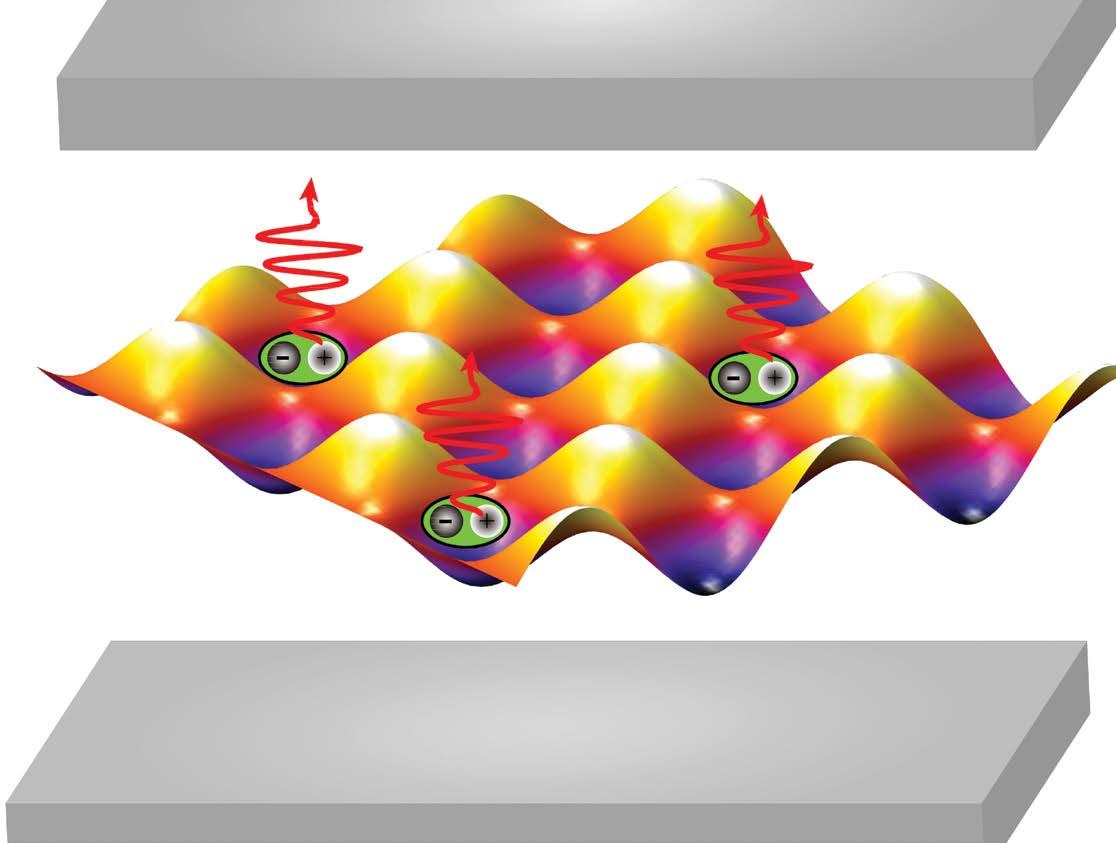
An illustration of the electronic structure. Credit: Long Zhang, Deng Lab, University of Michigan By putting a twist on new “2D” semiconductors, an international team of researchers have demonstrated their potential for using single photons to transmit information. Their experiment demonstrated the possibility of using an effect known as nonlinearity to modify and detect extremely weak light signals, taking advantage of distinct changes to a quantum system to advance next generation computing. “We are coming to the end of Moore’s Law,” said Stephen Forrest, Peter A. Franken Distinguished University Professor of Electrical Engineering, Paul G. Goebel Professor of Engineering, and key investigator on the project. “Two dimensional materials have many exciting electronic and optical properties that may, in fact, lead us to that land beyond silicon.” In order for an array of quantum dots inside a 2D semiconductor to be controlled as a group with light, the team built a resonator by making one mirror at the bottom, laying the semiconductor on top of it, and then depositing a second mirror on top of the semiconductor.
“Researchers have wondered whether detectable nonlinear effects can be sustained at extremely low power levels—down to individual photons. This would bring us to the fundamental lower limit of power consumption in information processing,” said Hui Deng, a professor of physics who directed the research. “We demonstrated a new type of hybrid state to bring us to that regime, linking light and matter through an array of quantum dots.”


