
1 minute read
1.4 ● GPIO Pinout


SW5: DAPLink adapter button. Keep this button pressed while applying power to the board to put the MAX32625 DAPLink adapter onboard to MAINTENANCE mode for DAPLink firmware updates.
The functions of the LEDs are:
D1: Connected to the MAX78000 GPIO ports. This LED can be controlled by user firmware.
Port 2_0 : Red Port 2_1 : Green Port 2_2 : Blue
D2: Connected to MAX20303 PMIC LEDx outputs. These LEDs can be controlled through I2C commands. They also can be configured as charge status indicators by issuing I2C commands.
D3: DAPLink adapter MAX32625 status LED. Controlled by the DAPLink adapter and cannot be used as a user LED.
1.4 ● GPIO Pinout
There are two headers at either side of the board where GPIO signals are terminated. As shown in Figure 1.3, Header J4 has 12 pins and Header J8 has 16 pins. The board includes the following GPIO port pins:
PORT0: P0_5, P0_6, P0_7, P0_8, P0_9, P0_11, P0_16, P0_17, P0_19 PORT1: P1_0, P1_1 PORT2: P2_3, P2_4, P2_6, P2_7 PORT3: P3_1
Tables 1.1 and 1.2 show the J4 and J8 pin names and their descriptions. Notice some pins are shared. For example, P1_0 and p1_1 are shared with the UART RX and TX pins respectively. Similarly, P2_3 and P2_4 are shared with analog inputs AIN3 and AIN4 respectively.
Table 1.1 Header J4 pins
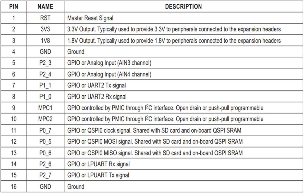
Table 1.2 Header J8 pins


