


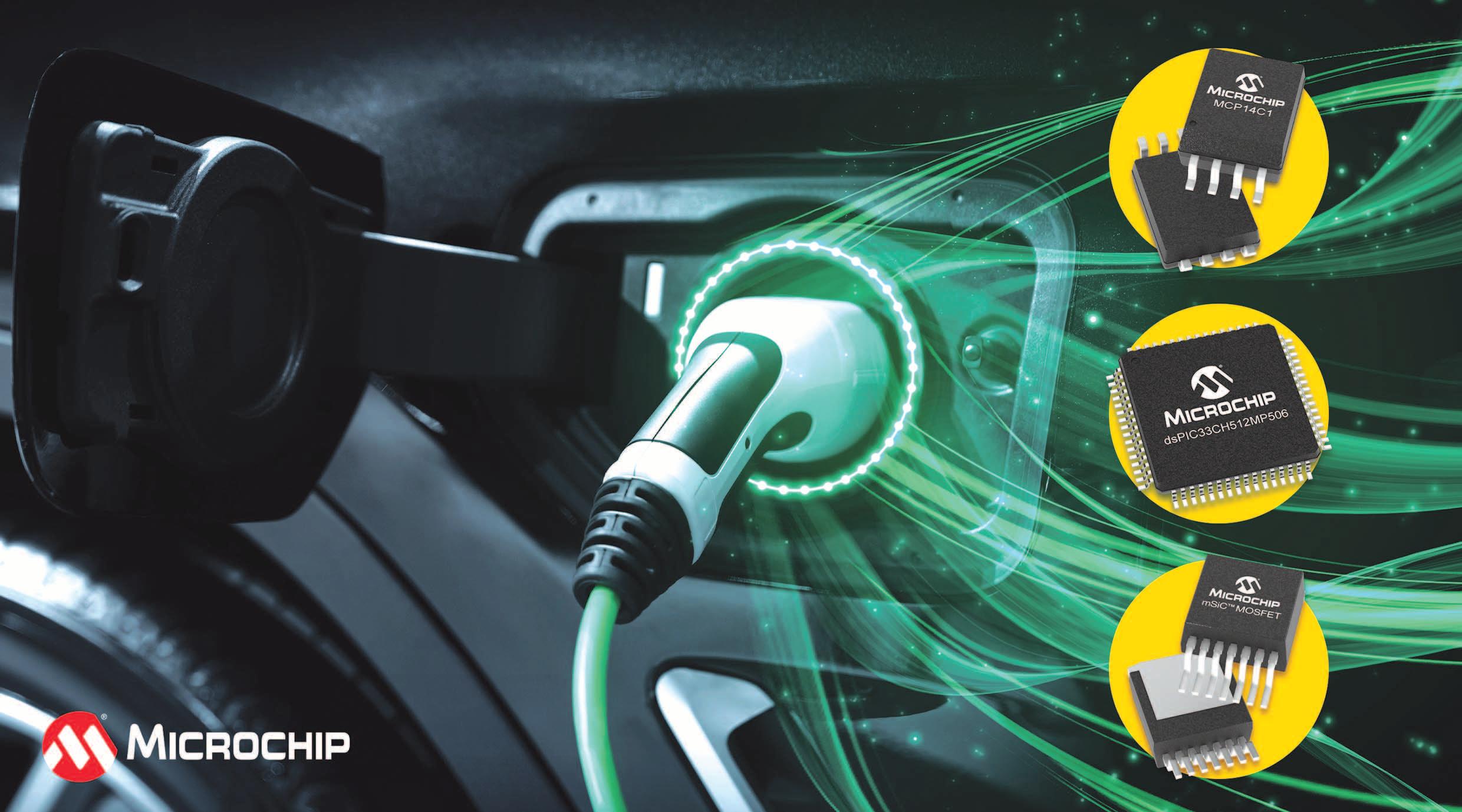
Designers can speed time to market for their on-board charger application with key technologies from one supplier, including the control, gate drive and power stage
The market for Battery Electric Vehicles (BEVs) and Plug-in Hybrid Electric Vehicles (PHEVs) continues to grow as the push towards decarbonization requires sustainable solutions to reduce emissions. A critical application for EVs is the on-board charger, which converts AC power into DC power to recharge the vehicle’s high-voltage battery. Microchip Technology today announces an On-Board Charger (OBC) solution that uses a selection of its automotive-qualified digital, analog, connectivity and power devices, including the dsPIC33C Digital Signal Controller (DSC), the MCP14C1 isolated SiC gate driver and mSiC™ MOSFETs in an industry-standard D2PAK-7L XL package.
This solution is designed to increase an OBC system’s efficiency and reliability by leveraging the dsPIC33 DSC’s advanced control functions, the MCP14C1 gate driver’s highvoltage reinforced isolation with robust noise immunity and the mSiC MOSFETs’ reduced switching losses and improved thermal management capabilities. To further simplify the supply chain for customers, Microchip provides the key technologies that support the other functions of an OBC, including communication interfaces, security, sensors, memory and timing.
To accelerate system development and testing, Microchip offers a flexible programmable solution with ready-to-use software modules for Power Factor Correction (PFC),


DC-DC conversion, communication and diagnostic algorithms. The software modules in the dsPIC33 DSC are designed to optimize performance, efficiency and reliability, while offering flexibility for customization and adaptation to specific OEM requirements.
Here is an overview of the key components in this OBC solution:
• The dsPIC33C DSC is AEC-Q100 qualified and features a high-performance DSP core, high-resolution Pulse-Width Modulation (PWM) modules and highspeed Analog-to-Digital Converters (ADCs), making it optimal for power conversion applications. It is functional, safety ready and supports the AUTOSAR®
• The MCP14C1 isolated SiC gate driver is AEC-Q100 qualified and is offered in SOIC-8 wide-body package supporting reinforced isolation and SOIC-8 narrowbody supporting basic isolation. Compatible with the dsPIC33 DSC, the MCP14C1 is optimized to drive mSiC MOSFETs via Undervoltage Lockout (UVLO) for VGS = 18V gate drive split output terminals, which simplifies implementation and eliminates the need for an external diode. Galvanic isolation is achieved by leveraging capacitive isolation technology, which results in robust noise immunity and high CommonMode Transient Immunity (CMTI).


• The mSiC MOSFET in an AEC-Q101-qualified D2PAK-7L XL surface mount package includes five parallel source sense leads to reduce switching losses, increase current capability and decrease inductance. This device supports 400V and 800V battery voltages.
Microchip has published a white paper that provides more information about how this OBC solution can optimize a design’s performance and speed up its time to market. For more information about Microchip’s OBC solutions for EVs, visit Microchip’s website
The dsPIC33C DSC is an AUTOSAR-ready device and is supported by the MPLAB® development ecosystem including MPLAB PowerSmart™ Development Suite.
The main components for an OBC solution including the dsPIC33C DSC, the MCP14C1 isolated SiC gate driver and the mSiC MOSFET in a D2PAK-7L XL package are now available. For additional information and to purchase, contact a Microchip sales representative, authorized worldwide distributor or visit Microchip’s Purchasing and Client Services website, www.microchipdirect.com.
Microchip Technology www.microchip.com
3 | Microchip Makes it Easier to Design an On-Board Charger Solution
6 | Moxa New-gen x86 Industrial Computers Recognized by “Red Dot Award: Product Design 2024”
6 | Mouser Electronics, in Collaboration with STMicroelectronics, Explores Wireless Connectivity in New eBook
7 | Infineon introduces Power System Reliability Modeling to reduce power shortages and blackouts in data center systems
8 | Nexperia’s portfolio of 650V SiC diodes now addresses automotive and a wider range of industrial applications
8 | Newest Mouser Series Navigates Zonal Architectures for Software-Defined Vehicles
9 | Vector and QNX: Cooperation for Best-In-Class Solution of Safe Systems in SDVs
10 | Reference Book on Wireless Power Transmission Expanded
10 | Anglia adds new Environmental resource hub to speed compliance and introduces Beehives to its distribution centre site
11 | WeEn Semiconductors Unveils Latest Rugged, High-Performance IGBTs

eBooks 28 | Authorized Distributor Mouser Electronics Offers Wide Range of MEAN WELL Power Solutions

Management
Managing Director - I onela G anea
Editorial Director - Gabriel N eagu
Accounting - I oana P araschiv
Advertisement - Irina G anea
Web design - Eugen Vărzaru

Contributing editors
Cornel Pazara
PhD. Paul S vasta
PhD. N orocel C odreanu
PhD. Marian Blejan
PhD. B ogdan G rămescu
| TEN 30UIR & 40UIR / THN 10UIR series
Alphawave Semi Collaborates with Arm on High-Performance Compute Chiplet

| Testing O-RAN compatible devices
43 | Introducing the TimeProvider® XT Extension System for Migrating to a Modern Synchronization and Timing Systems Architecture

| New Power Supply Concepts Needed for Intelligent Edge Sensors


Azi” is a registered trademark at OSIM - Romania, Registered position:


Moxa Inc., a leader in industrial communications and networking, celebrated its new x86 industrial computers (IPCs) family—the BXP, DRP, and RKP Series reaching the pinnacle of design excellence with the Red Dot Winner 2024 recognition in the Industrial Design category. Designed to meet most industrial automation market needs, the rugged computers are equipped with exceptional reliability, adaptability, and longevity to address the increasing demands of data connectivity and real-time processing of large volumes of sensor and device data at the industrial edge.
The new x86 industrial computers emerged victorious at the Red Dot Award: Product Design 2024, thanks to its adaptable and user-oriented design with robust housing and remarkable I/O options for easy accessibility and edge connectivity to industrial applications. “With adaptability and user-oriented design, DRP, BXP, and RKP manage the complex requirements of industrial automation,” the prestigious Red Dot Award jury stated. Industrial computers play essential roles at the industrial edge, facilitating effective communication between industrial networks and various components of automation systems. They can enable both easy configuration and flexible integration while ensuring stable data connectivity for operations, making life easier for asset owners and system integrators. Notably, the DRP-C100 and BXP-C100 Series excel in performance, resilience, and endurance, making them ideal for Battery Energy Storage Systems (BESS). These systems require efficient data logging and robust data storage to manage thousands of data points generated every minute by monitoring systems, ensuring accurate data for maintenance and warranty claims. Engineered to maximize capabilities for industrial edge connectivity, the BXP, DRP, and RKP Series are each backed by a robust 3-year hardware warranty and 10-year longevity commitment (for product released in 2023 and after). These products reaffirm Moxa’s dedication to delivering exceptional product quality and ensuring stable, long-term support for our customers’ evolving business needs. Furthermore, the simplified configure-to-order service (CTOS) enables customers to identify the best fit for their applications in just a few steps.
■ MOXA | https://moxa.com

, Inc., the New Product Introduction (NPI) leader empowering innovation, today announces a new eBook in collaboration with STMicroelectronics, offering an in-depth look at wireless connectivity.
The plethora of new and pre-existing connected Internet of Things (IoT) and Industrial Internet of Things (IIoT) devices, gateways, and sensors require that wireless technology be dependable and compatible with many wireless protocols. This need will only grow as more technologies, such as connected vehicles, medical and wearable devices, and wireless charging fully mature. In Beyond the Wires: Exploring Bluetooth and LoRaWAN Connectivity, experts from STMicroelectronics discuss the evolution of the Bluetooth® Low Energy and LoRaWAN wireless standards and their benefits.
The eBook offers many use cases, from remote sensor networks to smart cities and homes, from agriculture to public entertainment. Special requirements for security, private networks, long-range and more are also discussed. The eBook also highlights relevant products from STMicroelectronics, including the company’s industry-leading RF system-on-chip (SoC) solutions, modules and development tools.
The STM32WBA5 multiprotocol wireless radio microcontroller (MCU), available from Mouser, features a powerful

Arm® Cortex®-M33 core and is certified for the Bluetooth Low Energy 5.4 protocol, Zigbee® R23 and OpenThread® 1.3. The STM32WBA5 offers an ultra-low-power platform and inherited digital/analogue peripherals, suitable for many applications, from industrial to smart home and consumer markets.
The STM32WLE5 wireless long-range microcontroller embeds a powerful and ultra-low-power LPWAN radio solution consisting of LoRa®, (G)FSK, (G)MSK, and BPSK. The Arm core of this MCU implements a full set of DSP instructions and an independent memory protection unit (MPU) that enhances application security.
The NUCLEO-WBA55CG Nucleo-64 board eases prototyping applications with the STM32WBA5 wireless microcontroller. Arduino Uno V3 connectivity support and ST morpho headers allow functionality expansion with a wide choice of specialised shields.
The STEVAL-ASTRA1B evaluation board includes LoRa, Bluetooth LE, and NFC, as well as a GNSS positioning module and MEMS sensors (including temperature and pressure sensors, an accelerometer, and a gyroscope), making it a complete proof-of-concept for asset tracking and monitoring.
The STEVAL-PROTEUS1 evaluation board includes Bluetooth LE, MEMS sensors and secure elements to target Industry 4.0 applications with condition-based maintenance and predictive maintenance, including the capability of anomaly detection thanks to AI capability.
The STM32WBA55G-DK1 Discovery kit is a complete demonstration and development platform for the STM32WBA55CGU7 MCU, enabling a wide diversity of applications by exploiting low-power communication, the Bluetooth SIG isochronous channel feature related to audio capability for Bluetooth Low Energy Audio, Matter as Border Router, and Zigbee.
To learn more about STMicroelectronics, visit: https://eu.mouser.com/manufacturer/stmicroelectronics.
To read the new eBook, visit: https://resources.mouser.com/manufacturer-ebooks/stbeyond-the-wires-bluetooth-lorawan-connectivity.
■ Mouser Electronics | www.mouser.com



Infineon Technologies AG introduces Power System Reliability Modeling, an innovative solution addressing the increasing challenges faced by data centers and telecom infrastructures due to power supply failures in the system. With 39 percent of downtimes attributed to power outages and an average cost of $687,700 per downtime, the need for seamless operations and mitigation of financial impact is urgent. By integrating Infineon’s power monitoring solution, organizations can enhance operational resilience, reduce their carbon-footprint and achieve substantial cost savings. The offering consists of an algorithm running on a digital power controller, thus integrating software and hardware. This is in line with Infineon’s strategic approach to provide customers with comprehensive system solutions that include both semiconductor devices and matching software tools. Target applications of the solution include DCDC converters, ACDC rectifiers and IBC modules utilized in data centers, AI servers, GPUs, and telecom networks. Power System Reliability Modeling acts as a bridge between component and system reliability. It enables real-time power supply health monitoring of the system and lifetime estimation based on dynamic system operating parameters, a power supply system model, and a reliability prediction procedure in digital power controllers by Infineon. This solution ensures improved device utilization and data-driven maintenance recommendations, translating into enhanced profitability and reduced Total Cost of Ownership (TCO). Customers benefit from real-time system diagnostics for their power supply as well as powerful system reliability-based decisions and quality assurance. The solution is easy to use and integrate into existing designs.
Further information about the solution is available at www.infineon.com/reliabilitymodeling.
■ Infineon Technologies | www.infineon.com

Nexperia’s portfolio of 650V SiC diodes now addresses automotive and a wider range of industrial applications
Nexperia announced that its class-leading 650 V, 10 A silicon carbide (SiC) Schottky diode is now automotive qualified (PSC1065H-Q) and available in real-two-pin (R2P) DPAK (TO252-2) packaging, making it suitable for various applications in electric vehicles and other automobiles. Additionally, in a further extension to its portfolio of SiC diodes, Nexperia is now also offering industrial-grade devices with current ratings of 6 A, 16 A, and 20 A in TO-220-2, TO-247-2, and D2PAK-2 packaging to facilitate greater design flexibility. These diodes address the challenges of demanding high voltage and high current applications including switched-mode power supplies, AC-DC and DC-DC converters, battery-charging infrastructure, motor drives, uninterruptible power supplies as well as photovoltaic inverters for sustainable energy production.
The merged PiN Schottky (MPS) structure of these devices provides additional advantages over similar competing SiC diodes, including outstanding robustness against surge currents. This eliminates the need for additional protection circuitry, thereby significantly reducing system complexity and enabling hardware designers to achieve higher efficiency with smaller form factors in rugged high-power applications. Nexperia’s consistent quality across various semiconductor technologies provides designers with confidence in the reliability of these diodes.
In addition, Nexperia’s ‘thin SiC’ technology delivers a thinner substrate (one-third of its original thickness) which dramatically reduces the thermal resistance from the junction to the back-side metal. This results in lower operating temperature, higher reliability and device lifetime, higher surge current capability, and lower forward voltage drop.
To learn more about Nexperia’s extended range of 650 V SiC Schottky diodes for automotive and industrial applications, visit www.nexperia.com/sic diodes.
■ Nexperia | www.nexperia.com

As automotive technology ratches up in electronics, designers have turned to zonal architecture — to maximize efficiency within individual subsystems while allowing for easier management of the hardware and software stacks for the whole car.
Mouser Electronics, Inc., the authorized global distributor with the newest electronic components and industrial automation products, today announced the newest installment of its Empowering Innovation Together (EIT) technology series, which examines the benefits of zonal architectures and the enhanced connectivity features it provides software-defined vehicles (SDV). This installment of the EIT technical content series explores design concepts, virtualization, and future use cases enabled by zonal architectures, driving future automotive innovations.
As the automotive industry shifts towards electric vehicles and advanced driver assistance systems, these modern designs require significant hardware and software upgrades.

Vehicle performance is optimized by creating distinct zones within the vehicle that cater to specific functionalities and implementing vehicle compute platforms. This approach offers improved reliability, increased performance, and longer lifespans for cars, ultimately transforming them into immersive experiences. Mouser explores how these new features can open up a plethora of possibilities for automotive design and engineering.
Join The Tech Between Us podcast, where Mouser Director of Technical Content Raymond Yin and Christian Uebber, Chief Technology Officer from ETAS, discuss the complex nature of advanced architectures. Together, they explore the necessary software and hardware changes to transition to new compute platforms, with emphasis on the importance of codesign considerations.
“In our latest spotlight, we explore the transformative possibilities of zonal architecture,” said Yin . “This forward-looking approach is revolutionizing spatial design, and we delve into its variety of applications through insightful discussions with leading experts in the field.”
This series includes technical articles, an infographic, a video and more, introducing the SDV movement and how zonal architectures enhance safety, efficiency, and personalization. These resources offer guidance to automotive engineers who are considering the benefits of this new network architecture.
Established in 2015, Mouser’s Empowering Innovation Together program is one of the industry’s most recognized electronic component programs.
To learn more, visit https://www.mouser.com/empoweringinnovation and follow Mouser on Facebook, LinkedIn, X and YouTube
■ Mouser Electronics | www.mouser.com


Vector announces a collaboration with QNX, a business unit of BlackBerry Limited, that will pave the way to Automotive Safety Integrity Level (ASIL) D for SoftwareDefined Vehicles (SDV).
Within the collaboration, Vector provides a QNX® operating system (OS) integration, the corresponding interface and a safety case. OEMs and Tier-1s can now easily develop AUTOSAR-based applications with MICROSAR Adaptive Safe on QNX® OS for Safety while benefiting from pre-aligned and industry-certified safety concepts to create safe, highperformance systems for SDVs.
“This collaboration is an important step towards realizing the Software-Defined Vehicle,” says Grant Courville, Vice President of Product and Strategy at BlackBerry QNX. “We are working closely with Vector to deliver a pre-integrated offering that realizes the benefits of the QNX OS for Safety combined with MICROSAR Adaptive Safe for our mutual customers.”
While integrating AUTOSAR Adaptive to the QNX OS, performance is always a key requirement at Vector. Therefore, to address these performance needs, a specific QNX OS abstraction layer was developed that makes use of native QNX API system calls.
“Partnering with innovators such as QNX enables our customers to develop faster and more efficiently,” says Matthias Traub, Director Embedded Software and Systems at Vector. “We accelerate the development of SDVs with pre-integrated and coordinated and industry-certified safety concepts”.
For more information on Vector’s SDV solutions, visit: www.vector.com/sdv
■ Vector | www.vector.com

Reference book “Trilogy of Wireless Power Transfer”: Expertise for wireless power transmission Image source: Würth Elektronik
The reference book “Trilogy of Wireless Power Transfer” by Würth Elektronik is now available in a revised second edition. The manufacturer with the largest selection of wireless power coils on the market shares its expertise in wireless power transmission. The practice-oriented reference book consists of three parts: Basic Principles of Wireless Power Transmission, Wireless Power Transfer Systems and Applications. It costs 19 euros and is available from Würth Elektronik and in bookstores.
The first part of the reference book has been completely revised and explains the physical principles of the various methods of contactless power transmission. The key standards and developments of the technology are also discussed. The second part describes the wireless power transfer systems and the different topologies of wireless power transmission. In the same chapter, the correct selection of the required transmitter and receiver coils to increase efficiency, and also the available transistors, are discussed.
The practice-oriented third part is supplemented with an innovative application: NFC communication together with wireless power transmission. An overview of EMI-related topics rounds off the compilation of application examples in the practice section. The authors of the “Trilogy of Wireless Power Transfer” are Cem Som, Vice President Europe at Wurth Electronics Midcom Inc. and Dr. Michael de Rooij, Vice President Applications Engineering at Efficient Power Conversion Corporation, Inc.
■ Würth Elektronik eiSos | www.we-online.com

hub to speed compliance and introduces Beehives to its distribution centre site
Anglia Components announced a new environmental resource hub on its UK and European eCommerce platform, www.anglia-live.com, which aims to provide environmental information on each of its supply partners in one place. This will reduce the time buyers and compliance engineers are required to spend on compliance documentation when analysing supply chains to determine their own corporate environmental impact and ethical status. For each of Anglia’s authorised supply partners the hub provides links to various environmental and ethical statements, such as the manufacturer’s environmental policy, its position on conflict materials, REACH, Modern Slavery and EU sanctions against Russia.

Environmental Policies; Conflict Materials; REACH; Modern Slavery; EU Sanctions vs Russia
Anglia is highly committed to improving the environment and reducing its carbon footprint. A raft of measures have been introduced over the past 18 months, including:
• New packaging which reduces waste and is both reusable and recyclable
• Reduced air miles for components
• Smart building practices
• Environmentally friendly company transport policies
And most recently to align with its other sustainable practices and to support elements of their ISO14001 accreditation, Anglia also integrated 5 beehives into its 2 acre landscaped distribution centre site. The introduction of bees helps in maintaining a healthy balance within the local ecosystem by pollinating plants, ensuring their reproduction, and aiding in the overall sustainability of the surrounding environment.
Visit www.anglia-live.com to view the new environmental resource hub and find out more about how Anglia are demonstrating their commitment to sustainability and the environment.
■ Anglia Components PLC | www.anglia-live.com


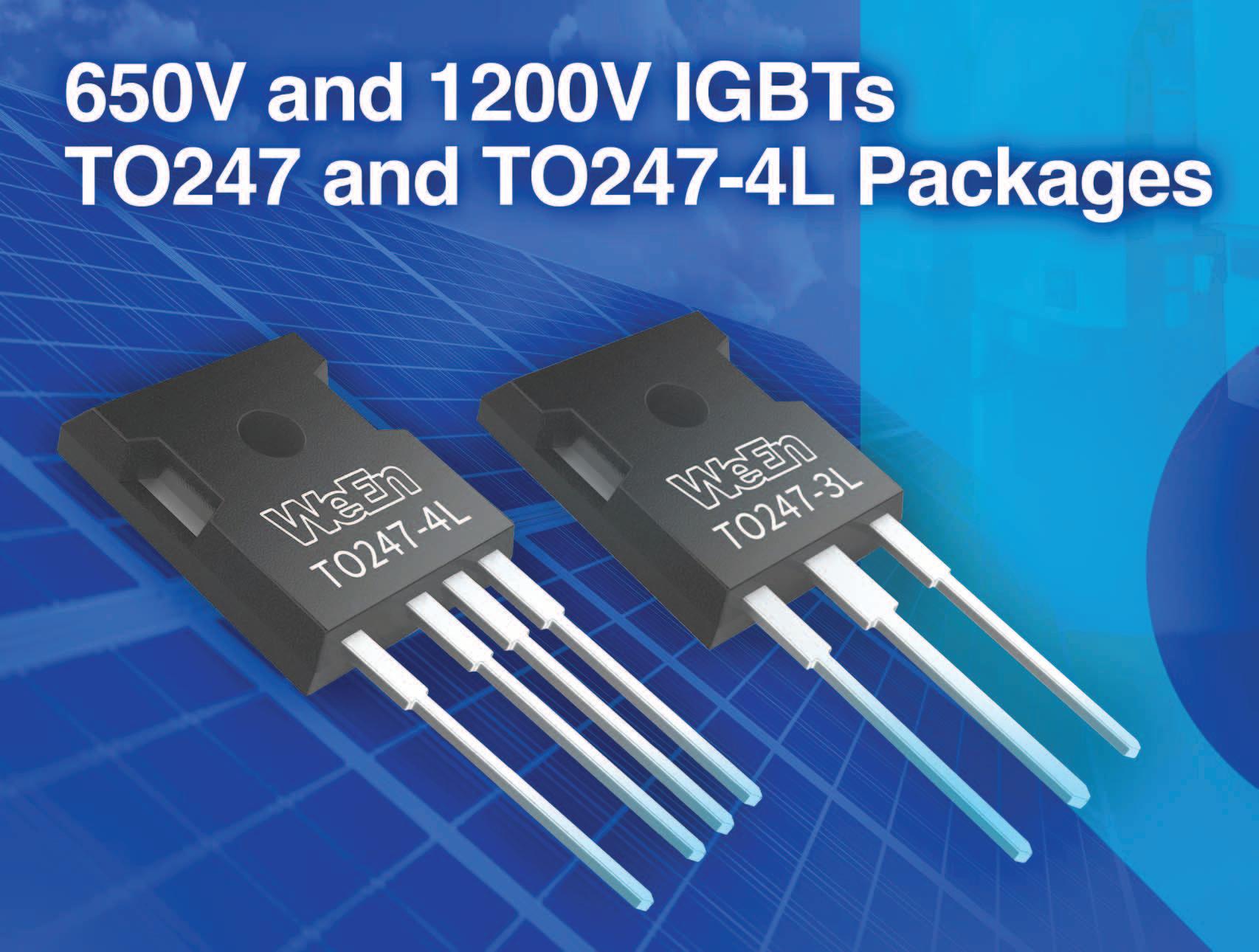
WeEn Semiconductors Unveils Latest Rugged, High-Performance IGBTs
WeEn Semiconductors, specialists in developing and manufacturing advanced bipolar power semiconductor products, has announced an expansion to its range of high-performance and rugged IGBTs at this year’s PCIM Europe exhibition and conference. Offering voltage ratings of 650V and 1200V, the new devices incorporate a fast recovery anti-parallel diode and boast extremely low leakage currents and exceptional conduction and switching characteristics at both high and low junction temperatures.
Based on an advanced fine trench gate field-stop (FS) technology, the new IGBTs provide a more uniform electric field within the chip, support higher breakdown voltages and offer improved dynamic control. By offering the optimum trade-off between conduction and switching losses, as well as an enhanced EMI design, the devices will maximize efficiency in a wide variety of mid- to high-switching-frequency power conversion designs.
The new IGBTs offer ratings of 650V/75A, 1200V/40A and 1200V/75A and are supplied in TO247 or TO247-4L packages depending on the selected device. All of the devices will operate with a maximum junction temperature (Tj) of 175 °C and have undergone high-voltage H3TRB (high-humidity, high-temperature and high-voltage reverse bias) and 100%biased HTRB (high-temperature reverse bias) tests up to this maximum.
Target applications for the new WeEn IGBTs include solar inverters, motor control systems, uninterruptible power supplies (UPS) and welding. A positive temperature coefficient simplifies parallel operation in applications where higher performance is required, while options for bare die, discrete and module product variants provide flexibility for a wide variety of target designs.
For more information, please explore WeEn Semiconductors’ product portfolio here.
■ WeEn Semiconductors | www.ween-semi.com/en

 Authors:
Pramit Nandy and Vijay Bapu Microchip Technology Inc
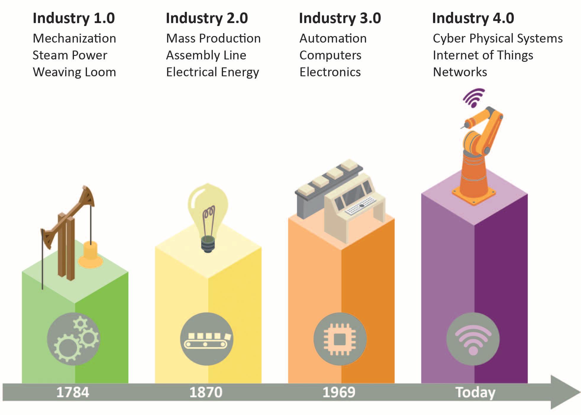
The manufacturing industry has been evolving for over 200 years now. Industry 4.0 is the fourth industrial revolution concentrating on interconnectivity, automation, machine learning, and real-time data processing. As various manufacturing industries are marching towards Industry 4.0, to stay competitive and reduce manufacturing costs, manufacturers are putting more equipment and less people in factories. Manufacturers are investing heavily in advanced mobile robotics in their factories (i.e., Amazon delivery warehouses, assembly lines) and warehouses for doing the lion’s share of the building, assembling and transporting of material. However, these mobile robots must be charged regularly which is an increasing challenge for industrial factories. There have now been some improvements in the wireless charging space that are making these robots more flexible, which has boosted the manufacturing capacity and efficiency of factories.

With the right combination of component selection, coil design and board layout, wireless charging is becoming a game changer for the manufacturing industry and is impacting the whole economy.

The latest wireless charging solutions use techniques based on the principle of electromagnetic induction. When an alternating current is passed through an induction coil on the transmitter side, an oscillating magnetic field is created. When this oscillating magnetic field couples with an induction coil on the receiver side, an alternating electric current is produced in the receiver side coil (see Figure 2).
Wireless charging systems require a number of components including the transmitter coil, tuning capacitors, a coil drive and a receiver coil. Other components include diode rectifiers, a DC-DC converter, transmitter and receiver control circuitry and algorithms, and a battery charging circuit.
In the example shown below, electromagnetic induction enables the wireless charging systems to transfer energy from a charging source pad installed on the factory floor to a receiving pad installed on the mobile robot.
Modern wireless charging systems with increased efficiency and cost-optimized components have proven to be a game changer in a factory setup for a number of reasons. First, they improve productivity and reduce manufacturing costs in a variety of ways. They enable continuous operation with opportunity charging (i.e., using idle time to charge), and reduce investment since robots can be multipurposed for different operations. They also reduce human intervention because the charging process can be automated, as well as maintenance costs since connector and cables, etc., can be eliminated resulting in a completely contactless solution.
Second, these charging systems increase safety and security. They remove the risk of sparks caused by connectors and short circuits due to contamination or moisture inside them. Other safety benefits include these solutions’ reliable detection of metal debris and other foreign objects between the transmitter and receiver coil.
Additionally, it is easy to implement secure authentication between charger and robot to avoid unauthorized access, and data transfer during charging can be used for predictive maintenance to prevent downtime. Other benefits include how much easier
wireless charging systems are to maintain and clean on the factory floor when compared to wired charging systems. This is an important contributor to the completely automated factory, minimizing human intervention and helping to create a safer environment by preventing worker-toworker spread of communicable diseases such as COVID-19).
Keeping its advantages in mind, wireless charging technology on a factory setup has the potential to take the manufacturing industry to the next level and solve difficult production challenges. However, there are some challenges with wireless charging, too. These challenges include the need for a relatively high investment to implement the wireless charging infrastructure when compared to traditional wired charging, and comparatively lower efficiency, EMI concerns. There are also safety issues related to overheating if there is a foreign object between the transmitter and receiver coil. BOM cost management and component selection are particularly important.
In the wireless power transmitter, the critical loop for the switching currents in a high-power wireless power system includes the power switches, the resonant capacitors and the coil.



This loop involves high voltages, high currents, and high switching frequencies. PCB Layout, component placement and routing in this high-power wireless power transfer system affects efficiency, EMI performance, and thermal dissipation which in turn affect system performance and reliability. There are also challenges with coil parameter variation due to manufacturing variabilities in the coil. Coil to coil variation can result in variations across products resulting in inconsistent behavior and unreliable performance in the field.
While general-purpose devices can be used to build a wireless charging solution, they cannot perform at the same level as fixed-function alternatives. Solutions can also vary in cost and efficiency depending on component selection and board layout decisions. There are many ways to optimize today’s wireless charging solutions.
Fixed-function devices are used to optimize a wireless charging solution so it can address the challenges of implementing safe, reliable, efficient wireless power at high power levels. An important step is to optimize the solution’s transmitter and receiver circuitry
that runs highly specialized algorithms for communications, power control and Foreign Object Detection (FOD). These algorithms are based on extensive R&D and multiple granted patents.
Ideally, the communication in the wireless charging solution should be in-band, eliminating the added system cost of out-ofband communications schemes. Look for power transfer frequency in the range of about 100KHz. Power control should be performed using variable frequency and variable duty cycle control of the PWM driving the full bridge inverter in the transmitter. At high power levels, FOD becomes critical. In this method, power transfer is briefly stopped for a few microseconds and the coil voltage is measured using the solution’s high peripherals and core. The presence (or not) of a foreign object can be detected by calculating the slope of the coil voltage when the output FETs are off. All components of the solution, including the controller, FETs, regulators, and coils, must be chosen such that their cost fits within the total system budget, which may need to include high-end metal contacts for reliability in an environment with moisture or dust. The efficiency of the solution depends on both the power control scheme and an optimal coil design. An
example is Microchip’s WP300 solution, whose design delivers greater than 90 percent efficiency at loads above 100 Watts. This efficiency is measured from the DC input to the transmitter to the regulated DC output of the receiver. The solution can operate at an input voltage of 12-36V DC and can regulate to a similar voltage range on the receiver side.
The PCB Layout, component placement and PCB stack-up in the WP300 based reference solution have been optimized for best performance. The PCB is designed such that the digital section, the analog and the power sections are isolated, so the noise coupling is minimized.
EMI is also mitigated using appropriate control methods in the transmitter and optimal use of decoupling capacitors to reduce switching noise, in addition to reduction in the switching frequency. Decoupling capacitors reduce the switching noise coupling but increases loss which results in increased thermal dissipation and loss in efficiency. These tradeoffs are crucial to evaluate to optimize the design. The coil parameters can be calibrated during assembly on the production line. The benefit of the solution is that coil calibration data is written to the WP300TX IC during product test.

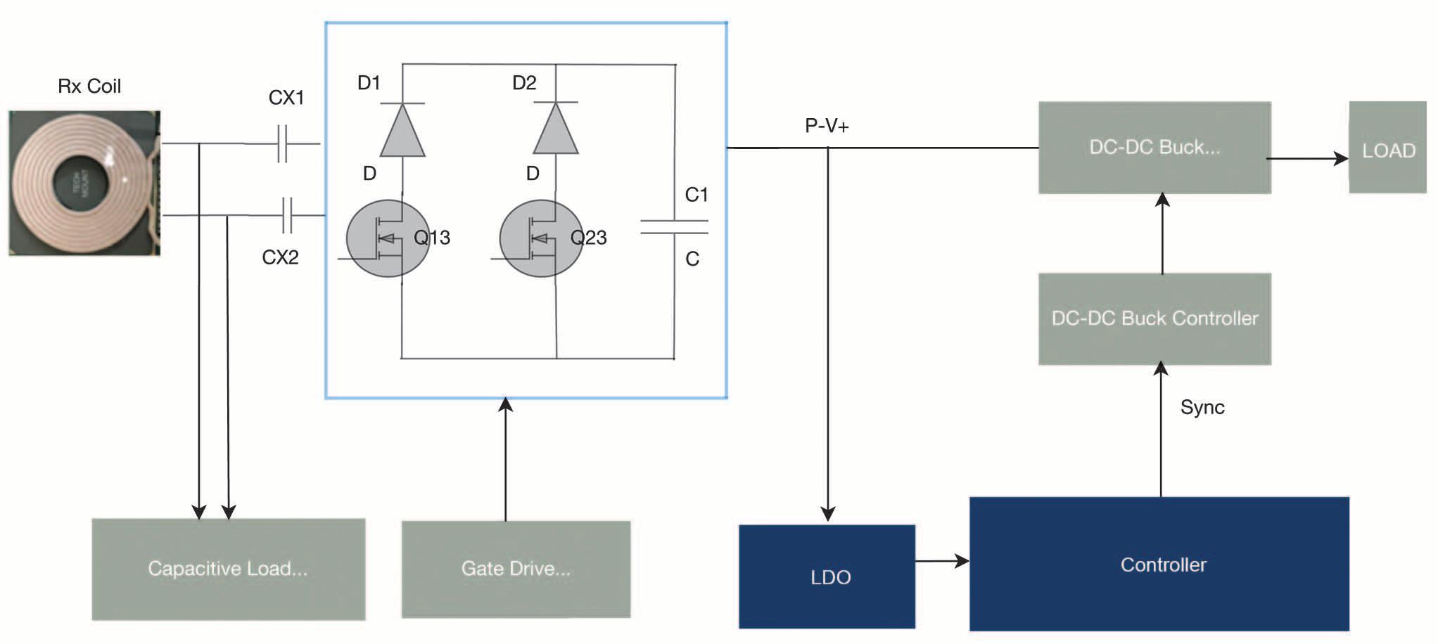
This results in consistent operation across product and reliable performance. Finally, to create 1:1 pairing between the transmitter and receiver, secure communications can be included in-band to make sure only receiver devices that are authenticated by the transmitter are powered. Figure 4 includes block diagrams of a 300W transmitter controller and 300W receiver controller that have been optimized to deliver these capabilities.


System developers should work with a supplier that provides detailed guidelines for using their wireless charging solutions including component selection, coil design and board layout.
Suppliers should also provide step-by-step guidance to ensure seamless execution of the final product. With this approach, developers can save time, mitigate risk, and simplify their wireless charger designs


so that they deliver on the full promise of electromagnetic induction technology, while also improving their productivity, reducing manufacturing cost and improving safety and security.
■ Microchip Technology www.microchip.com


World-leading performance over temperature enables cool-running, fast-switching 650 V and 1,200 V SiC MOSFETs to support up to 3x more powerful AI data centers and faster charging EVs
Navitas Semiconductor, the industry leader in next-generation GaNFast™ gallium nitride (GaN) and GeneSiC™ silicon carbide (SiC) power semiconductors, announces their new portfolio of Gen-3 ‘Fast’ (G3F) 650 V and 1,200 V SiC MOSFETs optimized for fastest switching speed, highest efficiency, and increased power density for applications such as AI data center power supplies, on-board chargers (OBCs), fast EV roadside super-chargers, and solar / energy-storage systems (ESS). The broad portfolio range covers industrystandard packages from D2PAK-7 to TO247-4, designed for demanding, highpower, high-reliability applications.
The G3F family is optimized for highspeed switching performance, resulting in 40% improvement to hard-switching figures-of-merits (FOMs) compared to competition in CCM TPPFC systems. This will enable increasing the wattage of nextgeneration AI power supply units (PSUs) up to 10 kW, and power per rack increase from 30 kW to 100-120 kW.
The G3F GeneSiC MOSFETs are developed using a proprietary ‘trench-assisted planar’
technology. and offer better-than-trench MOSFET performance, while also providing superior robustness, manufacturability and cost than competition. G3F MOSFETs deliver high-efficiency with high-speed performance, enabling up to 25°C lower case temperature, and up to 3x longer life than SiC products from other vendors.
The ‘trench-assisted planar’ technology enables an extremely low R DS(ON) increase versus temperature, which results in the lowest power losses across the complete operating range and offers up to 20% lower RDS(ON) under real-life operation at high temperatures compared to competition.
Additionally, all GeneSiC MOSFETs have the highest-published 100%-tested avalanche capability, 30% longer short-circuit withstand time, and tight threshold voltage distributions for easy paralleling, GeneSiC MOSFETs are ideal for highpower, fast-time-to-market applications.
Navitas’ latest 4.5 kW high-power density AI Server PSU reference design in CRPS185 form-factor, showcases the 650
V-rated, 40mOhms G3F FETs for an Interleaved CCM TP PFC topology. Alongside the GaNSafe™ Power ICs in the LLC stage, a power density of 138 W/inch3 and peak efficiency above 97% is realized, which comfortably achieves ‘Titanium Plus’ efficiency standards, now mandatory in Europe.
For the EV market, 1,200 V/34 mOhm (G3F34MT12K) G3F FETs enable Navitas’ new 22 kW, 800V Bi-Directional OBC and 3KW DC-DC converter to achieve a superior power density of 3,5 kW/L and a peak efficiency of 95.5%.
“G3F sets a new standard for efficient, coolrunning SiC performance, coupled with high reliability and robustness for highpower, high-stress systems,” noted Dr. Sid Sundaresan, Senior Vice President of SiC Technology and Operations. “We’re pushing the boundaries of SiC, with up to 600 kHz switching speeds, and hard-switching figures-of-merit up to 40% better than competition.”
Navitas Semiconductor www.navitassemi.com


This article focuses on the Analog Devices MAX15258, which is designed to accommodate up to two MOSFET drivers and four external MOSFETs in single-phase or dual-phase boost/inverting-buck-boost configurations. It is possible to combine two devices for triple-phase or quad-phase operation, achieving higher output power and efficiency levels.
Author: Rolf HornInginer de aplicații
DigiKey
The telecommunications sector has become an important element of modern society and instantaneous global communication. Whether for a phone call, text message, or web command, telecom equipment ensures reliable connections. The power supply operating behind the scenes is an essential component that is rarely acknowledged.
MEETING THE NEED OF INCREASED POWER DEMAND
The power demand within the telecommunications industry has grown over time, driven by developments in technology,

heightened network traffic, and the expansion of telecommunications infrastructure. The transition from third generation (3G) to fourth generation (4G) and fifth generation (5G) networks has led to advanced and high power equipment. The deployment of 5G technology has had a significant impact on the power requirements of base stations and cell towers. Base stations, particularly those in urban areas, require higher power levels to support the increased number of antennas and radio units needed for massive MIMO (Multiple Input, Multiple Output) configurations and beamforming.
Redundancy is another crucial factor. Power supplies must be designed with redundancy in mind, often including backup power sources like batteries or generators to ensure uninterrupted operation in case of power outages.
Compared to previous generations of wireless networks, the deployment of 5G mobile technology introduces several changes to power device requirements. For 5G to deliver on its promise of reliable, high speed, and low latency communication, some criteria must be addressed.
POWER AMPLIFIER REQUIREMENTS
• Support a broad spectrum of frequency bands, including sub-6 GHz and mmWave (millimeter wave) frequencies, which present unique challenges for signal propagation.

• Accommodate wider signal bandwidths and higher power levels, as well as providing linear amplification to prevent distortion of high-data-rate signals.
• Operate efficiently to minimize power consumption and heat generation, especially for battery-powered devices and remote small cells.
• Include a lightweight, compact form factor that can fit into small enclosures, such as small cell sites and user equipment.
• Incorporate advanced materials and technologies such as semiconductor devices made of Gallium Nitride (GaN) and Silicon Carbide (SiC) to provide increased power density, enhanced performance, and increased operating frequencies.
For historical, practical, and technical reasons, telecom systems typically utilize a48VDC power supply. In the event of a grid malfunction or other emergency, telecommunications networks require dependable backup power sources.


Commonly used for reserve power, leadacid batteries can also operate at -48VDC Using the same voltage for both primary and backup power makes it easier to design and maintain backup systems. Additionally, lower voltages such as -48VDC are safer for personnel working with telecom equipment, reducing the risk of electrical shock and injury. Power supplies for telecommunications equipment must meet specific operational requirements to ensure reliability and efficiency.
Here are some important specifications:
• Input voltage range: The power supply should be designed to tolerate a broad input voltage range.
• Voltage regulation: The power supply must provide a stable and regulated output voltage per the requirements of the telecom equipment.
• High efficiency: Power supplies should be highly efficient to reduce power loss and energy consumption. Efficiencies of at least 90% are typical.
• Redundancy: To ensure uninterrupted operation, power supplies frequently include redundancy features such as N+1 where an additional power supply is used. If one fails, the other can assume the burden.
• Hot-swappable: In mission-critical installations, power supplies should be hot-swappable, assuring minimal downtime during replacement or maintenance.
• High reliability: The power supply should be equipped with protection mechanisms to avert damage caused by adverse operating conditions, such as overcurrent, overvoltage, and short-circuits.
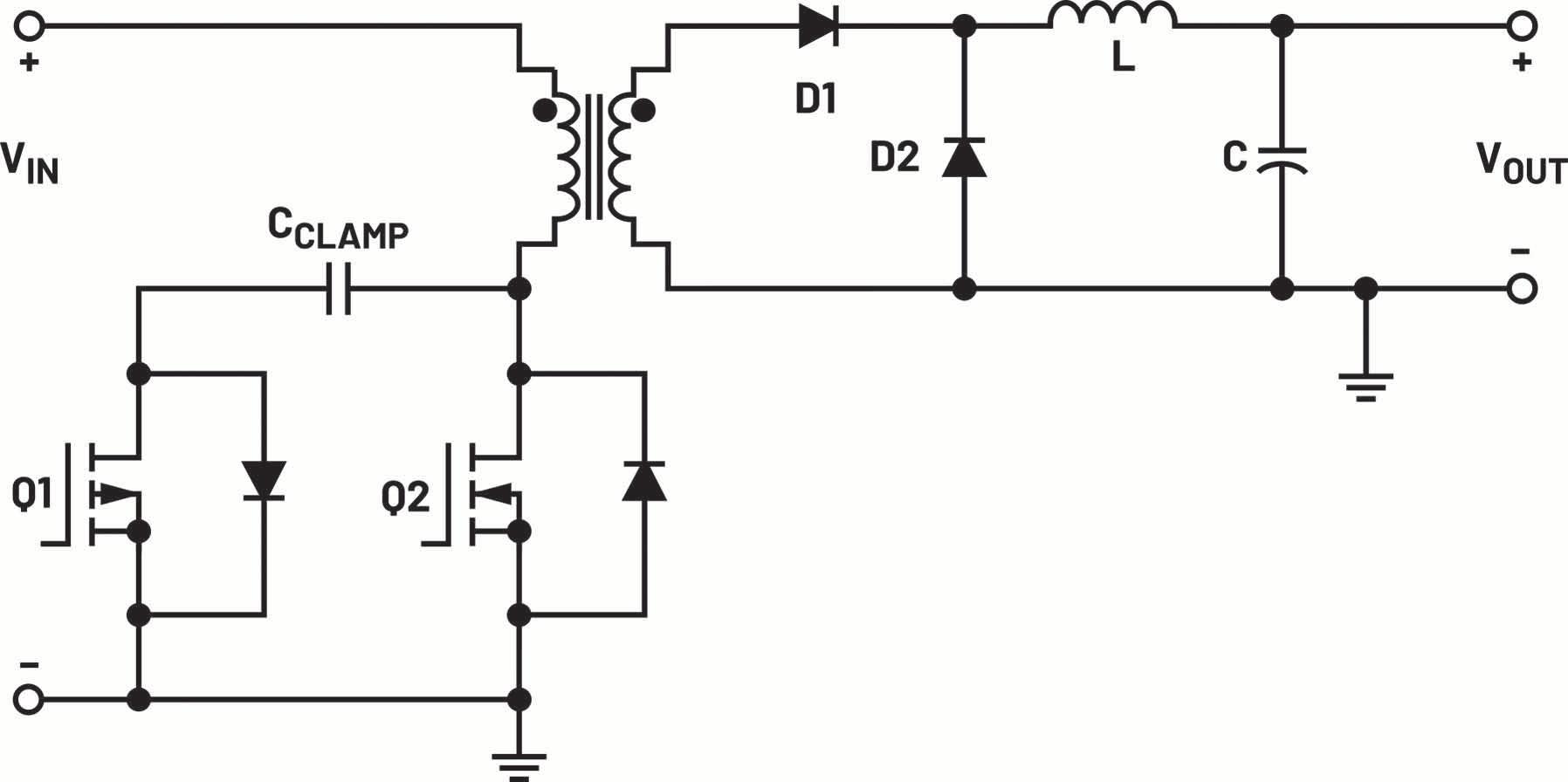
The active-clamp forward converter (ACFC) is a DC/DC converter configuration common in power supply systems, and it is primarily utilized for converting48V DC to positive voltage levels. The ACFC is a voltage conversion circuit that integrates characteristics from the forward converter and the active-clamp circuit to enhance efficiency.
This technology is prevalent in power supply systems for telecommunications and data center apparatus. The central element of the ACFC is a transformer (Figure 1).


Block diagram of a power supply stage for 5G applications.

The main winding of the transformer receives the input voltage, resulting in the induction of a voltage in the secondary winding. The output voltage of the transformer is determined by its turn ratio.
The active-clamp circuit, which incorporates supplementary semiconductor switches and a capacitor, regulates and governs the energy contained inside the leakage inductance of the transformer. When the primary switch is off, the energy stored in the leakage inductance is redirected to the clamp capacitor, thereby preventing voltage spikes. This practice mitigates the strain on the primary switch and enhances operational effectiveness. The voltage from the transformer’s secondary winding is rectified by a diode, and the output voltage is smoothed by an output filter capacitor. Finally, ACFC operates with soft switching, meaning that switching transitions are smoother and produce less noise. This results in reduced electromagnetic interference (EMI) and lower switching losses.
The ACFC circuit reduces voltage spikes and stress on components, leading to improved efficiency, especially at high input-to-output voltage ratios. Moreover, it can handle a wide range of input voltages, making it suitable for telecom and data center applications with varying input voltages.
Disadvantages of the active clamp circuit include the following:
• If not constrained to a maximum value, an increased duty cycle can result in transformer saturation or additional voltage stress on the main switch, necessitating the precise sizing of the clamp capacitor.
• ACFC is a single-stage DC-to-DC converter. As the power level rises, the advantages of a multiphase design for power intensive applications such as telecom will increase.
• An active clamp forward design cannot be scaled to higher output power and maintain similar performance.
© ADI
Analog Devices’ MAX15258 is a highvoltage multi-phase boost controller with an I2C digital interface designed for telecom and industrial applications. The device features a wide input voltage range of 8V to 76V for boost configuration and -8V to -76V for inverting buck/boost configuration. The output voltage range, from 3.3V to 60V, covers the requirements of various applications, including telecom devices.
A typical application of this versatile IC is the power supply for a 5G macrocell or femtocell shown in Figure 2.


The hot-swap feature is ensured by a negative voltage hot-swap controller, such as ADI’s ADM1073, powered by -48VDC. The same voltage supplies the MAX15258 buck/boost converter, which is capable of providing up to 800W of output power.
The MAX15258 is designed to support up to two MOSFET drivers and four external MOSFETs in boost/inverting-buck-boost single-phase or dual-phase configurations. It also combines two devices for triple-phase or quad-phase operation. It has an internal high-voltage FB level shifter for differentially sensing the output voltage when configured as an invertingbuck-boost converter. Through a dedicated reference input pin or via an I2C digital interface, the output voltage can be set dynamically.
An external resistor can be used to adjust the internal oscillator, or the regulator can be synchronized with an external clock to maintain a constant switching frequency. Switching frequencies from 120 kHz to 1 MHz are supported. The controller is also protected against overcurrent, output overvoltage, input undervoltage, and thermal shutdown.
The resistor at the OVP pin designates the number of phases to the controller. This identification is used to determine how the controller responds to the primary phase's multiphase clock signal.
In a quad-phase converter, the two phases of the MAX15258 controller or the target are interleaved by 180°, whereas the phase shift between the controller and target is 90° (Figure 3).
In multiphase operations, the MAX15258 monitors the low-side MOSFET current for active phase current balancing. As feedback, the current imbalance is applied to the cycle-by-cycle current sensing circuitry to help regulate the load current. Doing so ensures equitable distribution between the two phases. Unlike forward converter designs, designers do not need to account for a possible 15% to 20% phase imbalance during the design calculation stages when using this IC.
In triple-phase or quad-phase operation, the average per-chip current is transmitted between the controller and target via dedicated differential connections. The current-mode controller and target devices regulate their respective currents so that all phases equitably share the load current.
The quad-phase interleaved inverting buck-boost power supply shown in Figure 4 is suitable for applications requiring large amounts of power. The CSIO+ and CSIO– signals connect the two controllers, and the SYNC pins are connected to assure clock synchronization for the phase interleaving scheme with coordinated phases.
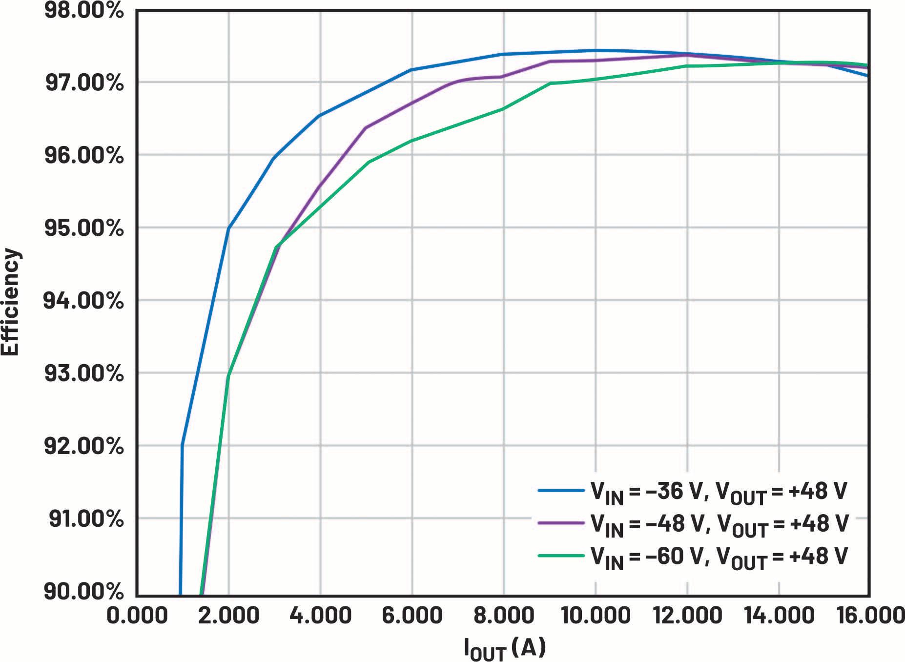
The MAX15258 is a low-frequency boost converter. This reduces the converters' primary source of power loss - switching losses. Because each converter operates in its low-loss area at low frequency, this offers high output power at a high equivalent total frequency. This makes it the go-to device for converting -48VDC Operating with a stable duty cycle, it obtains a high output power with extremely high efficiency. Figure 5 shows the efficiency curves of a coupled inductor-based MAX15258 800W reference design for various combinations of VIN and VOUT. As a result of reduced conduction losses, the plots plainly display efficiency figures more than 98%.
Power supplies play an important role in the telecommunications industry. Due to their ability to attain high efficiency and minimize power losses, active clamp forward converters (ACFCs) are favored in telecom power supply designs. However, inherent limitations can hinder their efficacy in specific circumstances. To overcome the limitations of active clamp forward converters, a new generation of power supply technologies has emerged, offering enhanced efficiency, increased power density, and simplified control mechanisms. In the telecom industry, these novel solutions pave the way for more advanced and optimized power supplies.
Despre autor

Rolf Horn, applications engineer at DigiKey, has been in the European Technical Support group since 2014 with primary responsibility for answering any development and engineering related questions from customers in EMEA, as well as writing and proof-reading German articles and blogs on DigiKey’s TechForum and maker.io platforms. Prior to DigiKey, he worked at several manufacturers in the semiconductor area with focus on embedded FPGA, microcontroller and processor systems for industrial and automotive applications. Rolf holds a degree in electrical and electronics engineering from the University of Applied Sciences in Munich, Bavaria and he started his professional career at a local electronics products distributor as system-solutions architect to share his steadily growing knowledge and expertise as trusted advisor.
DigiKey www.digikey.ro


 Author: Shingo Kojima
Sr Principal Engineer of Embedded Processing Renesas Electronics

Overview
As the working population decreases due to falling birthrates and a growing proportion of the population being elderly, advanced artificial intelligence (AI) processing, such as recognition of the surrounding environment, decision of actions, and motion control, will be required in various aspects of society, including factories, logistics, medical care, service robots operating in the city, and security cameras. Systems will need to handle advanced artificial intelligence (AI) processing in real time in various types of programs. In particular, the system must be embedded within the device to enable a quick response to its constantly changing environment.
This article introduces the RZ/V2H MPU which enables both vision AI and real-time control capabilities. The RZ/V2H is able to respond to the further evolution of AI and the sophisticated requirements of these applications This article introduces how the RZ/V2H solves heat generation challenges, enables high real-time processing speed, and realizes higher performance and lower power consumption for AI-equipped products.
However, AI chips. At the same time consuming less power while performing advanced AI processing in embedded devices with strict limitations on heat generation. To meet these market needs, Renesas developed DRP-AI3 (Dynamically Reconfigurable Processor for AI3) as an AI accelerator for high-speed AI inference processing combining low power and flexibility required by the edge devices. This reconfigurable AI accelerator processor technology, cultivated over many years, is embedded in the RZ/V series of MPUs targeted at AI applications.
RZ/V2H is a new high-end product of the RZ/V series, achieving power efficiency approximately 10 times higher than that of the previous products.
The RZ/V2H is able to respond to the further evolution of AI and the sophisticated requirements of applications such as robots. This article introduces how the RZ/V2H solves heat generation challenges, enables high real-time processing speed, and realizes higher performance and lower power consumption for AI-equipped products.
DRP-AI3
As a typical technology for improving AI processing efficiency, pruning is available to omit calculations that do not significantly affect recognition accuracy. However, it is common that calculations that do not affect recognition accuracy randomly exist in AI models.

This causes a difference between the parallelism of hardware processing and the randomness of pruning, which makes processing inefficient.
To solve this issue, Renesas optimized its unique DRP-based AI accelerator (DRP-AI) for pruning. By analyzing how pruning pattern characteristics and a pruning method are related to recognition accuracy in typical image recognition AI models
(CNN models), we identified the hardware structure of an AI accelerator that can achieve both high recognition accuracy and an efficient pruning rate, and applied it to the DRP-AI3 design. In addition, software was developed to reduce the weight of AI models optimized for this DRP-AI3.
This software converts the random pruning model configuration into highly efficient parallel computing, resulting in higher-speed AI processing. In particular, Renesas' highly flexible pruning support technology (flexible N:M pruning technology), which can dynamically change the number of cycles in response to changes in the local pruning rate in AI models, allows for fine control of the pruning rate according to the power consumption, operating speed, and recognition accuracy required by users.
Heterogeneous Architecture Features in which DRP-AI3, DRP, and CPUs Operate Cooperatively
• Multi-threaded and pipelined processing with AI accelerator(DRP-AI3), DRP, and CPUs
• Low jitter and high speed robot applications with DRP (dynamically reconfigurable wired logic hardware)
Service robots, for example, require advanced AI processing to recognize the surrounding environment. On the other hand, algorithm-based processing that does not use AI is also required for deciding and controlling the robot's behavior. However, current embedded processors (CPUs) lack sufficient resources to perform these various types of processing in real time.
Renesas solved this problem by developing a heterogeneous architecture technology that enables the dynamically reconfigurable processor (DRP), AI accelerator (DRP-AI3), and CPU to work together.
As shown in Figure 1, the dynamically reconfigurable processor (DRP) can execute applications while dynamically switching the circuit connection configuration of the arithmetic units on the chip at each operating clock according to the content to be processed. Since only the necessary arithmetic circuits are used, the DRP consumes less power than with CPU processing and can achieve higher speed. Furthermore, compared to CPUs, where frequent external memory accesses due to cache misses and other causes will degrade performance, the DRP can build the necessary data paths in hardware ahead of time, resulting in less performance degradation and less variation in operating speed (jitter) due to memory accesses.
The DRP also has a dynamic reconfigurable function that switches the circuit connection information each time the algorithm changes, enabling processing with limited hardware resources, even in robotic applications that require processing of multiple algorithms.
The DRP is particularly effective in processing streaming data such as image recognition, where parallelization and pipelining directly improve performance. On the other hand, programs such as robot behavior decision and control require processing while changing conditions and processing details in response to changes in the surrounding environment. CPU software processing may be more suitable for this than hardware processing such as in the DRP.


It is important to distribute processing to the right places and to operate in a coordinated manner. Renesas’ a heterogeneous architecture technology allows the DRP and CPU to work together.
to a maximum of 80 TOPS when compared to models before pruning. This is about 80 times higher than the processing performance of the previous RZ/V products, a significant performance improvement that
In AI-MPUs, a portion of the image processing program is offloaded to the DRP, thereby contributing to the improvement of the overall system processing time. (Figure 4)

An overview of the MPU and AI accelerator (DRP-AI3) architecture is shown in Figure 2. Robotic applications use a sophisticated combination of AI-based image recognition and non-AI decision and control algorithms. Therefore, a configuration with a DRP for AI processing (DRP-AI3) and a DRP for non-AI algorithms will significantly increase the throughput of the robotic application.
RZ/V2H equipped with this technology has achieved a maximum of 8 TOPS (8 trillion sum-of-products operations per second) for the processing performance of the AI accelerator. Furthermore, for AI models that have been pruned, the number of operation cycles can be reduced in proportion to the amount of pruning, thus achieving AI model processing performance equivalent
can sufficiently keep pace with the rapid evolution of AI (Figure 3).
On the one hand, as AI processing speeds up, the processing time for algorithmbased image processing without AI, such as pre- and post-AI processing is becoming a relative bottleneck.
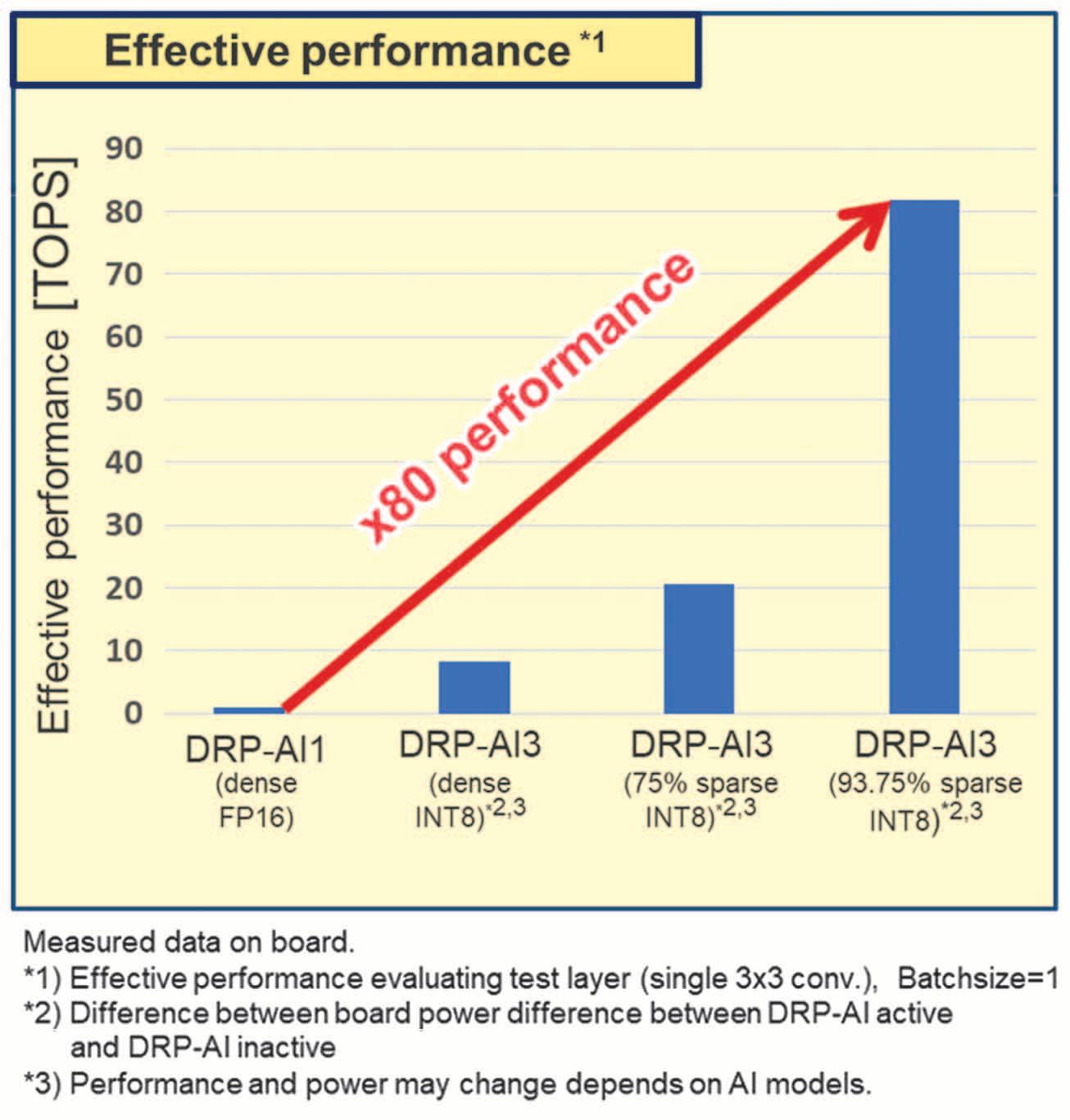
In terms of power efficiency, the performance evaluation of the AI accelerator demonstrated the world's top level power efficiency (approximately 10 TOPS per watt) when running major AI models. (Figure 5)
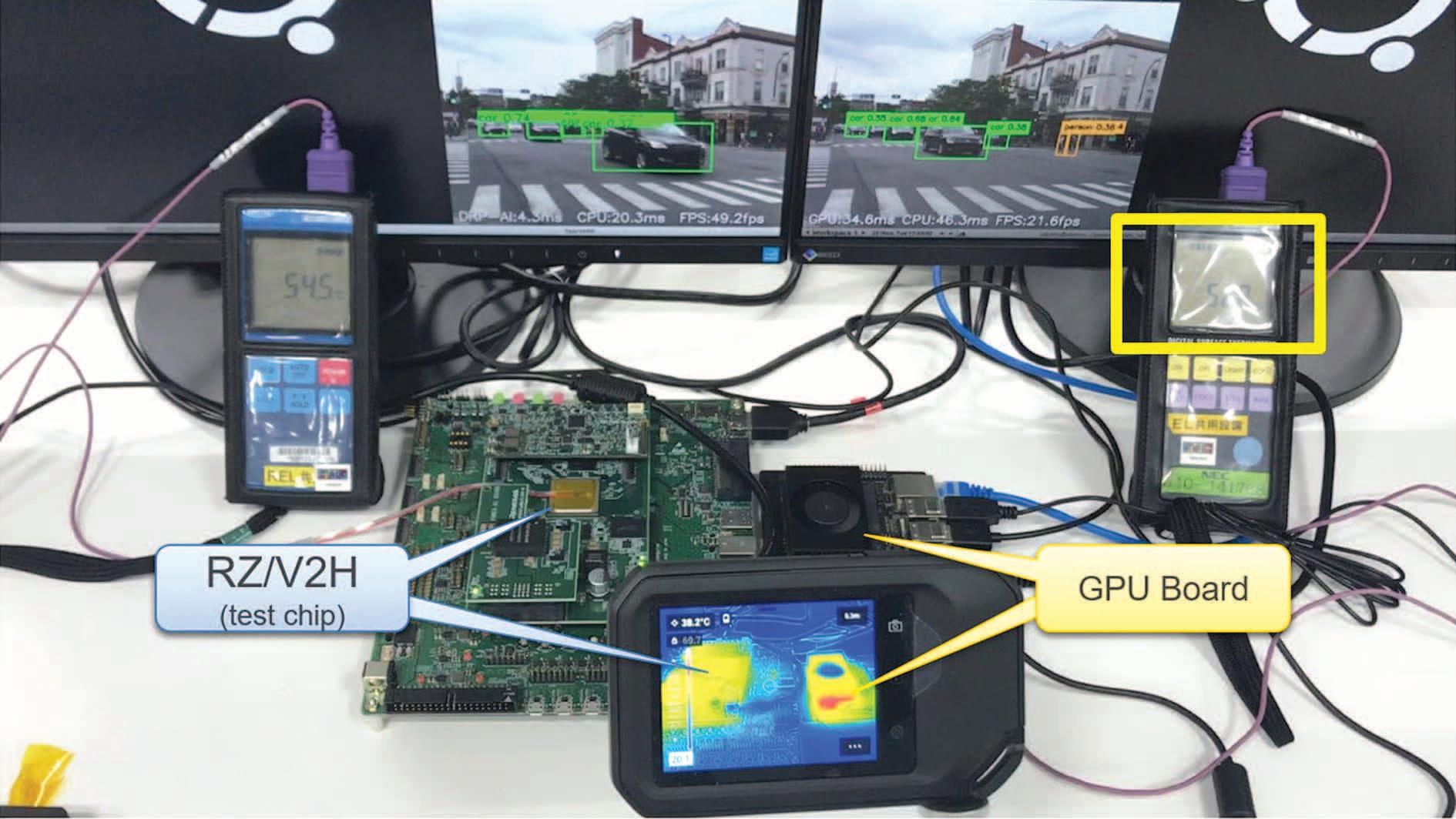
We also showed that the same AI realtime processing could be performed on an evaluation board equipped with the RZ/V2H, without a fan at temperatures comparable to competitor products equipped with fans. (Figure 6)
For example, SLAM (Simultaneously Localization And Mapping), one of the typical robot applications, has a complex configuration that requires multiple program processes for robot position recognition in parallel with environment recognition by AI processing. The Renesas DRP enables the robot to switch programs instantaneously, and parallel operation
with an AI accelerator and CPU has proven to be about 17 times faster than CPU operation alone, and to reduce power consumption to 1/12 the level of CPU operation alone.
Conclusion
Renesas developed RZ/V2H, a unique AI processor that combines the low power and flexibility required by endpoints, with processing capabilities for pruning
AI models, and 10 times more power efficient (10 TOPS/W) than the previous products.
Renesas will release products in a timely manner responding to the AI evolution,

Architecture Speeds Up Image Recognition Processing (Measured by Test Chip).

which is expected to become increasingly sophisticated, and will contribute to deploy systems that respond to end-point products in a smart and real-time manner.
Related Information
• RZ/V2H: https://www.renesas.com/rzv2h
• DRP-AI: Renesas' proprietary AI accelerator that combines high AI inference performance with low power consumption
■ Renesas www.renesas.com


Mouser Electronics, Inc., the New Product Introduction (NPI) leader empowering innovation, has recently released several new eBooks in collaboration with valued manufacturing partner Analog Devices, Inc. (ADI). The eBooks focus on a wide range of topics, such as how production facilities can achieve greater productivity through a flexible manufacturing approach, the technologies being used to support sustainable manufacturing practices, embedded security concepts, and the technological advances in digital factories.
In 10 Experts on Flexible Manufacturing, subject matter experts from ADI and other technology companies discuss how today's sensors, robotic subsystems, and AI-enabled compute units allow factories to adapt fabrication and production with more flexibility. This enables production facilities to achieve greater throughput, product quality and costefficiency than ever before. At the same time, improved processes and control can help facilitate a more sustainable manufacturing process that wastes less energy and materials. The eBook also highlights many of ADI's products that help bring flexible manufacturing to life.
In Engineering a More Sustainable Future: Redefining Industrial Efficiency in the Digital Age, experts from Mouser and ADI explore a wide range of topics related to industrial efficiency. The eBook features more than 10 articles, including a detailed analysis of motor encoders, a single-pair Ethernet condition monitoring vibration sensing solution, and the redesign of an RTD-based temperature sensor for the smart factory age. Several chapters include helpful infographics, as well as links to relevant products from ADI.
Today's embedded devices are expected to measure, store, and communicate data and upgrade firmware securely, but each function represents a system vulnerability point. In Embedded Security: Keeping Edge Data Safe, experts from ADI and other companies take a deep look at embedded security concepts and their importance. ADI has a long history in the field of embedded security and offers customers a broad portfolio of solutions, many of which are highlighted in the eBook.
To learn more about ADI, visit: https://www.mouser.com/manufacturer/analog-devices.
To view more eBooks created by Mouser and ADI, visit: https://analog.mouser.com/adi-ebooks
To browse Mouser's entire manufacturer eBook library, visit: https://resources.mouser.com/manufacturer-ebooks.
■ Mouser Electronics | www.mouser.com

Electronics, Inc., the authorized global distributor with the newest electronic components and industrial automation products, is an authorized global distributor of solutions from MEAN WELL, a leading global standard power supply manufacturer. Mouser offers a comprehensive portfolio of MEAN WELL’s power solutions, with over 4,500 parts in stock and over 35,000 parts available to order.
The MEAN WELL LOP-200 and LOP-300 PCB-type power supplies, available from Mouser, feature a low profile, a comprehensive 12 to 54V voltage range, and power of up to 200 or 300 watts, respectively. The LOP-400, LOP-500, and LOP-600 offer the same voltage range and power of 600, 750 or 900 watts. These power supplies provide compliance with OVCIII and simultaneous adherence to various safety standards such as 62368-1/60601-1/615581/60335-1. These certifications make them suitable for a broad range of applications, including factory automation, medical devices, telecommunications equipment, household devices, and more.
The NGE series are wall-mounted interchangeable AC adapters with global certifications. These green adapters are available with a fixed US plug, a fixed EU plug, or with interchangeable plugs. The NGE series adapters offer power ratings of 12W, 18W, 30W, 45W, 65W, and 90W and are available

with five types of interchangeable AC plugs (European, USA, UK, Australian, and Chinese), making them ideal for travel use. Multiple protections are featured in these adapters, including short circuit, overload, and overvoltage, and all these adapters are approved for ITE, medical, household, and industrial appliance safety regulations.
DDRH-120 and DDRH-240 DIN-rail DC/DC converters offer superior EMC performance, high altitude 5000M operation, and compliance with the IEC/EN 62109-1 PV safety standard. Both converters come with complete protection, including undervoltage and reverse polarity (no damage) for the DC input, as well as short circuit, overload, overvoltage, and overtemperature for the output. These DC-DC converters are suitable for photovoltaic power generation, energy storage, charging stations, industrial control systems, and other applications with high- and low-voltage DC conversion requirements.
The MEAN WELL XLN and XLC series LED power supplies, designed for general indoor lighting and commercial luminaires, feature a rugged plastic housing. These LED power supplies are available in 25W, 40W, and 60W power ratings. The XLN LED power supplies include an independent wiring output design, fully encapsulated to meet IP67 waterproof function. The output and dimming circuits are isolated and comply with double-isolation and safety voltage (SELV) design to ensure user safety. The entire series has complete international certification and full-range voltage input (UIL8750 class 2/class P).
Mouser Electronics has been an authorized distributor of MEAN WELL power solutions since 2007. Mouser received the US Distributor of the Year Award from MEAN WELL for 2023 and a Sustainability Award from the MEAN WELL Sustainable Development Group for 2022.
To learn more about MEAN WELL products available from Mouser, visit www.mouser.com/manufacturer/meanwell
■ Mouser Electronics | www.mouser.com


Compact 10, 30 and 40 Watt railway DC/DC converters with ultra-wide 12:1 input voltage range
The THN 10UIR, TEN 30UIR and TEN 40UIR are railway approved series of high performance DC/DC converters with ultra-wide 12:1 input voltage range and output power of 10, 30 and 40 Watts respectively. The compact, fully encapsulated converters provide an increased resistance against shock/vibration, and thermal shock. A high efficiency of up to 90% give the converters an effective temperature range of –40°C up to +70°C (with heatsink up to 80°C) without derating. Thanks to the dedicated holdup capacitor connection, they meet extended holdup-time requirements without the need for bulky input capacitors. The approvals according to standards EN 50155 and EN 61373 qualify them for railway and transportation systems. Additional qualification for the fire behavior of components according to EN 45545-2 and the safety approval according to IEC/EN/UL 62368-1 support a potential compliance test of the application. All models offer an I/O-isolation voltage of 3’000 VDC and feature an active under voltage lockout function, remote on/off and adjustable outputs to ensure that these converters fit in any ruggedized applications.
• Compact 1″×1″ (THN 10UIR) and 2″×1″ package (TEN 30UIR and TEN 40UIR)
• Ultra-wide input voltage range 9–75, 14–160 VDC
• EN 50155 and EN 61373
• Qualification for fire behavior according to EN 45545-2
• I/O-isolation 3‘000 VDC
• High efficiency up to 90%
• Under voltage lock out circuit
• Adjustable output voltage and Remote On/Off
URL Landingpage: https://www.tracopower.com/thn10uir-ten30uir-ten40uir
URL Video:
https://youtu.be/MnSrBg1LW6Y?si=dc_3w9eb9G140pMT
■ Traco Power | www.tracopower.com
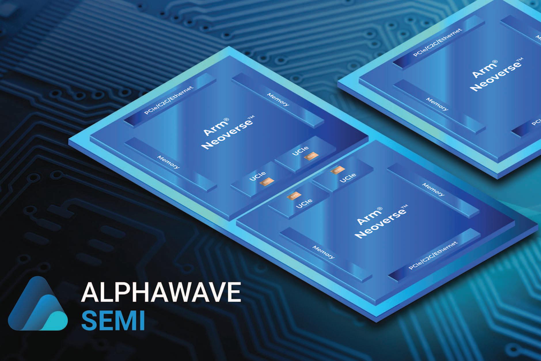
Arm Neoverse CSS-based CPU chiplet with ultrahigh-speed interfaces and advanced packaging delivers scalable performance for AI, HPC and networking infrastructure
Alphawave Semi, a global leader in high-speed connectivity and compute silicon for the world’s technology infrastructure, has collaborated with Arm on the development of an advanced compute chiplet built on Arm® Neoverse™ Compute Subsystems (CSS) for artificial intelligence/machine learning (AI/ML), high-performance compute (HPC), data centre and 5G/6G networking infrastructure applications. The development follows last year’s announcement that Alphawave Semi joined Arm Total Design, an ecosystem building custom silicon solutions based on Arm Neoverse CSS.
Alphawave Semi’s chiplet-based custom silicon design platform adds a differentiator in our portfolio that includes IO extension chiplets, memory chiplets, and compute chiplets, as well as Alphawave Semi’s ultra-high-speed connectivity IP and advanced packaging capabilities. This compute chiplet lineup features an Arm Neoverse N3 CPU core cluster and the Arm Coherent Mesh Network (CMN) ensuring efficient, scalable performance. Available on industry-leading process nodes, the technology allows customers to accelerate development and reduce the time-to-market (TTM) of a new generation of custom system-on-chip (SoC) technologies. These advanced SoCs support the rapid deployment of high-performance digital infrastructure, enabling the creation of custom silicon solutions tailored to specific needs.
In collaboration with Arm, Alphawave Semi enhances this setup with their advanced packaging techniques and a leading-edge portfolio of connectivity technologies, including PCIe Gen 6.0 and 7.0, Universal Chiplet Express (UCIe), 112/224G Ethernet and HBM subsystems. This strategic integration ensures that the Arm-based compute chiplet delivers robust performance and flexibility, catering to next-generation HPC, data center, AI/ML, and 5G/6G infrastructure needs while accelerating time-to-market for customers.
■ Alphawave Semi | https://awavesemi.com
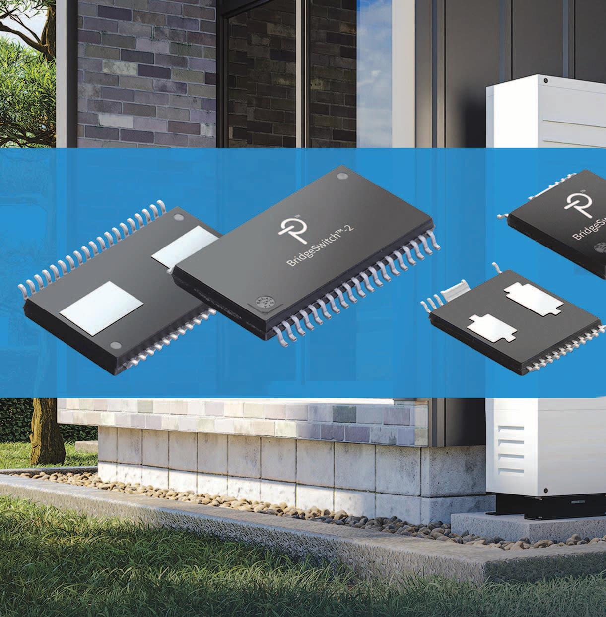
Power Integrations, the leader in high-voltage integrated circuits for energy-efficient power conversion, today enhanced its hardware-software bundle for brushless DC motors (BLDC) with BridgeSwitch™-2, a new high-voltage integrated half-bridge (IHB) motor-driver IC family targeting applications up to 1 HP (746 W). The new ICs, which feature high- and low-side drivers and advanced FREDFETs with integrated lossless current sensing, deliver inverter efficiency of up to 99 percent. The IHB architecture eliminates hot spots, which increases design flexibility and reliability, slashes component count and saves PCB area. BridgeSwitch-2 is supported by Power Integrations’ MotorXpert™ software suite which includes single-phase trapezoidal control and three-phase sensor-less Field Oriented Control (FOC) modules, speeding inverter development.
BridgeSwitch-2 ICs handle operational exceptions in hardware, which permits the use of IEC 60730 Class A safety software, reducing certification time by months. Quiescent BLDC inverters can be ordered into sleep-mode, reducing driver power consumption to less than 10 mW; this leaves more power available under regulated standby power limits to be allocated for loads such as network access and monitoring.
Cristian Ionescu-Catrina, product marketing manager at Power Integrations, said: “The low standby consumption of BridgeSwitch-2-based motor drives enables designers to meet new and emerging EU ERP regulations. BridgeSwitch-2 ICs are also far more efficient than IGBT based IPMs across the entire load range.” He continued: “From startup to perform-

BLDC motor hardware-software combo slashes inverter sleep-mode consumption to less than 10 mW, expands output power to 1 HP
ance optimization, the GUI-based tool, terminal emulator and MISRA C-compliant code library of MotorXpert greatly simplifies the design process, allowing the motor architecture to be optimized in real-time without repeated firmware updates.
BridgeSwitch-2 is microprocessor agnostic, easing its adoption into existing systems – this is important as engineers update designs to meet more stringent standby regulations.”
BridgeSwitch-2 ICs address a power range of 30 to 746 W (1 HP), encompassing a broad range of applications including heat exchanger fans, refrigerator compressors, fluid and circulation pumps, gas boiler combustion fans, washing machine drums and kitchen blenders and mixers. The IHB architecture reduces component count by 50 percent and PCB space by 30 percent over discrete designs by eliminating shunt resistors and associated signal conditioning circuits. Shunt losses are also eliminated, improving efficiency. Precise motor control is achieved with the built-in real-time reporting of phase current (IPH) information. Accurate turn-on/off gate drive and a soft-body diode result in a typical EMI profile 10 dB lower than existing drivers, so a smaller EMI filter can be selected.
BridgeSwitch-2 ICs feature built-in DC overvoltage protection and current limits that protect the inverter and the system without relying on system software. The choice of error-flag or comprehensive fault bus reporting supports a range of system requirements. Emerging use-cases like failure prediction are now possible with the high accuracy of the built-in IPH information and comprehensive reporting via the fault bus.
BridgeSwitch-2 motor drives use built-in, hardware-based lowand high-side over-current protection to meet IEC 60335-1 Class A requirements. BridgeSwitch-2 also works without an auxiliary power supply, further reducing PCB area and component count.
■ Power Integrations | www.power.com


Packages with enhanced thermal performance improve power density and reliability, while power modules with a wide range of topology options simplify and accelerate high-performance design.
WeEn Semiconductors, has unveiled new families of silicon carbide (SiC) MOSFETs and Schottky Barrier Diodes (SBDs) in TSPAK packaging at this year’s PCIM Europe exhibition and conference.
WeEn Semiconductor’s new TSPAK MOSFET and SBD devices address the demand for high-performance, compact and reliable power management in applications ranging from automotive charging and on-board charger applications to photovoltaic (PV) inverters and high-power-density power supplies (PSUs).
Offering a variety of configuration options for maximum design flexibility, the company’s new SiC modules are ideal for applications such as EV charging, energy storage systems, PV inverters, motor drives, industrial PSUs and test instrumentation.
Originally developed for automotive applications, TSPAK devices combine innovative top-side cooling capability with low thermal impedance to deliver enhanced thermal performance. By removing the PCB thermal resistance from the thermal dissipating path, the Junction-Ambient thermal resistance improves by 16-19%. This supports high reliability by enabling a greater number of power cycles than conventional packaging as well as providing the increased power densities demanded by compact system designs. Low circuit inductance and low EMC noise help to improve performance and reduce filtering requirements. The WeEn Semiconductors family of TSPAK MOSFETs features 650V, 750V, and 1200V options with resistances ranging from 12mΩ to 150mΩ. TSPAK SBDs are available with current ratings of 10 to 40A in 650V, 750V, and 1200V variants.
For more information, please explore WeEn Semiconductors’ product portfolio here.
■ WeEn Semiconductors | www.ween-semi.com/en

 Author: Edgar Schäfer, Field Application Engineer Automotive Business Unit (ABU) Rutronik

Among the biggest challenges facing electric vehicle users are battery life and range. One way to increase both is to improve the efficiency of the entire vehicle. However, there are major consumers in the car standing in the way. One of them is the air conditioning system. The electric powertrain has less power loss than an internal combustion engine and therefore has less waste heat that can be used to heat the interior. This means that in electric vehicles, additional electric heating is required to achieve or maintain the desired temperature.
Ways to create an efficient air conditioning system
One way to increase the efficiency of the air conditioning system is to reuse the air in the interior (recirculation). In the winter, heated air is reheated, while in the summer, conditioned air is recooled and fed back into the interior. Since only a smaller temperature difference needs to be bridged, less energy is required.
How CO2 sensors in electric vehicles help maintain healthy air quality inside the vehicle while extending battery life and range.
A major disadvantage of this method is that no fresh air is supplied to the interior. If the used air is not renewed, CO2 levels increase and the air quality inside
the vehicle gradually deteriorates. This may result in headaches, fatigue, and a less-than-ideal driving experience.
This represents a potential source of danger in road traffic, as ventilation measures are necessary above CO2 levels of 1000 ppm.
One solution is to use CO2 sensors for control purposes. When integrated into the vehicle’s air conditioning system, they monitor the air quality inside the vehicle. If CO2 values are too high, a warning can be output or fresh air can be added directly to maintain healthy air quality.
Choosing the appropriate sensor for electric vehicle applications depends on several factors. These include the size of the vehicle, the desired measurement range, and the type of measurement.
Furthermore, the dimensions, performance, and cost of the sensors are crucial.
Small and precise CO2 sensor
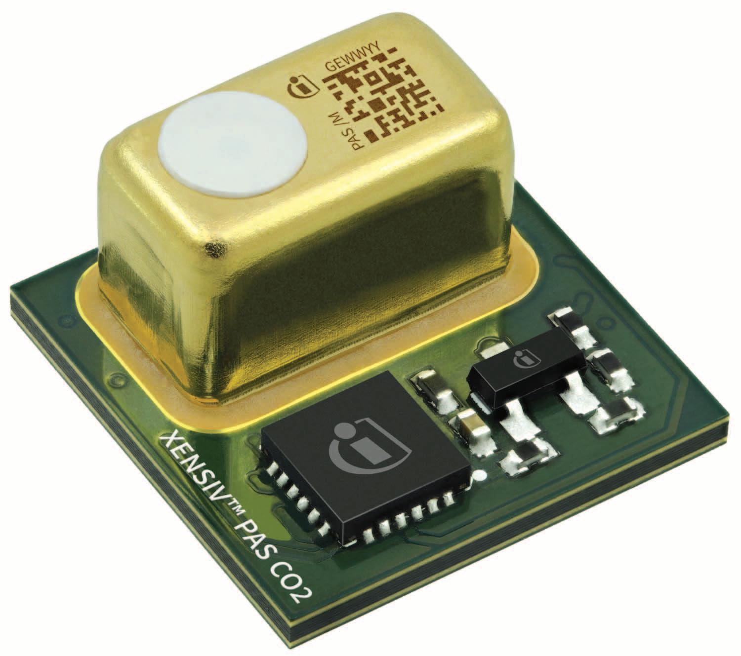
A CO2 sensor with a particularly small form factor (14 mm × 13.8 mm × 7.5 mm) is the Xensiv PAS from Infineon (Figure 1). It reduces the space requirement by more than 75 percent compared to commercially available CO2 sensors.
At the same time, it offers precise CO2 measurements based on MEMS technology. For example, on a printed circuit board the Xensiv PAS CO2 sensor integrates a photoacoustic converter, including a detector, an infrared source and an optical
filter, a microcontroller for signal processing and algorithms, and a MOSFET chip to drive the infrared source. The integrated microcontroller performs ppm calculations as well as advanced compensation and configuration algorithms. The result is the true CO2 content and not just a correlation. In addition, various configuration options (e.g. measurement frequency, baseline calibration) and interfaces (UART, I2C, PWM interface) are available. The spectrum for the CO2 measurement covers a range from 0 ppm to 32,000 ppm. The accuracy is ±30 ppm ±3 percent of the read measured value. The supplier guarantees it for the measurement range of 400 to 5000 ppm, which is perfectly adequate for this range of applications. This is because a typical atmosphere has a CO2 content of 400 ppm; the value inside the vehicle is typically higher.
Further advantages for customers are to be found in the production process. Infineon claims to offer the first SMD-capable CO2 sensor (SMD package, available on tape & reel) to comply with the international JEDEC standard for lead-free surface-mount reflow – for easy assembly as well as system integration even at high production volumes. The Xensiv PAS CO2 sensor also offers a high degree of flexibility thanks to a wide range of configuration options, enabling a fast time to market.
The PAS method is based on the photoacoustic effect: Gas molecules absorb light of a certain wavelength, causing them to expand. In the case of carbon dioxide, it is the 4.2 μm wavelength.
Light pulses are emitted in rapid succession by an infrared source. Only light with a 4.2 μm wavelength enters the sensor chamber via an optical filter that is specially adapted to CO2 molecules. The CO2 molecules in the sensor chamber absorb the energy.
Rapid heating and cooling causes thermal expansion and contraction. This produces a change in pressure, which is detected by the highly sensitive
An evaluation kit consisting of the Xensiv PAS and a microcontroller of the PSoC4100S family for data evaluation are also available.

PSoC 4100S Max microcontroller for data evaluation.
The features and capabilities of the Xensiv PAS make the sensor the ideal choice for intelligent control of air conditioning systems in e-cars. On the one hand, it ensures optimum air quality, contributing to passenger safety. On the other hand, it increases efficiency for improved battery life and range.
■ Rutronik www.rutronik.com

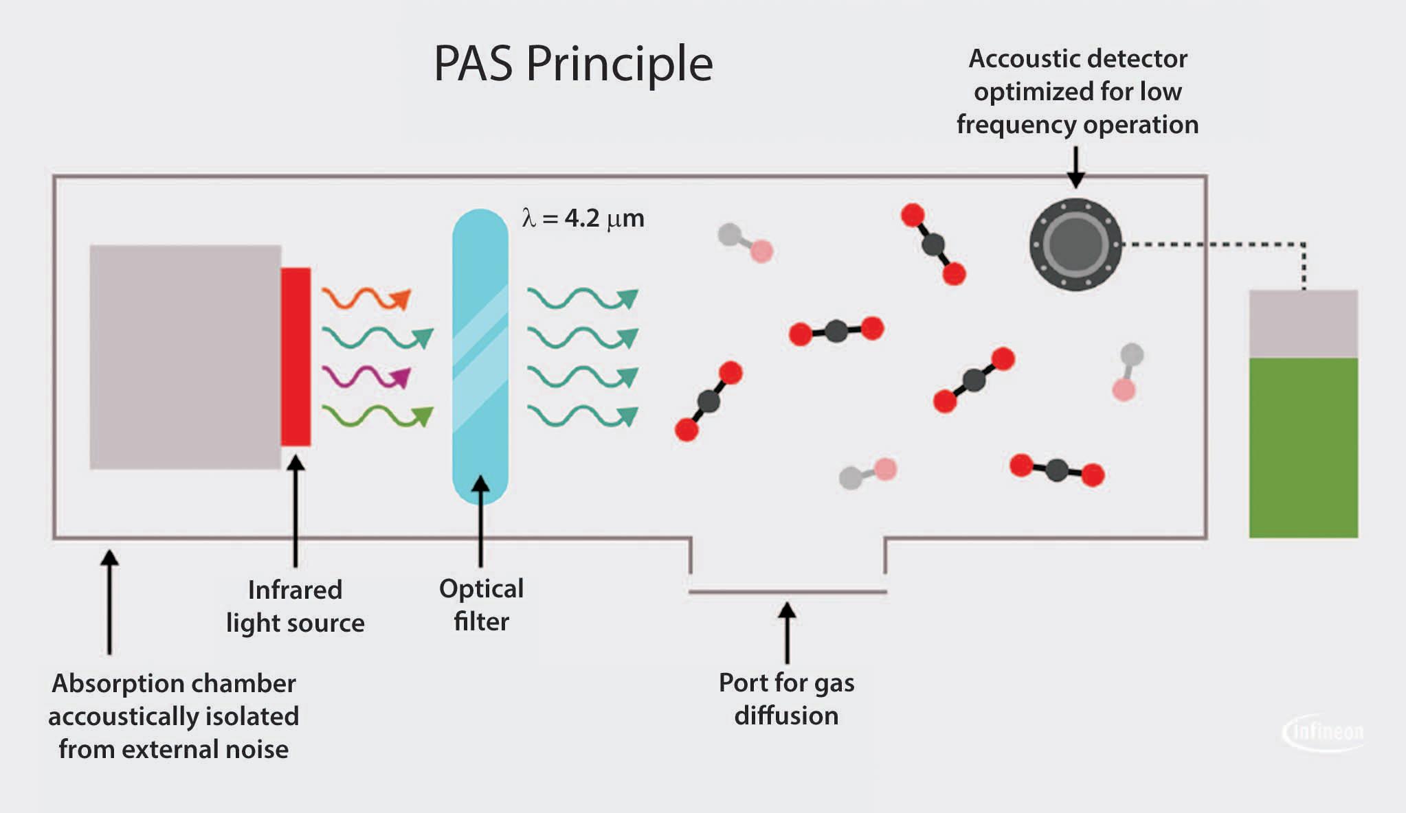
MEMS detector. The higher the CO2 concentration in the chamber, the stronger the signal. The signal is processed by an integrated microcontroller, which outputs the result in real time as ppm (parts per million). For the most accurate results, the acoustic detector is optimized for low frequencies and the absorption chamber is acoustically shielded from external noises.


What does the 2024 distribution market look like so far?
DigiKey’s vice president of global business development, Mike Slater , offers engineers and designers a mid-year look at the market

We expect to see signs of further design activity, with more new product introductions and projects coming to fruition toward the end of Q2. Hopefully, by the end of the year, we will see reasonably increased demand for electronic components as technology evolves.
Many key vertical markets in Europe will develop further in 2024, including renewable energy, electric vehicles, cellular networks, IoT and artificial intelligence (AI).
What distinguishes your market action in Europe?
DigiKey continues to invest in our infrastructure, systems and inventory to support all our European customers over the next few exciting years in our industry. Our purpose in EMEA is to accelerate progress for engineers, designers and buyers while making interactions with DigiKey easy and efficient.
We offer our European customers the world’s largest selection of electronic components in stock and available for immediate shipment, and we can get products
into the hands of customers in Europe in as little as 48 hours.
What new products and partnerships are you focusing on today? How do you choose a new supplier?
DigiKey wants to seed the Romanian market with the latest new product introductions from European suppliers. DigiKey has certain supplier criteria and requirements, including product quality, brand authorization, compliance with industry standards, reliability, liability insurance and the ability to meet customer demands.

What services can your customers rely on? How is your service offering evolving? Beyond the products that accelerate technology innovation, DigiKey also supports engineers with a wealth of digital solutions and tools to make their jobs more efficient.
We publish hundreds of articles, blogs, webinars and videos on our website, https://www.digikey.com and we have other digital assets, such as our TechForum for problem-solving and Maker.io site for projects and ideas.
We have also launched an “Innovation Hub” as a web immersive experience to help introduce engineers and designers to DigiKey and our products and services. We also recently launched a new webpage dedicated to the Industrial Sector, which focuses on solutions for robotic arms, AGVs and conveyor belts. DigiKey continues to invest in more robust and predictive web search functionality, higher inventory levels and increased automation in the DigiKey warehouse, which all benefit customers by providing an easy and efficient research, shopping and delivery experience.


What technology scenarios are you ready to bet on for the future? Where do you see the greatest room for growth?
Wireless connectivity, industrial automation and electrification, smart sensors, cross-architecture solutions and rapid prototyping are all key technology trends this year. The most talked about trends recently are related to AI and data. Many companies are starting to scratch the surface and try things that have the potential to significantly change the way we do business long term. We’re excited to help engineers, designers and makers accelerate progress in these spaces.
In Europe, we continue to see clean automation and control, energy, automotive and transportation, electrification, and aerospace perform well. In the long term, we are very optimistic that the electronics business and industry will continue to proliferate in areas we have not seen in the past.
What is your business strategy in Europe going forward?
We want to emphasize how important Romania and the European region are to DigiKey. This area always drives innovation and demand. We are laser-focused on superior execution and customer experience for our European customers in 2024.
Last year, we added considerable inventory depth to offer the industry the widest product availability for immediate shipment and are thrilled with the customer response. We closed Q4 2023 seeing more than 10% in new customers compared to Q4 2022.
The customer growth we experienced at the end of 2023 corresponds directly with increases in new design activity we saw earlier in the year and is a positive sign for DigiKey’s and the overall industry’s future.
What business goals have you set for 2024?
In 2024, we plan to build upon our foundation of high-performing teams, strong digital strategy and superior operational excellence, which will together drive our growth in inventory, eCommerce, supplier services, and new markets and geographies.
With those strategies in place, we expect to grow our revenue and annual customer count, expand our market share, and become increasingly scalable.
All those advancements benefit our European customers and future customers, and we look forward to exceeding their expectations in 2024 and beyond.
■ DigiKey www.digikey.com


 Author: Sundara Venkatesh Market Development Anritsu Corporation
Currently, operators are focusing on Open Radio Access Network (Open RAN), as it promises a more cost-effective and agile RAN that can be used for 4G, 5G and beyond 5G networks.
Designed around the use of open interfaces, commercial off-the-shelf (COTS) hardware, and possibly open-source software, Open RAN offers a number of benefits. Among these is lower costs. CAPEX can be reduced thanks to the economies of scale provided by a multi-vendor ecosystem, while OPEX is also lowered because of the use of learning-based technologies to power RAN automation.
Lower RAN costs allow mobile operators to serve more cost-sensitive 5G network use cases, for example, rural markets or private 5G networks. Open RAN can also use APIs that readily plug into open systems developed by new entrants to the market.
Open RAN offers improved efficiency and performance thanks to better management of radio resources achieved through real-time and non-real-time RAN Intelligent Controllers (RICs).
Mobile network operators are constantly looking for ways to improve the network experience for their subscribers, while at the same time making their networks more efficient, capable and cost-effective.

Expanding network capability is also simplified because of Open RAN’s cloudnative infrastructure and the use of Agile Continuous Integration, Continuous Test, and Continuous Deployment methods (CI/CT/CD).
BUILDING BLOCKS OF OPEN RAN
Open RAN can be deployed using either LTE or 5G, and splits traditional base station hardware and software into OpenCentralized Unit (O-CU), Open-Distributed Unit (O-DU), and Open-Radio Unit (O-RU), all with open interfaces. Engineers need to understand the implications of such a split, particularly at the O-RU and O-DU layers connected via the Open Fronthaul Interface (O-FH). For example, radio in a traditional base station is typically sent over-the-air (OTA). With Open RAN, it travels first as IQ data over the O-FH before it is sent OTA.
Intelligent radio controllers unleash the potential of a fully automated network.
The architecture proposed by the O-RAN ALLIANCE (O-RAN) uses COTS hardware
and virtualized software to provide numerous hierarchical cloud deployment options for operators. Open RAN provides the cloud framework to help operators automate the deployment and provisioning of O-RAN based radio access networks.
The O-RAN architecture consists of Virtualized Network Functions (VNFs) and/or Physical Network Functions (PNFs). Also included is a Service Management and Orchestration (SMO) framework to manage the network functions.
Formed by some of the leading global operators, the O-RAN ALLIANCE defines open standards and interfaces for interoperability between O-RU, O-DU, and OCU. The O-RAN ALLIANCE has test labs known as Open Testing and Integration Centers (OTICs). A number of test and measurement vendors participate in events held at these centres to help develop test solutions for Open RAN verification and deployment.

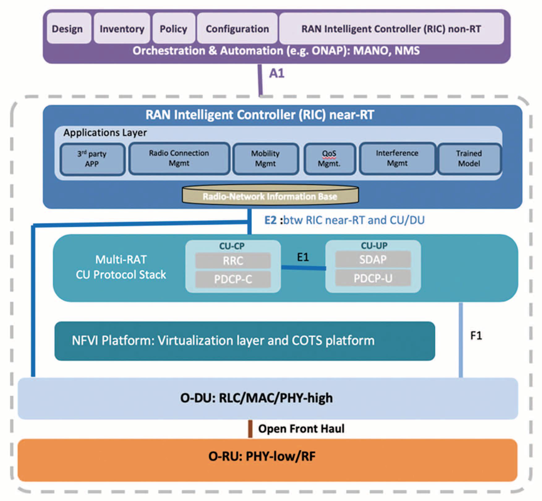
The O-RAN ALLIANCE provides procedures for certifying and badging vendor equipment - these ensure equipment conformance, interoperability, and performance based on specifications. Certification is applied using conformance tests to confirm that an individual device-under-test (DUT) meets the O-RAN technical specification. Two badges - interoperability tests (IOT) and end-to-end (E2E) tests – can be acquired. These involve multiple DUTs from different vendors. IOT assesses the interoperability of DUT pairs using O-RAN Interoperability Test specifications.
E2E system integration badging is defined as an assessment of end-to-end system integration of DUT groups that are implemented according to O-RAN interfaces using O-RAN E2E test specifications.
E2E test requirements and methods are similar to a monolithic base station but with additional test sequences that include the O-FH verification – the RF interface verification is the same as the 3GPP BTS test specifications.
“Wrap-around” test setup for O-RU and ODU as Subsystem Pair under Test
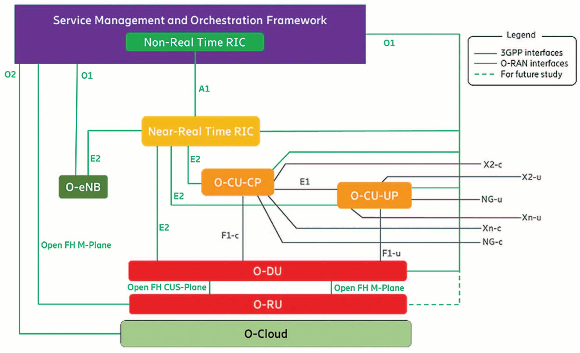


Emulated network functions include a UE simulator for functional/load tests, ensuring a framework for comprehensive evaluation and testing before the start of E2E system testing.
“Wrap-around” testing is used to verify the O-RU and O-DU and involves emulating or using reference test platforms for the relevant subsystems to create real-world environments as defined in the O-RAN Deployment Blueprint. Reference test platforms can be subsystems designed for commercial purposes or test applications, which are used to support the wraparound test setup. The reference test platform, or test application, should be capable of “full speed” online operation to measure KPIs. An offline test tool can conduct O-RU conformance tests but not interoperability and E2E KPI tests.
To implement Open RAN successfully, a comprehensive testing strategy must be developed.
This poses challenges due to the open environment and the multitude of players that vary in size and experience. At a minimum, Open RAN elements and networks must meet the performance of 5G monolithic systems.
Test solution providers who are active members of the O-RAN ALLIANCE can gain a greater understanding of specifications, open software development, testing needs, and integration.
Among the tests that must be conducted are:
• RU RF Performance Test – Follows 3GPP requirements to verify RF parametric values of RU radio elements.
• O-FH Conformance Test – Verifies O-RU conformance to O-FH interface and related performance of O-RU.
• O-FH Interoperability Test – Verifies interoperability between different O-RU and O-DU suppliers/implementations.
• End-to-End System Testing – Assures sub-system and E2E performance against KPIs.
• Open X-Haul Transport Network Testing (Real World I&M test) – Assures Transport Network requirements.
Figure 4 outlines a configuration to test O-RAN fronthaul conformance. The O-RU is connected to Test Equipment O-RU (TER), which surrounds the DUT and connects to the fronthaul interface and radio interface to make measurements.
The TER has three main components - a CUSM-Plane Emulator (CUSM-E), a signal analyzer, and a signal generator to perform RF measurements. The TER collects RF signals from the DUT (Downlink: DL) and sends RF signals to the DUT receiver (Uplink: UL) at the radio interface. The DL data flow is evaluated based on what is received by the signal analyzer in the RF domain as radiated by the O-RU. The UL data flow is evaluated based on what is emitted by the signal generator in the RF domain as received by the CUSM-E.

When conducting tests, engineers must be aware of considerations specific to the Open RAN ecosystem.
Among these are:
• Wide range of DU+RU combinations leads to numerous test cases.
• Multi-vendor RAN is new to many vendors and operator test engineers.
• Partnering with third-party integrators is beneficial to target E2E test solution based on key players in question.
• Conformance, compliance, and interoperability certifications needed in supply chain.
• Capacity, performance, and compliance testing with emulation of Open RAN nodes, interfaces, and RF channels support key deployment KPIs.
• Difficulty of reproducing field synchronization, latency and performance issues in the lab
• Multiple use cases may require specific measurements/testing.
• Require test solutions that integrate Open RAN to existing brownfield implementation.
Open RAN architecture is used across different vertical industries, with different levels of customization. Combined with a large number of new companies entering the market, we need to ensure elements work together seamlessly. Automated testing is required to reduce complexity, as well as control test costs and cut time-to-market. Test solutions that are completely integrated with standards and can perform the tests in a few keystrokes offer the required accuracy, repeatability, and speed.
Flexible platforms that support updates as specifications evolve are also beneficial for Open RAN.
Also useful are software-based solutions that automatically update 3GPP test cases in test tools, saving time and money for production test environments. The Open RAN architecture can create an open environment that adds flexibility, intelligence, and cost efficiency to 4G and 5G networks and aims to help build smarter, innovative, and cost-effective mobile infrastructure. Ensuring that Open RAN is widely adopted demands sound testing to assure Open RAN compatibility and network security.
■ Anritsu Corporation www.anritsu.com



Accessory device to Microchip’s TimeProvider 4100 grandmaster scales up to 200 fully redundant T1, E1 or CC synchronization outputs
Critical infrastructure communication networks require highly accurate and resilient synchronization and timing, but over time these systems age out and must be migrated to a more modern architecture. Microchip Technology today announces the new TimeProvider® XT Extension System, a fan-out shelf used with redundant TimeProvider 4100 grandmasters to migrate legacy BITS/SSU equipment to a modular and resilient architecture.
The TimeProvider XT provides operators with a clear path to replace existing SONET/SDH frequency synchronization equipment while adding timing and phase, essential for 5G networks.
As an accessory device to Microchip’s widely deployed TimeProvider 4100 grandmaster, each TimeProvider XT shelf is configured with two distribution modules and two plug-in modules to provide 40 fully redundant and individually programmable outputs with synchronization designed to meet ITU-T G.823 for wander and jitter control. Operators can connect up to five XT shelves to scale up to 200 fully redundant T1/E1/CC communication outputs. All configuration, status monitoring and alarm reporting is done via the TimeProvider 4100 grandmaster.


This new solution allows operators to consolidate their critical frequency, timing and phase requirements onto a single modern platform, saving maintenance and service costs.
“With the new TimeProvider XT Extension, network operators can take advantage of state-of-the-art technology that is reliable, scalable and flexible to either overlay or replace their SONET/SDH synchronization systems,” said Randy Brudzinski, vice president of Microchip’s frequency and time systems business unit. “The XT solution is an attractive investment for network operators because it is more than just a replacement for legacy BITS/SSU equipment; it also adds PRTC functionality, delivering frequency, time and phase for nextgeneration networks.”
This solution is compatible with DCD, SSU 2000, TSG-3800 and TimeHub® systems’ wire-wrap and output panels, so that network elements do not have to be rewired. This can save network operators significant deployment time and resources while reducing costs.
The TimeProvider XT has a Composite Clock (CC) input which allows for live inservice CC phase cutovers, which are typically performed during maintenance


windows to ensure that the synchronization in a network is maintained. The TimeProvider XT system requires the TimeProvider 4100 grandmaster to be running the latest version 2.4 firmware.
The TimeProvider XT Extension system is the newest product to join Microchip’s extensive portfolio of clock and timing systems, which ranges from small plug-in timing server cards to multi-rack national and time scale systems. As a primary contributor to the world’s time, Microchip’s timing solutions are trusted, reliable and resilient.
For more information, visit Microchip’s Timing and Synchronization website
Development Tools
The TimeProvider XT Extension is supported by TimePictra® Management Software, a web-based tool to manage and monitor synchronization architectures.
Pricing and Availability
The TimeProvider XT Exension is now available for purchase. For additional information and to purchase, contact a Microchip sales representative or an authorized distributor.
Microchip Technology www.microchip.com

 Author: Frederik Dostal, Power Management Expert Analog Devices
QUESTION
The Intelligent Edge is spreading across the industry, replacing heritage edge sensors and actuators. Can the Intelligent Edge use common heritage power supplies?
ANSWER
In some cases, yes, but in most cases, no! Adapted, more advanced power supplies need to be designed.
INTRODUCTION
The field of power supplies for industrial sensors is currently ripe with innovations and rife with challenges. Implementation of an Intelligent Edge requires intelligent data preparation. This requires innovations in power supplies. In some cases, sensors at the Intelligent Edge need to be powered

by a single twisted pair cable, which a single-pair power over Ethernet (SPoE) solution can provide. In other applications, a nanopower solution helps to save energy to achieve longer run times with a battery at the sensor side.
Furthermore, some intelligent sensors require an ultralow noise power supply, so that sensor data is not compromised. Finally, adding sensor intelligence at the edge will require a power supply with a higher power density. This is because new sensors need to fit in an existing form factor.
WHAT IS THE INTELLIGENT
The term Intelligent Edge refers to sensors in industrial systems that can select and process data independently.
This article introduces different examples of the implementation of Intelligent Edge sensors and how power management solutions are selected and adapted to provide the best solution. This article will explore some of these sensor solutions available today.
A lower volume of data is transmitted between the sensors and the central control unit, so data transmission is less challenging. Of course, a microcontroller is needed to process the data supplied by the sensors. A simple example is an optical sensor used for the detection of specific information.
For example, it may detect people who accidentally step into an automated manufacturing area, thereby putting themselves in danger. The image data must be processed in such a way that a person can be unequivocally identified so that the machines can be shut down quickly in response. This should serve to prevent injuries. The goal is to have the image data processed at the Intelligent Edge.
Only one signal, which is the person detected in the camera’s field of view, is transmitted to the central computer. Transfer of image data to the central computer is done away with. As a result, less transmission bandwidth is required and transmission is simplified.
Through the additional processing unit (microcontroller) at the Intelligent Edge, a smart sensor is created. However, this unit has a higher current consumption. New concepts for supplying the higher current needed at the sensor are required. This is especially true for existing industrial plants and infrastructure.
The solutions should provide easy and secure means of meeting the higher current needs, in addition to enabling secure data transmission.
OF THE INTELLIGENT EDGE WITH AN EXISTING 2-WIRE CABLE (A 4 mA TO 20 mA INTERFACE, FOR EXAMPLE)
SPoE helps realize the Intelligent Edge since it can be used as a power supply via a 2-wire cable. SPoE is similar to power over Ethernet (PoE), but it can be implemented with an existing 2-wire cable (such as a 4 mA to 20 mA interface). With SPoE, up to 52 W can be transmitted over 400 meters or up to 20 W over a distance of up to 1 kilometer. SPoE is specified in the IEEE 802.3cg standard.
The line is operated at a voltage of 24 V or 55 V. The special feature of this type of power supply is that both energy transmission and data transmission can take place on the same 2-wire cable.
Data communication is based on the 10BASE-T1L standard. Figure 1 shows an SPoE for supplying up to 52 W via a single 2-wire cable up to 1 km in length.
An example of a low power sensor in an industrial environment in the context of the Intelligent Edge is vibration sensors distributed in a process plant to monitor individual machines.
The recorded vibrations correspond to different frequencies and provide an indication of whether mechanical bearings and shafts can still be operated reliably. Early signs of aging can be identified from them. Through this, the probability of unplanned asset downtime or operation outside specific tolerances can be lowered. Such a reaction is made possible through the precise measurement of the vibrations. Monitoring of vibration data requires sophisticated algorithms that evaluate large amounts of data in real time. The data processing can take place locally at the location of deployment or a central location. With centralized evaluation, all the sensor data gathered must be transmitted either by cable or wirelessly by radio waves.
In many applications, it is advantageous to implement data evaluation locally, right at the sensor. For such an implementation, existing industrial plants can simply be equipped with vibration sensors; no additional cables have to be laid. A sensor then just delivers a defined warning signal if it detects a frequency range outside the tolerances. This type of sensor can be magnetically fastened to a machine or piece of equipment and delivers data via radio waves, often in a mesh network.
In such a mesh network, various sensors communicate with one another and transmit information about which bearing is showing pronounced signs of aging. An industrial plant can thus easily be equipped with predictive maintenance capabilities. One example of this is the Analog Devices OtoSense™ Smart Motor Sensor (SMS) technology. It is an AI-based turnkey hardware and software solution for condition-based monitoring. The ADI OtoSense SMS monitors the condition of electric motors by combining best-in-class sensing technologies with leading-edge data analysis.
An important prerequisite for a functioning system is the availability of a suitable energy supply for the sensors. The vibration sensor must provide the appropriate power supply not just for the sensor itself but also for the operation of the local microprocessor for evaluation of the data as well as the RF modules used for wireless communication. The sensor system is designed for minimal current consumption. A battery can be in place as an energy source, or energy harvesting can be used. The two technologies are often utilized together. Energy harvesting is added to extend battery life. As a result, the battery does not have to be replaced as frequently. Various energy sources are possible for energy harvesting. Depending on the sensor location, solar cells, thermoelectric generators (TEGs), or piezoelectric converters can be used. Especially in industrial process plants, there are often temperature gradients that can be converted into electrical energy with TEGs. Mechanical movements can also be converted into electrical energy with the help of piezoelectric sensors.


For devices powered by batteries and by energy harvesting alike, optimal voltage conversion plays a key role. High efficiency is essential. Several different nanopower management integrated circuits exist for this.
Figure 2 shows an example of a voltage conversion circuit with the MAX38650. It is a 100 mA nanopower step-down switching regulator. It can be operated with up to 5.5 V supply voltage on the input side and can supply a regulated output voltage of between 1.2 V and 5 V. During operation, the switching regulator only draws 390 nA of current itself (typical value). This is a very low quiescent current.
A resultant voltage sets the required output voltage for the entire operating duration of the voltage converter. This is the best of both worlds: a low leakage current during operation and an adjustable, robust output voltage.
Many sensors can measure extremely small signals. A very low noise power supply must be used to prevent these signals from being distorted. Conducted and radiated interference sources play major roles.
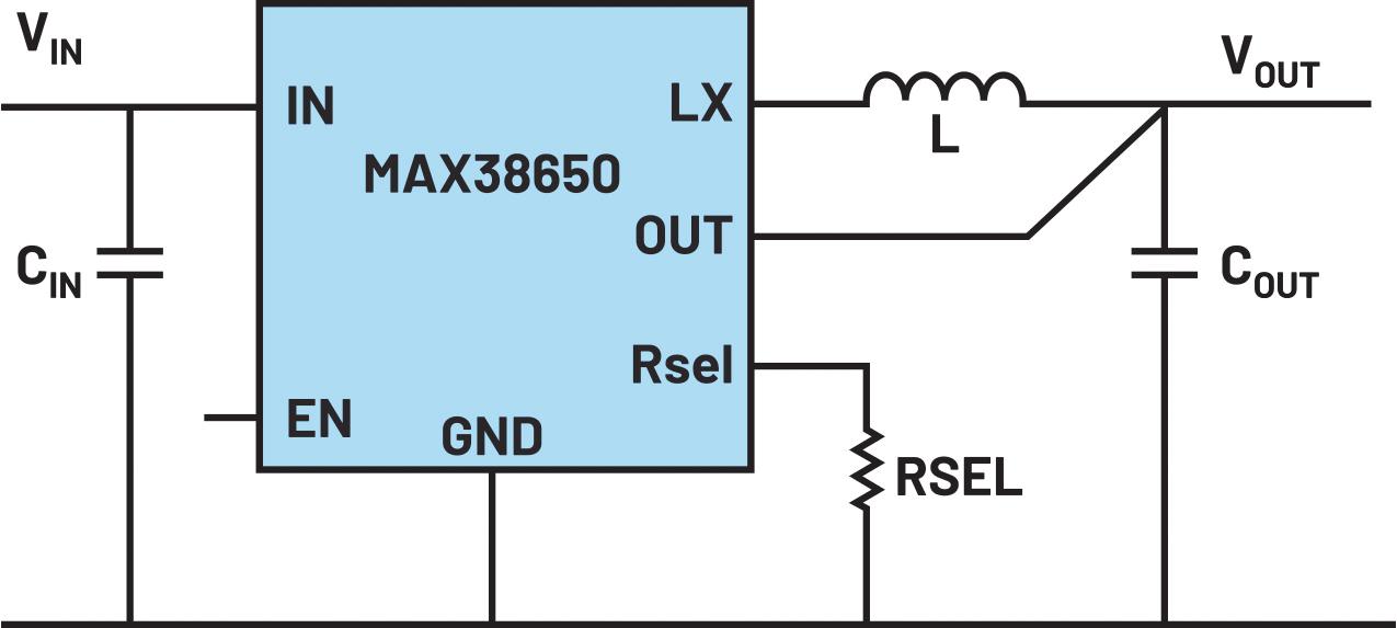
When the switching regulator is off, it draws a mere 5 nA. Sensor data is not acquired continuously, and communication is only necessary in the event of a fault. This means that the MAX38650 can often be switched to power-saving mode for additional energy savings.
Every basic voltage conversion circuit normally has a feedback pin. A simple resistor voltage divider is needed for the provision of a regulated output voltage. However, a resistor voltage divider doesn’t make much sense in an energy-saving circuit. Depending on the resistor values, either the current flow through the voltage divider is too high and leads to high losses or the resistor values are so high that the feedback node has a very high impedance. As a result, noise can couple into the feedback node and directly affect the regulation of the required voltage. Interference is especially a problem in industrial plants. As shown in Figure 2, the MAX38650 has an RSEL pin. It works with a single resistor, which sets the output voltage. When the MAX38650 is switched on, 200 μA of current is briefly passed through the external resistor.
While conducted interference can be greatly reduced with the help of additional filter circuits on the input side and the output side of the switched-mode power supply switching regulator, this is not quite that easy for radiated signal sources. A good board layout can protect against excessive interference radiation. Even then, residual noise coupling still exists in the system. This can only be reduced with good shielding, that is, a metal enclosure.
Pulsed current paths that occur in any switched-mode power supply are designed symmetrically so that the magnetic fields that arise largely cancel each other out.
This technology, in combination with flip chip technology, which eliminates bonding wires in the switching regulator IC, dramatically reduces radiated interference. Up to a 40 dB reduction in radiated interference is possible. This corresponds to a reduction in radiated power by a factor of ten thousand.
Figure 3 shows the symmetrical design of the Silent Switcher technology, with the simultaneously arising local pulsed currents shown in green. The pulsed currents generate pulsed magnetic fields with different polarities and cancel each other out for the most part.
The Silent Switcher technology is now in its third generation. In this generation, a special ultralow noise technology is also employed in ultralow noise linear regulators to reduce interference in the low frequency range, especially between 10 Hz and 100 kHz. This generation of Silent Switcher technology makes it possible in many applications to omit a filtering linear regulator between the switchedmode power supply switching regulator and the sensitive load.
WHEN SIZE PLAYS A KEY ROLESWITCHING REGULATORS WITH JUST ONE INDUCTOR
Some sensors need to be positioned in very tight spaces - especially when an existing sensor should be replaced with a modern Intelligent Edge sensor in the same spot.

However, such a shield is time-consuming to manufacture as well as cost-intensive. A switching regulator employing Silent Switcher® technology provides a very clever solution for minimizing the radiated interference.
Minimal radiated interference due to Silent
© ADI
Due to enhanced functionality, more electrical components are often also needed. As a result, innovative ways of reducing physical size must be found. An interesting example from the voltage
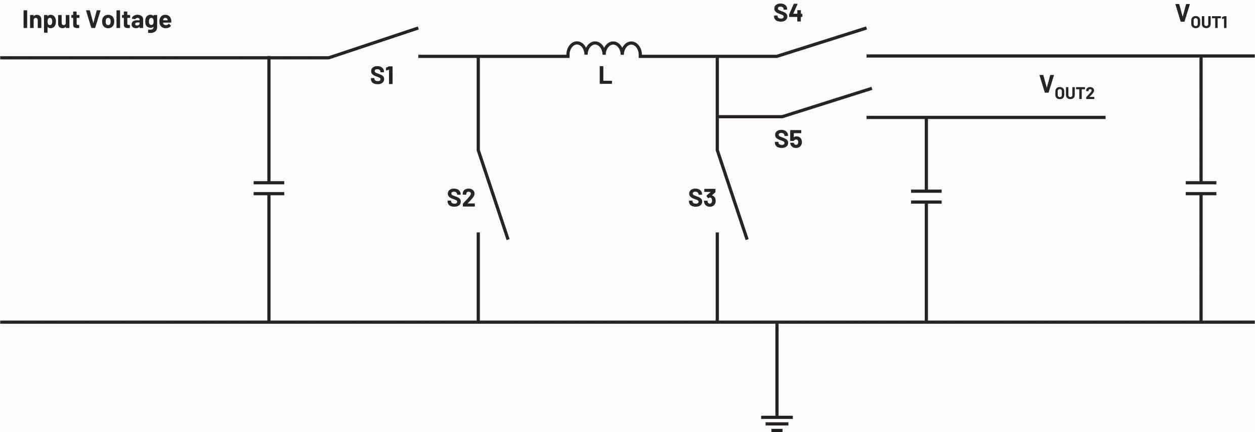
conversion world is the single-inductor, multiple-outlet (SIMO), which enables several different output voltages to be generated with a single inductor. The board space that would otherwise be taken up by multiple inductors can be saved with this.
Figure 4 shows an example of a simple SIMO regulator circuit for two precisely regulated output voltages. Additional supply voltages can be easily generated. Only one inductor, L, is needed. The SIMO technology can be implemented as follows: The single inductor is used successively for all individual output voltages. A certain amount of energy is placed in the inductor and then used to generate the voltage VOUT1. After that, another defined amount of energy is placed in the inductor and used to generate the voltage VOUT2. In this way, each generated voltage gets exactly the amount of energy needed to keep it stable.
Industrial Sensors Need
The innovations in the field of power supply described in this article all show how modern industrial sensors can be optimally supplied. Sensors are becoming more intelligent. The data they generate is already being evaluated locally at the Intelligent Edge.
More and more sensors are being used in industrial plants to help optimize processes and minimize downtime. To keep up with this trend, it will be necessary to employ innovative energy supply concepts such as energy harvesting.
■ Analog Devices www.analog.com


About the author Frederik Dostal is a power management expert with more than 20 years of experience in this industry. After his studies of microelectronics at the University of Erlangen, Germany, he joined National Semiconductor in 2001, where he worked as a field applications engineer, gaining a lot of experience in implementing power management solutions in customer projects. During his time at National, he also spent four years in Phoenix, Arizona (U.S.A.), working on switch-mode power supplies as an applications engineer. In 2009, he joined Analog Devices, where since then he held a variety of positions working for the product line and European technical support, and currently brings in his broad design and application knowledge as a power management expert. Frederik works in the ADI office in Munich, Germany.
Engage with like-minded members and ADI technology experts in our online community, EngineerZone®.
Expand your network, ask your tough design questions, share your expertise, browse our rich knowledge base, or read about new technologies and the engineers behind them in one of our blogs.
Visit https://ez.analog.com



Smartphone-enabled display pressure switches simplify both the commissioning process and the handling of spare parts.
Electronic pressure switches with display (display pressure switches) have existed for many years and are now available in a variety of versions. Considered in terms of the product life cycle, these products are now in the third stage of development: During the initial phase, new features and designs were the main focus, while cost-cutting measures marked the second phase. In the current third phase, the devices are equipped with additional connectivity (communication possibilities) and, in part, with their own intelligence. In addition to general technological developments, this development is mainly driven by the megatrends of the IoT and Industry 4.0, for a consistent networking of machine sensors to the ERP (Enterprise Resource Planning) system with the aim of “self-organized production”.
Trafag consistently pursued the mobile-first approach and placed the focus for the parameterization of the display pressure switch on the smartphone app. In contrast to the integrated 3-button operation with a 4-digit 7-segment display according to VDMA 24574-1, via the smartphone app one can navigate via the graphical user interface very quickly and intuitively through the parameterization. An integrated, configurable logger records the measured data, which can then also be sent via the app to the smartphone. In the industrial environment, these advantages of direct connection between humans and sensors over a smartphone can be used to increase efficiency and quality.
Parameterization during testing and commissioning Who doesn’t know that? The switch points and their parameters are defined by engineering, but during commissioning, it becomes clear that optimizations are still necessary, which are often determined in several loops. If the entire system can communicate via a bus system or IO-Link, this can be solved by the central controller. However, in spite of the great attention that these subjects are enjoying today, in reality most controllers on the sensor level communicate with conventional analog as well as digital signals and thus have no way of centrally controlling the parameterization of the pressure switches.
In such cases man comes to the rescue. This points to a general success factor of the display pressure switches: the user sees the current measured value and further information on the display and can adjust the switching points directly on the spot without interfering with the control. Thanks to the possibilities of a smartphone and the new App from Trafag it is now much easier to adjust the switching points. In addition, different parameter sets can be stored. In the case of test and optimization runs, a previously stored parameter profile can be loaded back to the pressure switch very quickly or sent to other measuring points. Compared to the conventional parameterization via VDMA three-button operations, this of course is much faster and more efficient, and thanks to the copying option, the error rate is significantly lower. Storing the clear-text-readable parameter sets also makes the documentation very simple and transparent.


Most machine and system manufacturers use display pressure switches, which, in addition to the switching outputs, also require analog outputs (for example 4 ... 20 mA, 0 ... 10 VDC) at various measuring points. Depending on the measuring point, the devices might differ only by means of the set switching points and the measuring range and consequently the analog signals. To facilitate the reduction of spare parts for maintenance, the Trafag display pressure switch DPC and DPS is ideal; besides the very simple parameterization by stored parameter sets, the 2:1 turn-down capability also helps to keep the spare parts to a minimum. It is possible to adjust the measuring range down to 50% of the nominal range as desired via the parameter sets, thus scaling the desired analog signal to the individual measuring range. The parameters can be adapted without power to the instrument! NFC (Near Field Communication), and not Bluetooth or WLAN, acts as the interface. This allows the replacement service or the service personnel to parameterize the instruments out of the box and unpowered. Otherwise it is also possible to check whether the correct parameter set is stored in the device before installation.
In addition to the above-mentioned advantages, the need for service is also simplified by the direct access of the employee to the device parameters - without intervention in the control system.


Thus, as a first error analysis, an employee of the operator can send the set parameters by e-mail to the customer service, which then checks whether the settings are correct. Another feature which is very useful in this case is the integrated logging function of the DPC / DPS, which records the applied trend of pressure and stores it in the device. This measured data can also be transferred via the NFC as a CSV file (Comma-separated Values) to the smartphone. This file may be sent by e-mail and be evaluated, for example by Excel, for system diagnostics.
In addition to system diagnostics, the integrated logger function offers even more interesting applications. For simple experimental setups - whether in the development of prototypes and function patterns, in testing or in laboratory experiments at colleges and universities - can be constructed without any additional equipment for measuring data acquisition: It only requires the connection of the DPC / DPS to a corresponding voltage supply, in order to then readout the measured data via the app. To connect the DPC / DPS display pressure switch to any power socket, Trafag offers a complete kit, available with a matching case and power adapter. Because the acquisition of pressure measurement data can be installed within a few minutes, the acquisition of measured data is also possible in situations where the installation of a conventional measurement data acquisition would not be worthwhile or where it would not be possible for logistical reasons (for example, because the service technician for the diagnosis can arrive with only limited luggage).
The downside of easy access to parameterization is, of course, the security issue. Here, however, the choice of NFC, with its close proximity range, offers considerable advantages over the other protocols WLAN or Bluetooth. Protocol that operate with greater proximity, are less secure, it is possible that access is gained from outside the factory, which makes complex encryption technologies necessary. Since NFC has a range of a few millimeters, it doesn›t work without direct access to the devices. The existing access rules are already sufficient to prevent access by outsiders. To ensure that unauthorized persons do not change any parameters, the access to the display pressure switch can be protected by means of a four-digit code, which also prevents NFC access. The presented examples show how the introduction of new technology, by the combining of smartphones and the electronic pressure switches, respectively, introduce new ways for enterprises to easily capture by a simple and efficient means, reducing inventory, bureaucracy and cost, to become more efficient repeatable and competitive.

Phone: +40 256-201346
E-mail: office@oboyle.ro www.oboyle.ro
