
11 minute read
NANOthermMA


There are huge sources of heat in the environment, which can be converted into electricity by thermoelectric materials. The NANOthermMA project aims to help researchers identify how materials can be engineered and nanostructured in order to improve thermoelectric performance, as Dr Neophytos Neophytou explains.
The development of thermoelectric materials opens up the possibility of generating electricity from temperature differences, an exciting prospect in the context of energy sustainability concerns. However, thermoelectric materials have traditionally been quite inefficient, and even current nanostructured materials - which provide a boost in performance - are not yet efficient enough for wider implementation, a topic Dr Neophytos Neophytou and his colleagues are addressing in the NANOthermMA project. “The goal in the project is to create a new class of more efficient nanostructured materials, building on theory, simulations and experiments,” he outlines. The thermoelectric performance of a material is quantified by the ZT figureof-merit. “The numerator in the ZT includes the electrical conductivity multiplied by the square of the Seebeck coefficient. This is what we call the power factor,” explains Dr Neophytou. “The denominator is the thermal conductivity, which determines the heat flow, resembling the losses in the process.”
A lot of attention has previously been focused on putting nanostructured features into a material to reduce thermal conductivity, so essentially reducing the denominator in the ZT figure-of-merit. While this has proved effective up to a point, there is only limited potential for further reductions, so Dr Neophytou and his colleagues are now taking a different approach. “The way to further improve
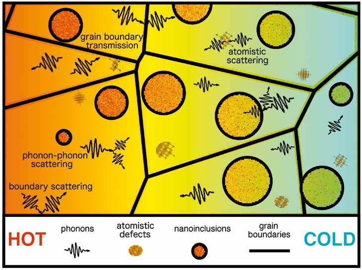
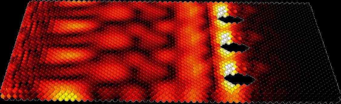
Nanostructured material geometry. Grain boundaries, nanoinclusions, and atomistic defects present obstacles for phonon transport (heat) as it propagates from the hot to the cold sides of a thermoelectric material.
efficiency is to work with the numerator, the power factor,” he outlines. There are some significant technical hurdles to overcome in this work however. “Nanostructuring reduces the electrical conductivity. We want to develop a nanostructure that doesn’t reduce the conductivity too much,” says Dr Neophytou. “There’s also an inherent relationship between the conductivity and the Seebeck coefficient – they are inversely proportional to each other.”
NANOthermMA project A material with a very high electrical conductivity will have a low Seebeck coefficient and vice-versa, and any effort to increase one will reduce the other. The aim of the project is to investigate how to effectively decouple this interdependence, which could eventually lead to the development of more efficient thermoelectric materials. “The inverse relation between conductivity and the Seebeck coefficient is strong, but there are ways that you can tweak that,” explains Dr Neophytou. This research is built on a deep understanding of material structure and how electrons and phonons flow through it. “If you zoom into a 3-d bulk material you will often find that it has a lot of grain boundaries, dislocations and defects. It’s a bulk material, but if you zoom in there internally, you find that it’s not a perfect crystal, it has a lot of defects,”
multi-scale geometries
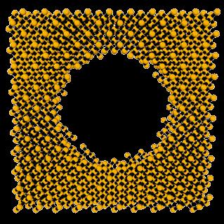
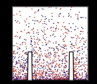
Zooming in a nanostructured thermoelectric material, where the matrix material is described in a continuum way, but the smaller defects are treated in an atomistic manner.


says Dr Neophytou. “Materials scientists also know how to create materials with a lot of nanostructured features.”
This opens up the possibility of modifying the material in certain ways to improve thermoelectric efficiency. If there are a lot of these grains and defects in a material then they slow down the flow of phonons, which describe thermal conductivity. “Phonons are vibrations of atoms in the material, and can be thought of as waves, or particles, that flow through a material,” outlines Dr Neophytou. Grains and defects also reduce the flow of electrons through a material and current. Doping a material – essentially introducing a different atomic element in the material and more mobile charges – enables researchers to minimise current reductions while also maintaining a high Seebeck co-efficient. “When you dope a material, these dopants act as additional scattering centres. If you can redistribute them so that they are concentrated in some regions of the material and not others then you have clean regions for electrons to flow,” explains Dr Neophytou. This is called modulation doping. The wider aim here is to direct the flow of electrons in the nanostructure
Nanostructuring has led to important improvements, but reduces the electrical conductivity. We want to develop nanostructures that don’t reduce the conductivity too much. There’s an inherent relationship between the conductivity and the Seebeck coefficient that we also want to break.

however, an issue Dr Neophytou and his colleagues are investigating in the project. “One idea we’re exploring to decouple electrical conductivity and the Seebeck coefficient is by effectively building barriers in the material,” he says. “A barrier is like a wall in the material that electrons have to jump over. Only the high-energy electrons will make it over – the low-energy ones will not. This is called energy filtering.”
The energy filtering approach leads to an increase in the Seebeck coefficient, yet it also leads to reduced electronic conductivity and relate the intrinsic properties of the material to the nanostructure geometry. “There is a link between how you design the nanostructure – such as the size of grains, the thickness of the grain boundaries, the height of the barrier walls – with the actual physical properties of the material, such as how the electrons interact with phonons,” says Dr Neophytou.
Materials scientists have recently developed the ability to create these features in nanostructures for a large number of materials, most of them consisting of complex characteristics and properties. Now the aim is to understand how they can be used to decouple the Seebeck coefficient and electrical conductivity. This research is largely theoretical in nature, and Dr Neophytou and his colleagues in the project are working with simulations. “We use multi-scale physics and multi-scale geometries. We start with fairly simple models, then we go to more accurate and elaborate semi-classical models to look at particle transport,” he outlines. “Then we go to much more sophisticated quantum transport models, looking at the behaviour of electrons in a quantum mechanical sense. Then we do the same thing for the heat, looking at phonons as particles and as waves. This is the simulation aspect of the work.”
This research could open up new insights into how to decouple the Seebeck coefficient and electrical conductivity in a material, while the project also has an experimental dimension. The aim with the experimental work is to create structures through which specific effects can be validated, so demonstrating the potential of nanostructured thermoelectric materials. “We have now identified three or four different things that have to be combined for this concept to work, and each provides its own performance boost in the power factor,” says Dr Neophytou. “We are trying to validate these different concepts through experiments. Our colleagues in the project are building ultra-thin structures, and then looking to verify whether they lead to a power factor improvement under certain conditions that we have proposed in the project.”
heat flow at the atomistic scale
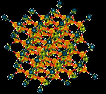
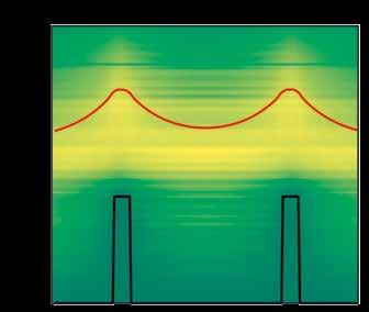
Snapshot of wave effects in heat flow as phonons encounter pore defects in a nanostructured thermoelectric material.

NANOthermMA Advanced Simulation Design of Nanostructured Thermoelectric Materials with Enhanced Power Factors Project Objectives The main objective is to resolve the on-going problem that limits the efficiency performance of thermoelectric materials, which is the inverse interdependence of the Seebeck coefficient and the electrical conductivity. The project establishes a theoretical strategy that relaxes the interdependence and achieves 5x efficiency improvements compared to state of the art, experimentally validates the theoretical propositions, and develops a large state-ofthe-art electrothermal simulator, open to the community, in order to guide the design of the novel nanostructured materials proposed. Project Funding ERC Starting Grant. Total funding: 1.5M Euro Project Partners My group is a theory and simulation group, and the project has experimental partners: • Professor Dario Narducci, University of Milano-Bicocca • Professor Giovanni Pennelli, University of Pisa Contact Details Project Coordinator, Dr Neophytos Neophytou School of Engineering University of Warwick T: +44 24 7652 3123 E: N.Neophytou@warwick.ac.uk W: https://warwick.ac.uk/fac/sci/eng/ research/grouplist/sensorsanddevices/ computational_nanotechnology_lab/ erc_nanothermma
Vassilios Vargiamidis and Neophytos Neophytou, ‘Hierarchical nanostructuring approaches for thermoelectric materials with high power factors’, Phys. Rev. B 99, 045405, (2019). Laura de Sousa Oliveira and Neophytos Neophytou, ‘Large-scale molecular dynamics investigation of geometrical features in nanoporous Si,’ Phys. Rev. B 100, 035409 (2019).
Dr Neophytos Neophytou
Dr Neophytos Neophytou is currently an Associate Professor at the School of Engineering, University of Warwick UK, where he runs the Computational Nanotechnology Lab. His area of specialization is theory, computational modelling and simulation of electronic and thermal transport in complex bandstructure materials, nanomaterials, nanodevices, and thermoelectric materials for energy conversion and generation.
e electron transport multi-physics
particles & classical n a n o s t r u c t u r i n g
(a) From the electrons’ point of view, nanostructuring builds potential energy barriers (‘walls’) that obstruct their flow. Only electrons with energies higher than the ‘wall’ can pass through. (b) Electrons as particles flowing in a superlattice material with potential barriers (red-right, blue-left). (c) Electrons as waves in the superlattice material.
Simulator The aim now is to build on the findings so far, and one part of the project involves developing a simulator which the research community can use to guide the design of the nanostructuring for their own materials, with a view to improving thermoelectric efficiency. This will allow researchers to identify the effects of nanostructuring on performance and assess how they correlate to a pristine material. “We aim to provide the community with a sort of nanostructure recipe that can decouple the conductivity and the Seebeck coefficient, so that you can increase both of them simultaneously. That will provide a huge boost in both the power factor and the figure of merit,” outlines Dr Neophytou. “A second major output will be to bring together all the computational tools that have been developed during the project and put them under a unified umbrella of a multi-physics, multi-scale, high-performance framework.”
This framework will have a very accessible interface with the user, allowing them to choose which simulation they want to run. A user will be able to choose the geometry, tools and physics relevant to their specific simulation, from which they can assess the performance of the structure. “It will be generic in the sense that we will put all these different tools there, but the user has to know what can be done in relation to the particular problem that they want to address. For example, if you want to simulate how the wave nature of electrons or phonons interacts with defects in a material, then you are bound to simulate quite small structures, but you can simulate larger structures with semi-classical tools,” says Dr Neophytou. “The tools that you can use are restricted by the nature of what you want to simulate. There is also scope to add more tools to the framework in the future.”

Applications for thermoelectrics The wider context here is the goal of improving the performance of thermoelectric materials, which hold a lot of potential in terms of addressing concerns around energy sustainability. There are many sources of heat in the environment, and Dr Neophytou says thermoelectric materials could be used to convert this heat into electricity. “There are many potential applications, such as microscavenging. For example flexible thermoelectrics are worn on clothes or skin, and they create electricity from the heat difference between your body and the surrounding environment to power small sensors. The materials can allow self-powered electronics in general without the need for a battery,” he explains.
Thermoelectric materials could also be used on larger energy scales. “Some car companies are working on creating a thermoelectric generator around the exhaust of the car. A third of the gas that is used in the car goes into motion, while the remainder is waste heat,” says Dr Neophytou.
Extracting some of this waste heat from a car’s exhaust and reusing it could greatly improve efficiency, while thermoelectric materials could also be used as heaters or coolers, or in car seats to improve comfort.
There are also many other potential applications in industrial processes, such as in the steel industry, which produces enormous quantities of waste heat. Cost is of course an important issue in terms of applying thermoelectric materials more widely. “It depends on the efficiency and price of the material,” acknowledges Dr Neophytou. Thermoelectric materials are already applied in certain areas, notably space missions, now by helping to improve the efficiency of cheaper materials Dr Neophytou hopes to encourage their use in a wider range of areas. “If the efficiency of cheap materials goes up, then there is the potential of scaling this to a wide range of technologies,” he says.


