Digital Systems Design Using Verilog 1st Edition Roth Solutions Manual Full clear download( no error formatting) at: https://testbanklive.com/download/digital-systems-design-using-verilog-1stedition-roth-solutions-manual/ Cha pter 2 : I ntroducti on to Veri log ® 2 . 1 ( a ) HDL – Har d war e De scr ip tio n La ng ua ge FP GA – Field P r o gr a mmab le Lo gic Ar r a y ( b) Ver ilo g has state me nts t hat ex ec ute co ncur r en tl y si nce it mu st mo d el r ea l har d war e in wh i ch the co mp o ne nt s ar e all in o p er atio n at the sa me t i me. ( c) A har d war e d escr ip tio n lan g uage al lo ws a d igi tal s yste m to b e d esigned and d eb u gge d at a hig her le vel o f ab str ac tio n t han sc he matic ca p t ur e wit h gates, flip - flo p s, and stand ar d MSI b uild in g b lo ck s. T he d etails o f t he gates a nd f lip - flo p s d o no t nee d to b e hand led d ur i n g ea r l y p hases o f d esi gn. Desi g ns ar e mo r e p o r tab le when lo w - l evel lib r ar y- sp ec ific d etails a r e no t incl ud ed in the mo d el. HDL s allo w t he cr ea tio n o f suc h p o r tab le hig h -leve l b ehavio r al mo d els.
2 . 2 ( a ) Le gal: A_123, _A123, c1 c2, and1; I llegal: 123A ( star ts wit h n u mb er ) , $ A123_ ( star ts wit h $ ) , and ( r eser ved wo r d ) . ( b) No ne o f the Ver ilo g id enti fier s ar e eq uivale nt si nce Ver ilo g is ca se se nsit ive. 2.3(a)
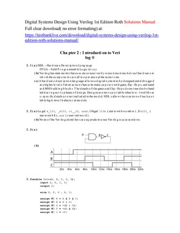
( b)
2 . 4 module Gate(A, B, C, D, Z); input A, B, C, D; output Z; wire E, F, G , H, I; assign assign assign assign assign
#5 #5 #5 #5 #2
H E G F I
= = = = =
A & H | ~(B ~(G ~F;
B & C; D; | C); & A);
assign #5 Z = E ^ I; endmodule
2 . 5 ( a ) module one_bit_sub(x, y, bin, diff , bout); input x, y, bin; outpu t diff, bout; assign diff = x ^ y ^ bin; assign bout = (~x & bin) | (~x & y) | (bin & y); endmodule
( b) module four_bit_sub(a, b, bin, d , bout); input[ 3:0] a, b;
input bin; output[ 3:0] d; output bout; wire[ 3:0] bo; one_bit_sub s1 (a[0], b[0], bin , d[0], bo[1]); one_bit_sub s2 (a[1], b[1], bo[ 1], d[1], bo[2]); one_bit_sub s3 (a[2], b[2], bo[ 2], d[2], bo[3]); one_bit_sub s4 (a[3], b[3], bo[ 3], d[3], bout); endmodule
2 . 6 ( a ) module circuit (A, B, C, D, G); input A, B , C, D; output G; wire E, F; assign E = A & B; assignF = E | C; assign G = D & F; endmodule
( b) module circuit (A, B, C, D, G); input A, B , C, D; output reg G; reg E, F; initial begin E <= 0; F <= 0; G <= 0; end always @(* ) begin E <= A & B; F<= E|C; G <= F & D; end endmodule
2 . 7 ( a ) A change s to 1 at 2 5 ns, B chan ges to 1 at 2 5 ns, C cha n ge to 1 at 3 5 ns ( b) A change s to 1 at 2 5 ns, B chan ges to 1 at 2 0 + Î&#x201D; ns, C d o es no t c han ge
2 . 8 ( a ) A falli n g-ed ge tr ig ger ed D flip - flo p wit h as yn chr o no us ac ti v e hig h clea r and set ( b) Q = '0 ', b ec ause C lr = 1 has p r io r it y.
2 . 9 module SR_Latch( S, R, Q, Qn);
input S, R; output reg Q; output Qn; initial begin Q <= 0; end
always @(S, R) begin if(S == 1'b1 ) Q <= 1'b1; if(R == 1'b1 ) Q <= 1'b0; end assign Qn = ~Q ; endmodule
2 . 1 0 module MNFF(M, N , CLK, CLRn, Q, Qn); input M, N, CLK , CLRn; output reg Q; output Qn; initial begin Q <= 0; end always @(CLK, CLRn) begin if(CLRn == 1'b0 ) begin Q <= 0; end else if(CLK == 0) begin if(M == 0 && N == Q <= ~Q ; else if(M == 0 && Q <= 1; else if(M == 1 && Q <= 0; else if(M == 1 && Q <= Q; end end
0)
N == 1) N == 0) N == 1)
assign Qn = ~Q ; endmodule
2 . 1 1 module DDFF(R, S , D, Clk, Q); input R, S, D, Clk; output reg Q; initial begin Q <= 0; end
always @(Clk, R, S) begin if(R == 1'b0 ) Q <= 0; else if(S == 1'b0) Q <= 1; else Q <= D; end endmodule
2 . 1 2 ( a ) module ITFF( I0, I1, T, R, Q, QN); input I0, I1, T, R; output reg Q; output QN; initial begin Q <= 0; end always @(T , R) begin if(R == 1'b1) #5 Q <= 0; else begin if((I0 == 1'b1 && T == 1'b1) || (I1 == 1'b1 && T == 1'b0 )) #8 Q <= QN; end end assign QN = ~Q; endmodule
( b) add list * add wave * force T 0 0, 1 100 -repeat 200 force I1 0 0, 1 50, 0 450 force I0 0 0, 1 450 run 750 ns
2.13 ns 10 20 20 25 35
Δ +0 +0 +1 +0 +0
a 0 0 0 1 5
b c d 0000 0001 7001 7001 7001
e
ns 10 20 20 25 35
Δ +0 +0 +1 +0 +0
a 0 0 0 1 5
b c d 0000 0001 7001 7001 7001
e
2.14
2 . 1 5 i. 5 ’b 1 01 0 1 ii. 8 ’b 1 1 01 0 10 1 iii. 3 ’b 100
2 . 1 6 i. 4 ’b 0 00 0
ii. 8 ’b 0 0 00 1 01 0 iii. 7 ’b 0 0 0 01 0 1
2.17
i. ii. iii. iv. v. vi. vii. viii.
8 ’h0 D 8’hFD 8’h5 0 8’h5 0 8’h0 D 8’hFD 8’h5 0 8’ h5 0
2.1 (a) 8
A >> 4 == 2’h0C A >> > 4 == 2’h FC A << 4 == 8’h70 A << < 4 == 8’h70
( b)
A >> 4 == 2’h0C A >> > 4 == 2’h0 C A << 4 == 8’h7 0 A << < 4 == 8 ’h7 0 A >> 4 == 2 ’h0 C A >> > 4 == 2 ’h 0 A << 4 == 8 ’h7 0 C A << < 4 == 8 ’h7 0
( c)
( d)
( e)
(f)
(g)
( h)
A >> 4 == 8 ’h0C A >> > 4 == 8 ’h0C A << 4 == 8 ’h70 A << < 4 = = 8 ’h70 A >> 4 == 8 ’h0 C A >> > 4 == 8 ’h0 C A << 4 == 8 ’h7 0 A << < 4 == 8 ’h7 0 A >> 4 == 8 ’h0 C A >> > 4 == 8 ’h FC A << 4 == 8 ’h7 0 A << < 4 == 8 ’h7 A 0 >> 4 == 8 ’h0 C A >> > 4 == 8 ’h FC A << 4 == 8 ’h7 0 A << < 4 == 8 ’h7 0 A >> 4 == 3 2 ’h0 FFF FF F C A >> > 4 == 3 2 ’hF FFF FF F A C<< 4 == 3 2 ’hFF FFF C7 0A << < 4 == 3 2 ’hF FFF FC7 0
2 . 1 9 i. 8’h0 D ii. 8 ’h0 D iii. 8 ’h5 0 iv. 8 ’h5 0 v. 8 ’h0 D
vi. 8 ’h0 D vii. 8 ’h5 0 viii. 8 ’ h5 0
2.20
i. ii. iii. iv. v. vi. vii. viii.
8 ’h0 D ’h5 8 ’h0 0 ’h5 8D 80 ’h0 D 8 ’h0 D 8 ’h5 08 ’ h5 0
2 . 2 1 T he s ynt hes ized har d war e is a 4 -b it shi ft r eg ister .
2 . 2 2 T he s ynt hes ized har d war e is a sin gle f lip - flo p .
2 . 2 3 B o th mo d ule s ar e s ynt hesized to 4 -b it shi ft r egi ster s. T her e ar e no d if fer ence s b et wee n t h e t wo s hi ft r egister s.
2 . 2 4 ( a ) D1 = 5 , D2 = 1 . T he values o f D1 and D2 s wap . ( b) D1 = 1 , D2 = 1 . T he values o f D1 and D2 d o no t s wap . ( c) iii
2 . 2 5 a ; y mu st b e in t he se nsit ivit y l ist , o ther wise su m and ca rry will no t up d ate fr o m c ha nge s to y
2.26 ns 0 5 5 5 6 10 10 10
2.27
Δ +0 +0 +1 +2 +0 +0 +1 +2
a 0 0 1 1 1 1 0 0
b c d 00000 00100 00100 11100 11000 11010 11010 00010
e
f
2.28
2.29(a) ns 0 4 5 10 15 20 25 30 35 40 45
abc 100 110 111 101 110 101 100 110 111 101 100
ns 0 4 5 10 15 20 25 30 35 40 45
abc 100 110 111 101 110 101 100 110 111 101 100
ns 0 4 9 10 15 20 25 30 35 40 45
abc 100 110 111 101 110 101 100 110 111 101 100
( b)
( c)
( d) ns 0 4 10 15 20 25 30 35 40 45
abc 100 110 100 110 101 100 110 111 101 100
2.30
2.31
2.32 ns 4 5 10 10 11 12 15
Î&#x201D; +0 +0 +0 +1 +0 +0 +0
a 0 1 1 0 0 0 0
b c 000 000 100 100 101 111 011
d
2 . 3 3 ( a ) 6 ’b 1 1 1 01 1 ( b) 3 ’b 0 0 1 ( c) 3 ’b 0 0 1 ( d) 1 ’b 0 ( e) 3 'b 1 1 1
2.34(a)
( b)
2.35
2.3 6
Clr is as yn chr o no us, wh er ea s C af f ec ts a s ync hr o no us i np u t to the D flip - flo p .
2 . 3 7 ( a ) assign #10 F = (C == 0)? ((D==0)? ~A: B):((D==0)? ~B: 0); ( b) always @(*) begin if(C== 0 && D==0) #10 F = ~A; else if(C==0 && D==1) #10 F = B; else if(C==1 && D==0) #10 F = ~B; else #10 F = 0; end
( c) always @(*) begin case( sel) 0: #10 1: #10 2: #10 3: #10 endcase end
F F F F
= = = =
~A; B; ~B; 0;
2 . 3 8 ( a ) mo d ule 1 : always @(C, B1, B2, B3) begin if (C == 1) A <= B1; else if (C == 2) A <= B2; else if (C == 3) A <= B3; else A <= 0; end
mo d ule 2 : assign A = (C==1)? B1 : ((C==2)? B2 : ((C==3)? B3 : 0 ));
( b)
2 . 3 9 ( a ) module SR_Latch(S, R, P, Q); input S, R; output P, Q; assign Q = (S)? 1 : ((R)? 0 : Q); assign P = ~Q; endmodule
( b) assign Q = S | (~R & Q); assign P = ~Q;
( c) assign Q = ~(R | P); assign P = ~(S | Q);
2 . 4 0 i. 8 ’b 00 0 10 1 00 ii. 8 ’b 0 00 1 01 0 0 iii. 8 ’b 1 1 11 1 10 0 iv. 8 ’b 1 1 1 11 1 00 v. 8 ’b 0 0 01 0 10 0 vi. 8 ’b 0 0 0 10 1 00
2 . 4 1 i. 32 ’hFF FFF F5 B ii. 32 ’hF FFF FF5 B iii. 3 2 ’h0 0 0 0 01 5 B iv. 3 2 ’h0 0 0 0 0 15 B v. 3 2 ’h0 0 0 0 00 5 B vi. 3 2 ’h0 0 0 0 0 05 B
2.42(a)
( b)
( c) module comp4bit(A, B, EQin, GTin , LTin, EQout, GTout, LTout ); input[ 3:0] A, B; input EQin, GTin, LTin; output reg EQout, GTout, LTout ; initial EQout GTout LTout end
begin = 0; = 0; = 0;
always @(A, B, EQin, GTin, LTin ) begin if( A > B) begin EQout <= 0; GTout <= 1; LTout <= 0; end else if(A < B) begin EQout <= 0; GTout <= 0; LTout <= 1; end else if(GTin == 1) begin EQout <= 0; GTout <= 1; LTout <= 0; end else if(LTin == 1) begin EQout <= 0; GTout <= 0; LTout <= 1; end else begin EQout <= 1; GTout <= 0; LTout <= 0; end end endmodule
( d) module comp8bit(A, B, EQi, GTi, LTi, EQ, GT, LT); input[ 7:0] A, B; input EQi, GTi, LTi; output EQ, GT, LT;
w i r e L o w E Q , L o w G T , L o w L T ; c o m p 4 b i t C 1 ( A [ 3 : 0 ] , B [ 3 : 0 ] , E Q i , G T i , L T i , L o w E
Q, LowGT , LowLT); comp4bit C2 (A[7:4], B[7:4], LowEQ , LowGT, LowLT, EQ, GT , LT); endmodule
2 . 4 3 module shift_reg (SI, EN, CK, SO); input SI, EN , CK; output SO; reg[15:0] register ; initial begin register <= 0; end always @(posedge CK) begin if(EN == 1 ) register <= {SI, register[15:1]}; end assign SO = register[0]; endmodule
2 . 4 4 ( a ) module shift74194(D, S, SDR, SDL , CLRb, CLK, Q); input[ 3:0] D; input[ 1:0] S; input SDR, SDL, CLRb, CLK; output reg [3:0] Q; initial begin Q <= 0; end always @(CLK, CLRb) begin if( CLRb == 0) Q <= 4'b0000; else if(CLK == 1) begin case( S) 0 : Q <= Q; 1 : Q <= {Q[2:0],SDL}; 2 : Q <= {SDR, Q[3:1]}; 3 : Q <= D; endcase end end endmodule
( b)
module bit8shift(X, S, RSD, LSD, CLRb, CLK, Y); input[ 7:0] X; input[ 1:0] S; input RSD, LSD, CLRb, CLK; output [7:0] Y; shift74194 S1 (X[3:0], S, Y[4], LSD, CLRb, CLK, Y[3:0]); shift74194 S 2(X[7:4], S, RSD, Y[3], CLRb, CLK, Y[7:4]); endmodule
2.45
(a)
module Counter(D, CLK, CLR, ENT, ENP, UP, LOAD, Q, CO); input[ 3:0] D; input CLK, CLR, ENT, ENP, UP, LOAD; output reg[3:0] Q; output CO; initial begin Q = 0; end assign CO = ((ENT == 1) && ((UP == 1 && (Q == 4'b1001)) || (UP == 0 && (Q == 4'b0000)))); always @(CLK, CLR) begin if( CLR == 0) Q <= 0; else if(CLK == 1) begin if( LOAD == 0) Q <= D; else if(ENT == 1 && ENP == 1 && UP == 0) begin if(Q == 0) Q <= 4'b1001; else Q <= Q - 1; end else if(ENT == 1 && ENP == 1 && UP == 1) begin if(Q == 4'b1001) Q <= 0; else Q <= Q + 1; end end end endmodule
( b) module Century_Counter(Din1, Din2 , CLK, CLR, ENT, ENP, UP , LOAD, Count, CO); input [3:0] Din1, Din2; input CLK, CLR, ENT, ENP, UP, LOAD; output [7:0] Count; output CO; wire [3:0] Qout1, Qout2; wire Carry1, Carry2;
Counte r ct1(Din1, CLK, CLR, ENT , ENP, UP, LOAD, Qout1, Carry1); Counter ct2 (Din2, CLK, CLR, ENT , Carry1, UP, LOAD, Qout2 , Carry2);
assign Count = {Qout2, Qout1}; assign CO = Carry2; endmodule
T he b lo ck d iagr am i s si milar t o Figur e 2 -45 wit h an " Up " inp ut a d d ed to ea ch co unter . ( c) add wave * force Din2 4'b1001 force Din1 4'b1000 force CLK 0 0 ns, 1 50 ns -repeat 100 ns force CLR 1 0 ns, 0 1000 ns force LOAD 0 0 ns, 1 100 ns force ENT 1 0 ns, 0 400 ns, 1 600 ns force ENP 1 force UP 1 0 ns, 0 500 ns run 1200 ns
2 . 4 6 Stud e nts s ho uld lo o k o n the web fo r 7 4 HC1 9 2 d ata shee t. CL R is ac tive hi g h. LO ADB is ac tive lo w. Co un tin g up hap p ens when UP has a r isi n g ed ge a n d DOW N= 1 . Co unti n g d o wn hap p ens wh e n DOW N ha s a r isi n g ed ge and UP =1 . C AR RY i nd ica tes ter mi nal co unt in t he up d ir ec tio n , i.e . 9 . B ORROW ind icate s ter mi nal co u nt in t he d o wn d ir ec t io n, i.e . 0 . Op er ating Mo d e Clear Lo ad Co u nt U p Co u nt D o wn
CL R LO ADB UP DOW N D 1 X X 0 XXXX 1 X X 1 XXXX 0 0 X X XXXX 0 1 ↑ 1 XXXX 0 1 1 ↑ XXXX
Q B o r ro w Car r y 0000 0 1 0000 1 1 Q = D 1* 1* Q = Q + 1 1 1 ** Q = Q – 1 1 ** 1
* whe n lo ad in g, i f t he inp ut is 0 and d o wn = 0 , b o r r o w wi ll b e 0 . I f the inp u t is 9 and up = 0 , ca r r y wil l b e 0 ** B o r r o w = 0 whe n the co un ter is in state 0 and d o wn = 0 . Car r y = 0 when t h e co unter is in state 9 and up = 0 . module count74HC192 (DOWN, UP, CLR, LOADB , BORROW, CARRY, D, Q); input DOWN, UP , CLR, LOADB; input[3:0] D; output BORROW, CARRY; output reg[3:0 ] Q; initial begin Q = 0; end always @(DOWN, UP, CLR, LOADB) begin if(CLR == 1) Q <= 0; else if(LOADB == 0) Q <= D; else if(DOWN == 1) begin @(posedge UP) if(Q == 4'b1001 )
Q <= 0; else Q <= Q + 1; end else if(UP == 1) begin @(posedge DOWN)
if(Q == 0) Q <= 4'b1001 ; else Q <= Q - 1; end end assign BORROW = (DOWN == 0 && Q == 0)? 0 : 1; assign CARRY = (UP == 0 && Q == 4'b1001 )? 0 : 1; endmodule
2 . 4 7 ( a ) module shift8(Q, D, CLR, CLK, S0 , S1, LSI, RSI); input[ 7:0] D; output reg[7:0] Q; input CLR, CLK, S0, S1, LSI, RSI ; initial begin Q = 0; end always @(CLK, CLR) begin if( CLR == 1) Q <= 0; else if(CLK == 1) begin if( S0 == 1 && S1 ==1) Q <= D; else if(S0 == 0 && S1 == 1 ) Q <= {RSI, Q[7:1]}; else if(S0 == 1 && S1 == 0 ) Q <= {Q[6:0], LSI}; else Q <= Q; end end endmodule
( b)
No te: D is no t s ho wn i n t he d iagr a m.
( c) module shiftreg(QQ, DD, CLK2, CLR2 , L, R); input[ 15:0] DD; input CLK2, CLR2, L, R;
output[ 15:0] QQ; shift8 SR1 (QQ[15:8], DD[15:8], CLR2, CLK2, L, R, QQ[7], QQ[0]); shift8 SR2 (QQ[7:0], DD[7:0], CLR2 , CLK2, L, R, QQ[15], QQ[8]); endmodule
2 . 4 8 module countQ1 (clk, Ld8, Enable, S5, Q); input clk, Ld8 , Enable; output S5; output[3:0] Q; reg[3:0] Qint ; initial begin Qint = 0; end always @(posedge clk) begin if(Ld8 == 1) Qint <= 4'b1000; else if(Enable == 1) begin if(Qint == 4'b0011) Qint <= 4'b1000; else Qint <= Qint - 1; end end assign S5 = (Qint == 4'b0101)? 1 : 0; assign Q = Qint ; endmodule
2 . 4 9 ( a ) module up_down(CLK, CLR, LD, UP, D, Q); input CLK, CLR, LD, UP; input[ 3:0] D; output reg[3:0] Q; initial begin Q = 0; end always @(negedge CLK) begin if( CLR == 1) Q <= 4'b0000; else if(LD == 1) Q <= D; else if(UP == 1) Q <= Q + 1; else Q <= Q - 1; end endmodule
( b)
( c) module modulo6(CLK, Reset, CNT, Q); input CLK, Reset, CNT; output[ 3:0] Q; wire load, clock; assign load = Reset | (~Q[0] & Q[1] & Q[2] & ~Q[3]); assign clock = CLK & CNT; up_down U1 (clock, 1'b0, load, 1'b1, 4'b0001, Q); endmodule
2.50(a)
( b)
P r esent State S0 S1 S2 S3
Next State
X=0X=1
X=0X=1
Z1 Z2 Z1 Z2
S0 S1 S1 S2 S2 S3 S0 S1
1000 0101 0101 0010
2 . 5 1 T he fo llo wi ng so lut io ns utiliz e the so lu tio n fo r 1.13. ( a ) module P2_51a(X, CLK, S, V); input X, CLK; output S, V; reg [ 2:0] StateTable0 [5:0]; reg [ 2:0] StateTable1 [5:0]; reg [ 1:0] OutTable0 [5:0]; reg [ 1:0] OutTable1 [5:0];
reg [ 2:0] State; wire [2:0] NextState;
initial begin StateTable0 [0] <= 1; StateTable1 [0] <= 1; StateTable0 [1] <= 2; StateTable1 [1] <= 4; StateTable0 [2] <= 3; StateTable1 [2] <= 3; StateTable0 [3] <= 0; StateTable1 [3] <= 0; StateTable0 [4] <= 3; StateTable1 [4] <= 5; StateTable0 [5] <= 0; StateTable1 [5] <= 0; OutTable0 [0] <= 2'b00; OutTable1 [0] <= 2'b10; OutTable0 [1] <= 2'b10; OutTable1 [1] <= 2'b00; OutTable0 [2] <= 2'b00; OutTable1 [2] <= 2'b10; OutTable0 [3] <= 2'b00; OutTable1 [3] <= 2'b10; OutTable0 [4] <= 2'b10; OutTable1 [4] <= 2'b00; OutTable0 [5] <= 2'b10; OutTable1 [5] <= 2'b01; State <= 0; end assign NextState = (X==0)? StateTable0 [State] : StateTable1 [State]; assign S = (X==0)? OutTable0[State ][1] : OutTable1[State ][1]; assign V = (X==0)? OutTable0[State ][0] : OutTable1[State ][0]; always @(negedge CLK) begin State <= NextState; end endmodule
exa mp le s i mula tio n co mma nd s: add wave * force CLK 1 0 ns, 0 10 ns -repeat 20 ns force X 1 0 ns, 0 15 ns, 1 35 ns, 0 75 ns, 1 95 ns, 0 175 ns run 240 ns
( b) module P2_51b(X, CLK, S, V); input X, CLK; output S, V; reg Q1 , Q2, Q3; initial Q1 <= Q2 <= Q3 <= end
begin 0; 0; 0;
always @(negedge CLK) begin Q1 <= (~Q1 & Q3); Q2 <= (~Q2 & ~Q3) | (X & ~Q1 & Q2); Q3 <= (~Q1 & Q3) | (Q2 & ~Q3 ); end assign S = (X & ~Q2) | (~X & Q2 ); assign V = (X & Q1 & Q2); endmodule
Rea d ea ch set o f o utp u ts af ter 1 /4 clo ck p er iod b efo r e the fal lin g ed ge o f the clo ck b u t no later than t he falli ng ed ge o f t he clo ck .
( c) module P2_51c(X, CLK, S, V); input X, CLK; output S, V; wire wire wire wire
Q1, XN, D1, A1,
Q2, Q3; Q1N, Q2N, Q3N; D2, D3; A2, A3, A4, A5, A6;
Inverter I1 (X, XN); And2 G1 (Q1N, Q3, D1); And2 G2 (Q2N, Q3N, A1); And3 G3 (X, Q1N, Q2, A2); Or2 G4 (A1, A2, D2); And2 G5 (Q1N, Q3, A3); And2 G6 (Q2, Q3N, A4); Or2 G7 (A3, A4, D3); And2 G8 (X, Q2N, A5); And2 G9 (XN, Q2, A6); Or2 G10 (A5, A6, S); And3 G11 (X, Q1, Q2, V); DFF DFF1 (D1, CLK, Q1,Q1N); DFFDFF2 (D2, CLK, Q2, Q2N); DFF DFF3 (D3, CLK, Q3, Q3N); endmodule
See Sectio n 2 . 1 5 fo r the d efinitio n o f t he DFF co mp o nent. T he And3, And2 , Or2, and Inverter co mp o ne nt s ar e all si mi lar to the Nand3 co mp o nent gi ven o n p ages 1 0 9 -110 ( sec tio n 2 . 1 5 ) .
2. 5 2 T he fo llo wi ng so lut io ns utiliz e the so lu tio n fo r 1 .14. ( a ) module P2_52a(X, CLK, D, B); input X, CLK; output reg D, B; reg[2 :0] State, NextState; initial begin State <= 0; NextState <= 0; end always @(State, begin case( State) 0:begin if( X == 0) begin D <= 0; B NextState end else begin D <= 1; B NextState
X)
<= 0; <= 1;
<= 0; <= 1;
end end 1:begin if( X == 0) begin D <= 1;
B <= 0; NextState end else begin D <= 0; B NextState end end 2: begin if( X == 0) begin D <= 1; B NextState end else begin D <= 0; B NextState end end 3: begin if( X == 0) begin D <= 0; B NextState end else begin D <= 1; B NextState end end 4: begin if( X == 0) begin D <= 1; B NextState end else begin D <= 0; B NextState end end 5: begin if( X == 0) begin D <= 0; B NextState end else begin D <= 1; B NextState end end endcase end
<= 2;
<= 0; <= 3;
<= 0; <= 4;
<= 0; <= 5;
<= 0; <= 5;
<= 0; <= 5;
<= 1; <= 0;
<= 0; <= 0;
<= 0; <= 0;
<= 0; <= 0;
always @(negedge CLK) begin State <= NextState; end endmodule
exa mp le si mula tio n co mma nd s: add wave * force CLK 1 0 ns, 0 1 0 ns -repeat 20 ns force X 1 0 ns, 0 15 ns, 1 35 ns, 0 75 ns, 1 95 ns, 0 175 ns run 240 ns
( b) module P2_52b(X, CLK, D, B); input X, CLK; output D, B; reg Q1 , Q2, Q3; initial Q1 <= Q2 <= Q3 <= end
begin 0; 0; 0;
always @(negedge CLK) begin Q1 <= (~Q1 & ~Q3) | (~X & Q1 & ~Q2); Q2 <= (~Q2 & Q3); Q3 <= ~Q2 & (Q3 | Q1); end assign D = (~X & Q1) | (X & ~Q1 & Q3); assign B = ~X & Q1 & Q2; endmodule
Rea d ea ch set o f o utp u ts af ter 3 /4 clo ck p er iod b efo r e the fal li n g ed ge o f the clo ck b u t no later than t he falli ng ed ge o f t he clo ck. ( c) module PC_52c(X, CLK, D, B); input X, CLK; output D, B; wire A1, A2, A3; wire Q1, Q2, Q3; wire Q1N, Q2N, Q3N, XN, One; parameter I = 1; Inverter I1 (X, XN); Nand2 G 1(XN, Q2N, A1); JKFF FF1 (I, I, Q3N, A1, CLK, Q1 , Q1N); JKFF FF2 (I, I, Q3, I, CLK, Q2, Q2N); JKFF FF3 (I, I, Q1, Q2, CLK, Q3 , Q3N); Nand2 G2 (XN, Q1, A2); Nand3 G3 (X, Q1N, Q3, A3); Nand2 G4 (A2, A3, D); And3 G5 (XN, Q1, Q2, B); endmodule
T he Nand2, And3 , and Inverter co mp o ne nts ar e si milar to the Nand3 co mp o nent i n Sectio n 2 . 1 5 . T he JKFF co mp o ne nt i s si milar to the DFF co mp o ne nt in Sectio n 2 . 1 5 .
2. 53 module moore_mach (X1, X2, Clk, Z); input X1, X2 ; input Clk; output Z; reg[1:0] state ; initial begin state <= 1 ; end always @(negedge Clk) begin case(state ) 1: begin if((X1 ^ X2) == 1)begin #10 state <= 2; end end 2: begin if(X2 == 1)begin #10 state <= 1; end end default: begin end endcase end assign #10 Z = state[1]; endmodule
2. 54 module P_54(x1 , x2, clk, z1, z2); input x1, x2 , clk; output z1, z2 ; reg[1:0] state , next_state; initial begin state <= 1 ; next_state <= 1; end always @(state , x1, x2) begin case(state ) 1: begin if({x1,x2 } == 2'b00) #10 next_state <= 3; else if({ x1,x2} == 2'b01) #10 next_state <= 2; else #10 next_state <= 1; end 2: begin
if({x1,x2 } == 2'b00) #10 next_state <= 2; else if({ x1,x2} == 2'b01) #10 next_state <= 1; else #10 next_state <= 3;
end 3: begin if({x1,x2 } == 2'b00) #10 next_state <= 1; else if({ x1,x2} == 2'b01) #10 next_state <= 2; else #10 next_state <= 3; end endcase end always @(negedge clk) begin #5 state <= next_state; end assign #10 z1 = (state == 2)? 1: 0; assign #10 z2 = (state == 3)? 1: 0; endmodule
2 . 5 5 ( a ) ne xtsta te is no t al wa ys ass ig n ed a ne w val ue i n the co nd iti o nal state me nts, i.e . else cla u ses ar e no t sp ec ified . T her efo r e, a latch will b e cr ea ted to ho ld n ex tsta te to its o ld value. ( b) T he latch o utp ut wo uld ha ve t he mo s t r ec ent va lue o f n ex tst a te . ( c) always @(state, X) begin case( state) 0: begin if( X == 1) nextstate else nextstate end 1: begin if( X == 0) nextstate else nextstate end 2: begin if( X == 1) nextstate else nextstate end endcase end
<= 1; <= 0;
<= 2; <= 1;
<= 0; <= 2;
( d) Yes, u nco nd itio na ll y set n ex tst a te to a d efault val ue at the b e gin ni n g o f t he al wa ys b lo ck
2. 56 T he no nb lo cki ng as sig n me nt s mu st b e c han ged to b lo cki ng ass ig n men ts . Ot her wi se s el will no t up d ate fo r cur r e nt use. sel up d ates o nl y at t he e nd o f the p r o ce ss so t he ca se state me nt wil l get t he wr o n g va lue.
2. 57 ns 0 5 15 15 25 25 35 35 40
Î&#x201D; +0 +0 +0 +1 +0 +1 +0 +1 +0
A 0 1 1 1 1 1 1 1 0
B D 00 00 01 11 10 00 01 11 11
2. 58 Risi n g-ed ge tr ig ger ed to gg le f lip -f lo p (T -flip -f lo p ) , wit h as ynchr o no us ac ti ve -h ig h clea r si gnal
2. 59 ( a ) module ROM4_3(ROMin, ROMout); input[ 3:0] ROMin; output[ 2:0] ROMout; reg[2 :0] ROM16X3 [15:0]; initial begin ROM16X3 [0] <= 3'b000; ROM16X 3[1] <= 3'b001; ROM16X3 [2] <= 3'b001; ROM16X3 [3] <= 3'b010; ROM16X3 [4] <= 3'b001; ROM16X3 [5] <= 3'b010; ROM16X3 [6] <= 3'b010; ROM16X3 [7] <= 3'b011; ROM16X3 [8] <= 3'b001; ROM16X3 [9] <= 3'b010; ROM16X3 [10] <= 3'b010; ROM16X3 [11] <= 3'b011; ROM16X3 [12] <= 3'b010; ROM16X3 [13] <= 3'b011; ROM16X3 [14] <= 3'b011; ROM16X3 [15] <= 3'b100; end assign ROMout = ROM16X3[ROMin]; endmodule
( b) module P_59(A, count); input[ 11:0] A; output[ 3:0] count; wire[ 2:0] B,C,D; ROM4_3 R1 (A[11:8], B); ROM4_3 R2 (A[7:4], C); ROM4_3 R3 (A[3:0], D);
assign count = {1'b0, B} + C + D; endmodule
( c)
2.60 a 0 0 0 0 1 1 1 1
b 0 0 1 1 0 0 1 1
A 1 1 1 11 1 11 1 11 1 0 1 0 11 0 10 1 10 1 1 0 0 00 1 01 1 10 0 c y7 y6 y5 0 0 0 0 1 0 0 0 0 0 0 0 1 0 0 0 0 0 0 0 1 0 0 1 0 0 1 0 1 1 0 0
Co u nt 1100 0111 0101
DCB 100 100 100 011 010 010 010 010 001
y4 0 0 0 0 1 0 0 0
y2 0 0 1 0 0 0 0 0
y3 0 0 0 1 0 0 0 0
y1 0 1 0 0 0 0 0 0
y0 1 0 0 0 0 0 0 0
module decoder (A, B, C, Y); input A,B,C; output[7:0] Y; wire[2:0] index ; reg[7:0] ROM [0:7]; initial begin ROM[0] <= 8'b00000001; ROM[1] <= 8'b00000010; ROM[2] <= 8'b00000100; ROM[3] <= 8'b00001000; ROM[4] <= 8'b00010000; ROM[5] <= 8'b00100000; ROM[6] <= 8'b01000000; ROM[7] <= 8'b10000000; end assign index = {A,B,C}; assign Y = ROM [index]; endmodule
2. 61 ( a ) always begin MAX = A[0]; for ( i = 0; i < 20; i = i + 1) begin if( A[i] > MAX) MAX = A[i]; end end
( b) always begin MAX = A[0]; i = 1 ; while (i < 20) begin if( A[i] > MAX) MAX = A[i];
i = i + 1; end end
2. 62 module tester; reg CLK; reg [0:11] X ; reg [0:11] Z ; initial begin X = 12'b011011011100 ; Z= 12'b100110110110 ; CLK = 1; end reg Xin; wire Zout; integer i; always #50 CLK = ~CLK; Mealy M1(Xin , CLK, Zout); always begin for(i = 0; i < 12; i = i + 1) begin @(posedge CLK) #10 Xin = X[i]; #80 // wait to read outpu t if( Zout != Z[i]) begin $display ("Error"); $stop; end end $display("sequence correct" ); $stop; end endmodule
2 . 6 3 module TestExcess3 ; reg[3:0] XA[ 1:10]; reg[3:0] ZA[ 1:10]; reg X, CLK; wire Z; integer i; integer j; initial begin X = 0; CLK = 0; XA[1] = 4'b0000 XA[2] = 4'b0001 XA[3] = 4'b0010 XA[4] = 4'b0011 XA[5] = 4'b0100 XA[6] = 4'b0101 XA[7] = 4'b0110 XA[8] = 4'b0111 XA[9] = 4'b1000
; ; ; ; ; ; ; ; ;
XA[10] = 4'b1001 ; ZA[1] = 4'b0011 ZA[2] = ; 4'b0100 ZA[3] = ; 4'b0101 ZA[4] = ; 4'b0110 ZA[5] = ; 4'b0111 ZA[6] = ; 4'b1000 ;
ZA[7] = 4'b1001 ; ZA[8] = 4'b1010 ; ZA[9] = 4'b1011 ; ZA[10] = 4'b1100 ; end always #50 CLK <= ~CLK; Code_Converter C1 (X, CLK, Z); always begin for(i = 1 ; i <= 10; i = i + 1) begin for(j= 0 ; j <= 3; j = j + 1) begin X = XA [i][j]; @(posedge CLK); #(25); if(ZA[ i][j] != Z) begin $display ("sequence incorrect" ); $stop ; end end end $display("all sequences correct" ); $stop; end endmodule
2. 64 module testbench ; wire S5; reg clk, Ld8 , Enable; wire[3:0] Q; initial begin clk = 1; Ld8 = 1; Enable = 0 ; #100 Ld8 = 0; Enable = 1 ; #500 Enable = 0; #200 Enable = 1; #1000 Enable = 0; end always #50 clk <= ~clk; always @(posedge S5) $display ($time); countQ1 C1(clk , Ld8, Enable, S5, Q);
endmodule
2. 65 module testSMQ1 (correct); output reg correct ; reg clk, X; integer i; wire Z; reg[1:5] answer ;
initial begin answer[1] = 1; answer[2] = 1; answer[3] = 0; answer[4] = 1; answer[5] = 0; clk = 0; X = 1; #100 X = 0 ; #200 X = 1 ; end always #50 clk <= ~clk; SMQ1 S1(X, clk , Z); always begin for(i = 1; i <= 5; i = i + 1) begin @(posedge clk); correct = (answer[i] == Z); if(correct == 0) $displa y($time); #10; end $stop; end endmodule
Digital Systems Design Using Verilog 1st Edition Roth Solutions Manual Full clear download( no error formatting) at: https://testbanklive.com/download/digital-systems-design-using-verilog-1stedition-roth-solutions-manual/ digital system design using verilog by charles roth pdf digital system design using verilog solution manual digital systems design using verilog pdf digital systems design using verilog solution digital systems design using verilog roth digital system design using verilog by ashenden pdf digital systems design using vhdl 2nd edition charles roth verilog digital system design