1 minute read
International Journal for Research in Applied Science & Engineering Technology (IJRASET)

ISSN: 2321-9653; IC Value: 45.98; SJ Impact Factor: 7.538
Advertisement
Volume 11 Issue IV Apr 2023- Available at www.ijraset.com
The resistor of differentiator is connectedto Vcc to generate negative trigger pulses and the diode avoids positive spikes. And now this output is modulated using the input voltage applied at the control pin of the IC. So, whenever the Trigger pin pulses become low the output of the IC switchesto high and as a result the discharge transistor (internal to the 555 IC attached to the 7th pin) is disabled. So C2 charges through R2. This capacitor keeps on charging until the voltage is above the input control voltage, at which the IC changes its state. Now the output is low which makes the discharge transistor activated thereby discharging the capacitor C2. Hence the output pulse width is determined by the control voltage. This process continues, and we get a continuous stream of pulses which can be usedfor motor control, driving LED’s, transmitting servo signals for remote control applications etc. An insulated gate bipolar transistor (IGBT) is a device in which a IGBT is combined with a bipolar transistor. The utility model has the advantages that the power IGBT is easy to drive, the control is simple, the switching frequency is high, and the power transistor has low on-voltage, large on-state current and small loss. According to Toshiba, the on-resistance of the 1200V/100A IGBT is 1/10 of the power IGBT of the same withstand voltage specification, and the switching time is 1/10 of the GTR of the same specification. Due to these advantages, IGBTs are widely used in the design of uninterruptible power systems (UPS). This online UPS using IGBT has the significant advantages of high efficiency, high impact resistance and high reliability.
III. SIMULATION OUTPUT
1) Circuit 1: +VDC
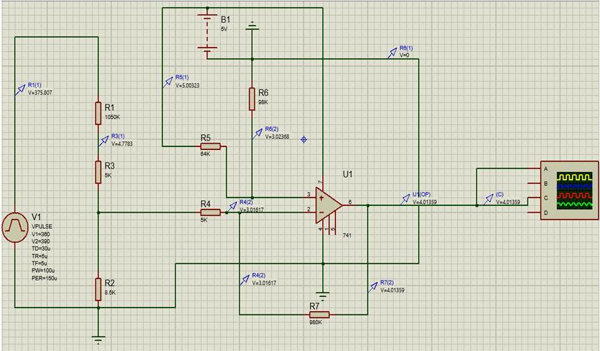
+VDC Comparator circuit is designed by using Operational amplifier to compare. The voltages in both control circuit and main circuit. It compares the voltage range of 320V to 400v. When the voltage range exceeds 365V in control circuit then we have to consider +VDC circuit Comparator triggers the output to the NAND gate. Similarly, when the voltage range exceeds 380V. When regenerative load condition then the main circuit triggers the output to the other NAND gate. This generally compares the output voltage which will be in the positive half cycle. This can be used in both the control circuit and the main circuit. The main objective of designing this circuit is to compare the two voltage ranges from the output and the regenerative load.


