4 minute read
Finishing first Atotech


FINISHING FIRST
Atotech is a global leader in the field of speciality chemicals for electronics and surface finishing. With an increased focus on semiconductor technology and electronics materials, the company continues to enhance its reputation as one of the world’s most innovative and successful chemical companies. Philip Yorke looks at the latest developments at Atotech and its strategy for future growth.
Atotech is one of the world’s leading suppliers of speciality chemicals, equipment, service and solutions for printed circuit board manufacturing and advanced electronics packaging. This is in addition to its expertise in both decorative and functional surface finishing. As well as its core business units, which include electronics and general metal finishing, other business units such as semiconductor technology and electronics materials are playing an increasingly important role in the future growth of the company.
Atotech was founded in 1993, when the Elf Atochem Group merged its M&T Halshaw operations with the Scheering electroplating division, which had a long history of electroplating dating back to 1901. Today Atotech is a direct subsidiary of Total, the world’s fifth largest oil and gas company, which was created from the merger of Total Fina and Elf Aquitaine in 2000.
Innovation driving sales
Atotech provides its customers with leading innovative technologies, which result from its intensive research and development programmes. In order to stay one step ahead of its competitors Atotech places R&D at the top of its list of priorities and sees it as an essential tool in all of its strategic business activities. This focus on innovative technologies has helped drive sales at Atotech since it was founded.
Being at the forefront of the next generation of technology means it is essential for the company to invest heavily in scientific support studies of product and process development. It also means that Atotech needs to consistently upgrade and expand its already extensive R&D facilities in Berlin.
Alongside the world’s leading manufacturers and OEMs, the company operates a unique global R&D network, which co-develops new production concepts to further drive innovation. Atotech’s global R&D teams seek out new paths and set the benchmarks for the development of sustainable plating processes. The success of these commitments can be measured not only by the increase in sales, but also the increasing number of Atotech patents. The company maintains close partnerships with its OEM customers as well as its tier one and two manufacturers in addition to institutes, universities and other notable research bodies. Leading in sustainable technology
Atotech told Industry Europe that sustainability means combining environmental protection and social responsibility with economic success. Atotech supplies its customers with high quality services and products and constantly strives to offer the best solution for the specific requirements of its customers.
The primary goal of Atotech is to protect the environment, as well as end users, its staff and production workers in the industries that the company serves. To achieve these goals the company works intensively on developing green alternatives to the conventional processes and systems used in today’s advanced plating industries. Atotech’s target is not only to comply with today’s strict chemical regulations, but to raise the standards even higher with its selfimposed commitment in order to eliminate all hazardous chemicals from its product portfolio.
New processes
New challenges in the industry and new technical requirements, as well as cost and environmental regulations, require a constant search for alternative manufacturing solutions for the printed circuit board industry. Today Atotech is at the forefront of technologies that minimise waste and reduce the environmental impact of its manufacturing processes and materials. Atotechs answer to these challenges is a new direct Paladium surface finish process called PallaBond, with an optional gold layer. The PallaBond process allows the direct deposition of Palladium on copper, without the need to use nickel. Therefore PallaBond is ideal for key press, high-frequency, flexible PCB gold, aluminium and copper wire bonding applications.
This patented process provides superior solder-joint strength for leadfree and eutectic soldering and is compatible with many new-based materials and solder-mark types owing to its short deposit time and low temperature requirements. In addition, the PallaBond process operates at a thickness of less than 300 nanometres, which is ideal for very fine lines and spaces. However most importantly the latest PallaBond process is free of toxic or hazardous materials such as thiourea, lead and Nickel.
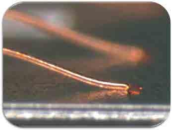
Pallabond is an environmentally friendly process, which has demonstrated outstanding technical advantages. It operates at higher yields and is enabling manufacturers to drastically reduce their operating costs compared top standard processes.
Future-proof processes
Atotech has an enviable reputation for its innovation-driven culture, which is designed to ‘future-proof’ the company with over 2000 worldwide patents currently in force. These have been developed at its 12 R&D centres worldwide, as the company continues to commit over 10 per cent of its annual sales to research and development. |This is to ensure that it will always have the most advanced, sustainable products and processes in its field.
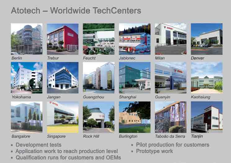
The regional headquarters of Atotech are located in Rock Hill (USA) and Yokohama (Japan) and are supported by over 40 regional service centres of which 18 are specialised technical centres that provide advanced analytical and technical support. With 14 production plants for chemistry and two for equipment, Atotech can be relied on to provide fast, on-time delivery worldwide. n
For further details of Atotech’s innovative products and services visit: www.atotech.com