6 minute read
MICRON SCHOOL OF MATERIALS SCIENCE AND ENGINEERING PROJECTS


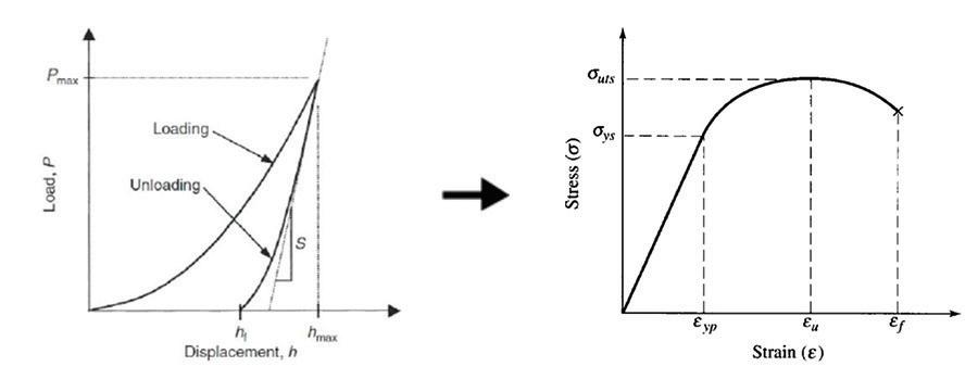
#52 – NANOINDENTATION OF THIN FILMS: FORCE-DISPLACEMENT TO STRESS-STRAIN
DEPARTMENT: Micron School of Material Science and Engineering TEAM MEMBERS: Ashton Enrriques Bette Gougar Carmen Wu CLIENT: Micron Technology PROJECT ADVISORS: Dr. Harold Ackler Dr. Paul Davis MENTORS: Dr. Paul Davis Dr. Steve Hues Thiagarajan Raman Derik Rudd Dr. Guohua Wei Nanoindentation is a mechanical indentation testing tool that is performed on small areas. This can provide information such as the hardness, young’s modulus, and other elastic properties of microscopic materials. However, nanoindentation does not provide information on materials as it transitions from elastic deformation to plastic deformation. This project seeks to accurately quantify the postelastic behavior of thin films by performing nanoindentation and developing a program that can convert these results into stress-strain curves. It is done by determining and validating a mathematical model with standards and then converting load-displacement data from nanoindentation into stress-strain curves.
#53 – DNA SEPARATION USING CUSTOM-BUILT MICROFLUIDIC DEVICE MICROFLUIDIC DESIGN AND DEVELOPMENT USING METHODS OF PHOTOLITHOGRAPHY
DEPARTMENT: Micron School of Material Science and Engineering TEAM MEMBERS: Hannah Byers Molly Graham Audrey Parker CLIENT: Micron School of Material Science and Engineering, Boise State Biology PROJECT ADVISORS: Dr. Harold Ackler Dr. Eric Hayden MENTORS: Dr. Paul Davis Travis Gabel Microfluidic devices capitalize on obtaining microscale chemical and physical properties of liquids and gasses. Composed of an array of channels and pathways, they are capable of directing, mixing, separating, and manipulating liquids for detailed analysis. Sponsored by Dr. Eric Hayden, assistant professor in the Boise State University Biology department, this project works to exploit microfluidic devices through the characterization and construction of microfluidic channels through methods of photolithography. The team has illustrated the methods for creating functioning microfluidic devices on campus which are capable of delivering known amounts of liquid to streamline DNA, RNA, and biological research.

#54 – CHARACTERIZATION OF “BLACK SPOTS” AND BULK MATERIAL DISCOLORATION IN LI3PO4 CERAMICS
DEPARTMENT: Micron School of Material Science and Engineering TEAM MEMBERS: Tommy Blank Cayden Doyle Quinn Hulse CLIENT: Tansmill Technologies Inc. PROJECT ADVISOR: Dr. Brian Jaques MENTOR: Dr. Henry Ji Li3PO4 ceramics serve as an effective sputtering target for the deposition of dielectric thin films in the semiconductor industry. However, macroscopic defects can form in the bulk of the material, including visible “black spots” and bulk material discoloration which is believed to occur during processing. Materials characterization techniques including x-ray diffraction (XRD), Raman spectroscopy (RMS), scanning electron microscopy (SEM), and electron backscatter diffraction (EBSD) can be used to determine possible causes for these macroscopic defects through microstructural and phase characterization. A combination of these techniques has revealed impurity phases to be present in the material and “black spot” regions to be highly porous. It is believed that impurity phases have led to a discoloration of the bulk material and powder agglomeration have created localized porous regions in the form of visible “black spots.” Characterizing these macroscopic defects can improve the processing and understanding of Li3PO4 ceramics which currently have little literature attributed to them.
#55 – COMPUTATIONAL MODELING OF CHEMICAL MECHANICAL PLANARIZATION BASED ON CONTACT MECHANICS
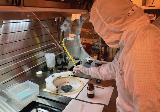
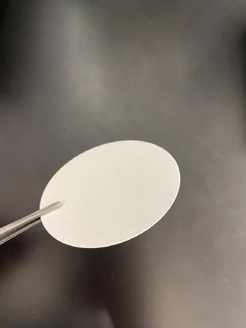
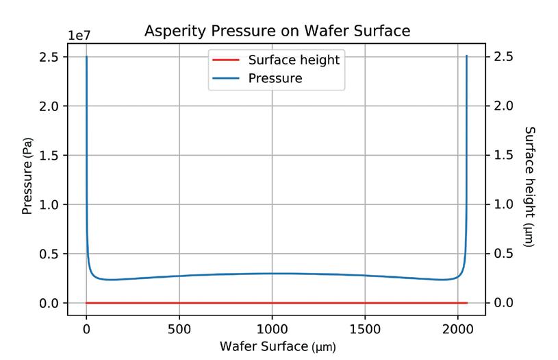
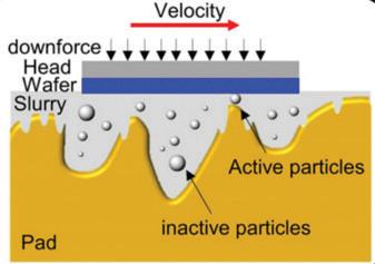
DEPARTMENT: Micron School of Material Science and Engineering TEAM MEMBERS: Josh Adams-Miller Emily Elliston Cade Greseth Cody LaCoursiere CLIENT: Micron Technology BSU MSMSE PROJECT ADVISOR: Dr. Harold Ackler MENTORS: Larecia Bercochear Jim Hofmann Dr. Steve Hues Dr. John Matovu Chemical Mechanical Planarization (CMP) is a critical process in the semiconductor industry that allows for precise and uniform patterning of thin films used to construct electrical devices. Wafers are polished on a CMP pad for a specified length of time to achieve surface planarity or to expose an underlying pattern of material. The types of materials used on the wafers, the shape of the patterns, and the size of the microscopic contact points of the CMP pad have a large influence on the planar uniformity of the surface after CMP. Micron Technology has sponsored some Boise State Univerisity MSMSE students to try and model the process using contact mechanics. The idea is to model the contact points of the CMP pad as elastic semi-spheres or cylinders. The pressure exerted on the wafer by these points can be calculated in the simulation. This pressure can then be plugged into the Preston’s equation to predict how much material is going to be removed. The model needs to be validated and evaluated based on real life data from CMP experiments. Upon validation the model can be used to predict the topography of wafers with adjusted parameters and materials alongwith different CMP pads and slurries. Therefore accomplishing the goal of the sponsors to reduce their resources spent trying to optimize their CMP process for each new part type.
DEPARTMENT: Micron School of Material Science and Engineering TEAM MEMBERS: Shannon Crain Jerry Murphy Dustin Nguyen CLIENT: Micron Technology PROJECT ADVISOR: Dr. Steve Hues MENTORS: Leticia Vazquez Bengochea Jim Hofmann Dr. Cody Johnson Dr. Guohau Wei The sponsor of this project, Micron Technology, Inc., is interested in learning more about the impact of the chemical mechanical planarization (CMP) process used on their semiconductor wafers. CMP is the process of polishing the surface of semiconductor wafers using a chemical slurry and mechanical grinding to obtain a smooth and flat surface (planarization). This process allows manufacturers to build 3D designs on their chips, for complex and powerful circuits. Any defects present on the planarized surface will cause imperfections on the additional layers, which can potentially cause the wafer to malfunction and become inoperable. The conditions that impact the CMP process are the nanoparticles used in the slurry, pressure placed on the wafers when polished, the roughness of the polishing pad, and the amount of time it is polished. The research is split into two teams, computational and experimental, and this team focuses on the experimental portion. The team is tasked with characterizing different CMP conditions and comparing the defects generated of each condition. The results from this team are shared with the computational team to help them with their modeling.
#57 – GARBAGE TO JUNK: 3D PRINT RECYCLING WITH PLA
DEPARTMENT: Micron School of Material Science and Engineering TEAM MEMBERS: Katie Bleffert Kelli Lucas Dylan Melander Hayes Neukom Laura Velvick CLIENT: Dr. Amy Moll Micron School of Material Science and Engineering PROJECT ADVISOR: Dr. Scott Phillips MENTOR: Dr. Amy Moll The process of 3D printing, frequently used in the Boise State student engineering shop and maker lab, can create waste prints that have either failed or are no longer needed. Within the larger scope of plastics recycling, this presents an opportunity for Boise State to recycle plastic in a closed loop system. Specifically, this project focuses on the recycling of PLA, a commonly used plastic for 3D printing. In this project a system was developed to process 3D print scraps into new usable filament. This recycled filament was characterized for its properties and performance comparative to commercial filament.


