6 minute read
FEATURE: RMIT’s Micro Nano Research Facility
Source: Sally Wood
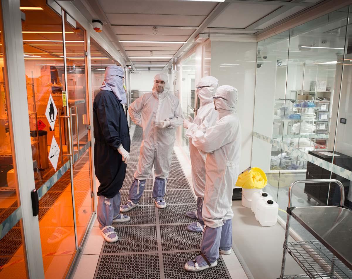
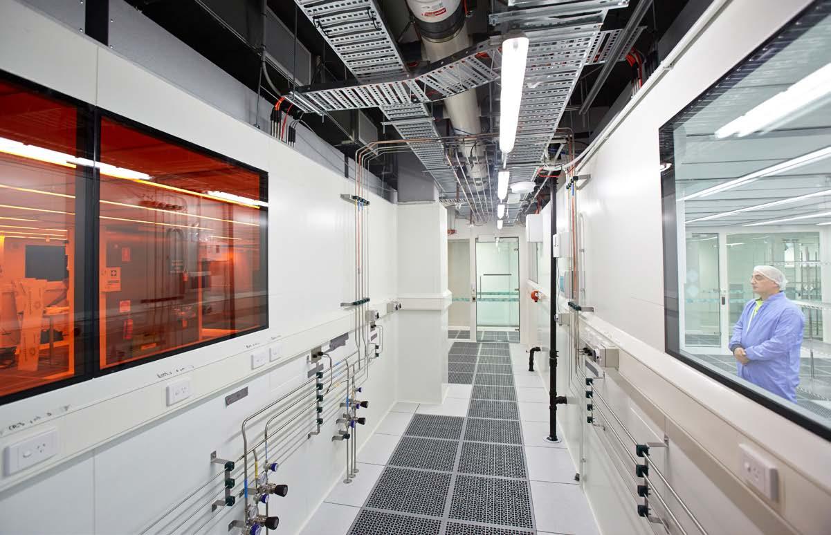
RMIT is home to the Micro Nano Research Facility (MNRF), where extensive nanotechnology research is undertaken. The MNRF, which houses nine laboratories, facilitates the design, modelling, fabrication, packaging and characterisation of micro and nano devices.
RMIT’s nanotechnology research embraces the interdisciplinary nature of the field and, as such, the MNRF is characterised by its ability to bring together a diverse range of high-quality micro and nano technology into a single facility.
Micro Nanomedical Research Centre
One of the key groups working within the MRNF are the researchers at RMIT’s Micro and Nanomedical Research Centre. Much of the work done at this Centre incorporates miniaturisation, which uses novel physics and engineering to miniaturise laboratoryscale processes and conventional medical procedures and protocols onto chip-scale devices, which can be integrated to form state-of-the-art medical technology. Their research aims to address some of the most pressing problems regarding current health technology. Furthermore, RMIT researchers in the micro and nanomedicine field operate within the framework of aiming to improve the availability, accessibility and affordability of point-of-care diagnostics, drug delivery, and biosensors. This could ultimately help to revolutionise the public health sector by providing medical practitioners and healthcare workers with the necessary advanced equipment for the early diagnosis, prognosis and treatment of preventable diseases. The three key themes of the Micro and Nanomedical Research Centre are: acoustically driven microfluids for biotechnological applications, including diagnostics and biosensing; phononic and photonic nanostructures for enhanced biomolecular detection; and inhaled gene and nanomedicine therapeutics. The applied research of the Micro and Nanomedical Research Centre has resulted in significant development of completely integrated low-cost portable devices for drug delivery and ultra-sensitive chemical detection, which are some of the smallest available on the market. One of the potential uses for devices such as these for providing new techniques and avenues for roadside testing of illicit drugs.
The team at the Micro and Nanomedical Research Centre are currently performing trials to test and demonstrate the of inhaled delivery of next generation therapeutics such as peptides, monoclonal antibodies, and siRNA, which could prove to be effective for a wide range of pulmonary diseases.
Nano-Earthquakes
In the area of ‘nano-earthquakes’, RMIT University’s Dr Sumeet Walia and Dr Amgad Rezk have examined the use of sound waves to controllably change the electronic properties of 2D materials, in a study led by Dr Sharath Sriram. The finding has important implications for electronics and optoelectronic devices made from 2D materials, opening the door to a new era of highly efficient solar cells and smart windows. Other possible fields of applications could include consumer imaging sensors suitable for low-light photography, for example in mobile phone cameras, which currently suffer from poor low-light performance, or in sensors for fluorescence imaging. Walia, from RMIT’s Functional Materials and Microsystems (FMM) Research Group, said atomically thin semiconductors, popularly called two-dimensional (2D) materials, had been known for decades, but their properties were a relatively new and exciting area for nanotechnology, with many promising applications in nanoelectronics and optoelectronics. Optoelectronic devices are electronic devices that can interact with, as well as control, light. This property can be harnessed for producing ultrasensitive detectors of light and high-speed phototransistors. The RMIT research looked at ways of using surface acoustic waves or ‘nanoearthquakes’ to control the properties of 2D materials. “Sound waves can be likened to ripples created on the surface of water, but where we can control the direction and intensity of these ripples,” Walia, a Research Fellow in the School of Electrical and Computer Engineering, said. “In this work, we use these ripples which occur on a crystal surface and couple it into
a material that is a few atomic layers thick (2D material), which causes a change in its electronic properties. “As the surface acoustic waves are turned on and off or increased and decreased in intensity, the change in electronic properties of the 2D materials follows the same pattern.” Rezk, a member of RMIT’s Micro and Nano Physics Research Laboratory (MNRL) and a Research Fellow in the School of Civil, Environmental and Chemical Engineering, said, “A simple technique to control these properties without affecting their inherent chemical and physical characteristics has been a primary scientific hurdle that has hindered their transformation into commercial products. “We’ve found that ‘nano-earthquake’- like waves under the surface of the 2D materials drag electrons along their path, thereby tuning the amount of light emitted by the material.” “Remarkably, the acoustic wave based tunability did not result in any structural or compositional change in the material.” “As soon as the acoustic waves were removed, the material retracted back to its initial optical state, and therefore this mechanism is highly adaptable for a variety of dynamically operating systems.”
Metal-Organic Frameworks
Researchers from RMIT have demonstrated a clean, green technique that can produce a customised metal-organic framework, or MOF, in minutes. MOFs are incredibly versatile and super porous nanomaterials that can be used to store, separate, release or protect almost anything. Predicted to be the defining material of the 21st century, MOFs are ideal for sensing and trapping substances at minute concentrations, to purify water or air, and can also hold large amounts of energy, for making better batteries and energy storage devices. Scientists have designed more than 88,000 precisely customised MOFs ¬– with applications ranging from agriculture to pharmaceuticals – but the traditional process for creating them is environmentally unsustainable and can take several hours or even days. Dr Heba Ahmed, a postdoctoral researcher in RMIT’s Micro and Nanophysics Research Laboratory, said the efficient and scalable

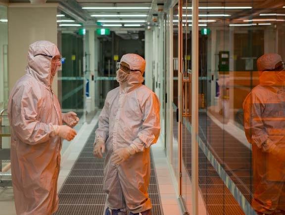
RMIT University’s Micro Nano Research Facility. Image credit: RMIT University.
method harnessed the precision power of high-frequency sound waves. “MOFs have boundless potential, but we need cleaner and faster synthesis techniques to take full advantage of all their possible benefits,” Ahmed said. “Our acoustically-driven approach avoids the environmental harms of traditional methods and produces ready-to-use MOFs quickly and sustainably.” “The technique not only eliminates one of the most time-consuming steps in making MOFs, it leaves no trace and can be easily scaled up for efficient mass production.” Metal-organic frameworks are crystalline powders full of tiny, molecular-sized holes. They have a unique structure – metals joined to each other by organic linkers – and are so porous that if you took a gram of a MOF and spread out its internal surface area, you would cover an area larger than a football pitch. During the standard production process, solvents and other contaminants become trapped in the MOF’s holes. To flush them out, scientists use a combination of vacuum and high temperatures or harmful chemical solvents in a process called “activation”. In their novel technique, RMIT researchers used a microchip to produce high-frequency sound waves. The ‘ingredients’ of a MOF – a metal precursor and a binding organic molecule – were exposed to sound waves produced by the microchip.


Using the sound waves to arrange and link these elements together, the researchers were able to create a highly ordered and porous network, while simultaneously ‘activating’ the MOF by pushing out the solvents from the holes.
Lead investigator, Distinguished Professor Leslie Yeo, said the new method produces MOFs with empty holes and a high surface area, eliminating the need for postsynthesis ‘activation’. The researchers successfully tested the approach on copper and iron-based MOFs, with the technique able to be expanded to other MOFs and scaled out for efficient green production of these smart materials.


