7 minute read
FEATURE: Melbourne Centre for Nanofabrication Feature
Source: Sally Wood
The Melbourne Centre for Nanofabrication (MCN) combines cutting-edge technology with the skills and experience of expert process engineers to form a world-class nanofabrication centre. MCN is a joint venture that functions in collaboration with six Victorian Universities (Monash University, Deakin University, The University of Melbourne, RMIT, La Trobe University, Swinburne University and Victoria University) and the CSIRO. MCN represents a $50+ million investment in micronanotechnology infrastructure.
MCN is proud to be part of the Australian National Fabrication Facility (ANFF), and is the largest and broadest capability within the ANFF network. Being a node of the ANFF enables MCN to connect with other national research facilities in micro and nanofabrication, allowing for the identification of partners, collaboration and innovation. MCN provides a pipeline for the design, fabrication, characterisation and testing of nanotechnology materials and devices at a single facility, which enhances productivity and quality gains for users. As such, MCN enables smooth transition from concept to prototype, while also offering the possibility to scale up to trial batch production, which creates a comprehensive user experience. By providing cutting-edge facilities and end-to-end services, MCN aims to be a world leader for the development and realisation of breakthrough technologies that harness nano and microfabrication.
MCN Services
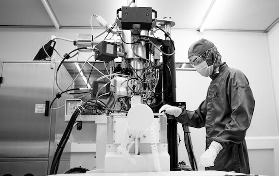
MCN is home to class 10,000 and class 100 clean room spaces, state-of-theart instrumentation, reconfigurable biochemistry and PC2 laboratories, and a world-class microscopy laboratory. These facilities enable MCN to provide services in key areas, including:
Lithography
MCN offers a wide range of lithographic techniques and instruments, including:

Electron beam lithography Hot embossing Nano imprint lithography Thermal scanning probe lithography PDMS soft lithography Direct write lithography Photolithography Spin coating and wafer development
Thin Film Deposition
MCN offers a wide array of techniques and instruments for thin film deposition, including: - Atomic layer deposition - E-Beam evaporation - Thermal evaporation - Diamond deposition - Chemical vapour deposition - Polymer electronics glovebox - Sputtering - Electroplating - Furnace systems for oxide and nitride growth
Characterisation
MCN features a broad range of instruments for the characterisation and imaging phase of fabrication processes, including: - Atomic force microscopy - Scanning electron microscopy - Spectroscopic ellipsometry - Laser doppler vibrometry - Profilometry - Laser scanning confocal microscopy - Laser TIRF - Microspectrometry - Hyperspectral imaging
Packaging
MCN provides the necessary equipment required for wafer bonding, dicing and wire bonding, which is necessary for the completion of most nano and microfabrication devices.
Etching
MCN houses two Reactive Ion Etching (RIE) systems, which are used extensively in the fields of LEDs, semiconductors, electronics, MEMs, communication technology, microfluids, optoelectronics, and photovoltaics.
Case Studies
A vast array of research is currently being undertaken at MCN in multiple fields. Some of these projects include:
Colour Coded Chemicals Researchers at La Trobe University, in collaboration with RMIT, have been investigating novel ways to analyse chemicals using visible light. This research has been facilitated by MCN’s facilities. The device they have developed uses the interactions between photons and electrons to filter out colours to create an ‘optical barcode’ that is unique to a sample and can be compared to a library of known material signatures. The tuneable and potentially portable device can help to quickly identify concentrations of chemicals and can be used for a variety of sensing applications, such as monitoring water pollutants and inspecting soil quality. The device does not chemically change or modify the solution being analysed, which means that it has the potential to be used for real-time monitoring, allowing for applications in food and pharmaceutical production industries. The device uses microfluidic channels to direct a liquid sample over a silver coating. Light is able to pass through the device thanks to an array of nanometresized holes that feature on the coating. Broadband light is passed through the liquid and is observed from the other side, enabling the identification of a sample. As it passes through the liquid and the array, all but one colour is filtered out, depending on the refractive index of the sample.
Superconducting Diamond
With the help of MCN’s facilities, a Victorian team of researchers has, for the first time in Australia, created superconducting diamond. Diamonds are an exceptional natural material. They are the hardest naturally occurring substance, they don’t corrode, and they are an incredible thermal conductor. By adding superconductivity to diamond’s list of characteristics offers exciting prospects for a novel class of highly robust devices. Additionally, superconducting diamond represents a step towards a material that exhibits absolutely no electrical resistance at room temperature, which would be a ground-breaking development in the realm of materials science. Professor Marvin Cohen, an award-winning theorist from the University of California at Berkeley, believes that diamond could be the material to make this achievement possible.
However, producing superconductivity in a diamond at any diamond has proved to be incredibly difficult, with only a few labs around the world achieving it. A team from the University of Melbourne have joined the elite few who have been successful in doing so. Their research showed that, by adding a dose of boron – a process known as doping – diamond shows superconducting properties at temperatures around 2K. Using MCN’s diamond chemical vapour deposition capabilities, the team were able to introduce boron which diamond is being grown.

Nanolenses MCN has played a critical role in providing a team of researchers with the facilities required to enable their creation of a scalable production method for a class of nanoscale lenses using the electrostatic forces between charged nanoparticles, enabling wider application of the technology. Using the gaps between triplets – or trimers – of different sized nanoparticles, these nanolenses are able to focus light. Thanks to their miniscule size and very highyield enhancement, they show an enormous amount of promise in a range of optical and sensing applications. The main thing currently limiting their widespread uptake is their expensive and laborious production process. Dr Julian Lloyd, lead author of the research, and his colleagues’ method employs induced electrostatic forces to self-assemble the gold nanoparticle triplets. This method enables these trimers to be produced with a more than 60% yield – which are unprecedented quantities. Moreover, it removes the need for expensive ‘top-down’ fabrication techniques that have traditionally been used, and which limit the fabrication process’s scalability. In their research, the team placed differing surface charges on the nanoparticles, which enabled the structures to dram themselves into place.
Back-Contacted Solar Cells
Solar cells are an incredibly promising technology that can help to reduce Australia’s carbon footprint. However, current technologies’ inefficiencies prevent widespread use. However, a team of researchers working out of MCN have combined the benefits of back-contacted silicone cells and perovskite materials, which offers the possibility for the development of more efficient photovoltaic devices. The researchers were able to combine the benefits of both back-contacted silicone cells and perovskite-based devices by using a series of photolithography and vacuum deposition processes. Until now, the combining of a back-contacted design to the perovskite solar cell has proven incredibly difficult because the interdigitated array of electrodes must be delicately structured, which provides a number of major challenges for fabrication. This novel process, however, enables an alternative design in which the interlocking array of anodes and cathodes are no longer on the same plane, but remain only on one side of the perovskite absorber layer. As a result, the research has, for the first time, demonstrated the possibility of constructing a back-contacted PSC. While the design is less efficient than what can currently be achieved in conventional siliconbased designs, once optimised these new cells have the potential to provide far higher conversion rates.
Speeding Up Solar Cell Development
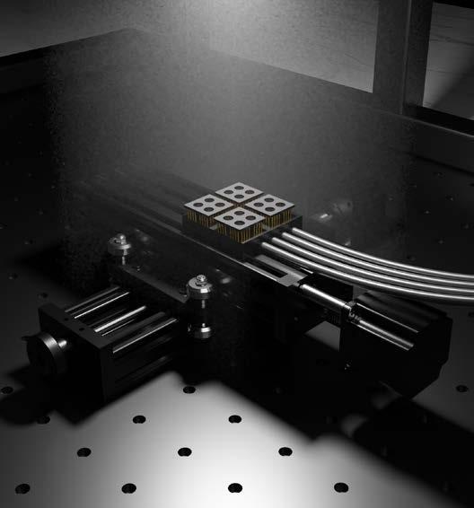
Tests on new designs for perovskite solar cells can now be conducted in minutes instead of days, thanks to a new system built by PhD candidate Adam Surmiak from the ARC Centre of Excellence in Exciton Science (Exciton Science) and his colleagues based at Monash University. The invention means that the performance and commercial potential of new compounds can be rapidly evaluated, significantly speeding up the development process. The machine, known as a ‘16-channel parallel characterisation system’, can analyse sample perovskite-based solar cells in just 10 to 15 minutes. Essential to the system’s operation is a series of 3D-printed components that were fabricated with micrometre precision at the Melbourne Centre for Nanofabrication, part of the Australian National Fabrication Facility’s Victorian Node. Alongside the development and set-up of this new testing facility, Surmiak and the team were also able to significantly speed up the actual solar cell fabrication process. The head of the Monash University lab in which Surmiak works, Professor Udo Bach, a chief investigator with Exciton Science, described the invention as world-leading. “Our new set-up has the capacity to test thousands of solar cells in one single day, putting us ahead of practically all other R&D labs worldwide,” Professor Bach said.
A detail from the new 16-channel parallel characterisation system. Credit: Adam Surmiak, Xiongfeng Lin.


