29 minute read
037
Frequency ranges Class 1 Class 2 Class 3
Hz Test levels % U1 Test levels % U1 Test levels % U1
Advertisement
16 – 100 - 2.5 4
100 – 500 -
500 – 750 5 9 3.5 5
750 – 1 000 -
1 000 – 2 000 2 3 1.5 2
Class definition is the same as that described in section 3.7. The compatibility and immunity levels must obviously be higher. The reference standards for this are IEC 61000-2-2 for low voltage public power supply systems and IEC 61000-2-4 for nonpublic industrial plants. One of the parameters defined in the two standards mentioned above is Total Harmonic Distorsion (THD), equal to the sum of the r.m.s. values of harmonic components Qh up to a certain order H, generally 40, divided by the r.m.s. value of fundamental Q1. For example, the THD value of the three classes whose waveform is illustrated in figure 25 is 12% for class 1, 17% for class 2 and 27% for class 3. By way of reference, standard EN 50160, which defines the characteristics of the voltage supplied by the public networks, establishes that the THD value in medium voltage must not be more than 8%.
— 4. Effects and control of interference
4.1 Effects of electromagnetic disturbance
The effects of electromagnetic disturbance on an apparatus due to a coupling, called interference, can range from simple functional disturbance to destruction of one of its parts resulting in total loss of its functionality. The standard envisages three criteria regarding the performance of equipment (EUT, Equipment Under Test) subjected to an electromagnetic compatibility test (EN 61000-6-2 Part 6-2: Generic standards - Immunity standard for industrial environments. • criterion A: The EUT continues to function as envisaged during and after the test without degradation of performance or loss of functionality below the performance level specified by the manufacturer; • criterion B: The EUT continues to function as envisaged after the test without degradation of performance or loss of functionality below the performance level specified by the manufacturer;
However, performance degradation is allowed during the test, but not changes in the actual operating status or the stored data; • criterion C: temporary loss of functionality during the test is allowed. However, functionality is auto-recoverable or can be, by means of a manual command imparted by the user. Generally speaking, if the EUT becomes dangerous after the tests, it is considered to have failed the actual tests themselves. Electrical equipment must be immune to both high and low frequency phenomena. High frequency phenomena include the already described electrostatic discharge (ESD), radiated electromagnetic fields, electrical fast transients/ bursts (EFT/BURST), disturbances caused by conducted electromagnetic fields and voltage pulses (SURGE). The more typical low voltage phenomena include harmonics, voltage dips, micro-interruptions and voltage unbalance. However, it is important to underscore that the tests do not cover all the possible combinations of negative factors present in real situations.
4.2 How to deal with electromagnetic incompatibility
The process for dealing with EMC problems can be addressed in two different ways, depending on the moment in which they are faced. The first approach, basically to be adopted during the design stage, is to assign a level of compatibility with each disturbance, to the environment in which the equipment will be installed (fig. 26). A general suppression pattern can then be defined, after which the emission and immunity levels of all the equipment to be installed can be specified along with the relative suppression and installation methods. This approach is certainly the best if it can, in fact, be applied. A new installation with a single design engineer who has a general view of everything and who can then issue a document of EMC requirements is a typical example. The steps to be followed are illustrated below:
Figure 26: process to adopt beginning with design engineering

Figure 27: process to adopt for existing installations
The second approach (fig. 27) is adopted in existing installations when apparatus must be installed for which the EMC characteristics cannot be changed. In this case, an attempt must be made to match the existing compatibility level of the installation with the levels of the components that must be installed. This can only be achieved by adopting methods to mitigate the disturbances that affect the the new apparatus. This second approach is certainly more complicated and requires the assistance of an experienced EMC specialist who must be preferably called in before the apparatuses are installed but who often has to resolve problems which arise after installation. The steps to take are outlined in fig. 27.
4.3 Methods for controling interference
As explained in the previous section, the essential thing is to define disturbance mitigation methods both when new installations are designed and when existing installations are enlarged. In a nutshell, all methods are based on reducing the degree of coupling through which disturbance interferes with the electronic receiver apparatus. This is particularly true of high frequency signals, in which the interfering signals and wanted signals are in the same frequency range. Various different methods for mitigating interference in relation to the type of disturbance coupling are analyzed in the following pages.
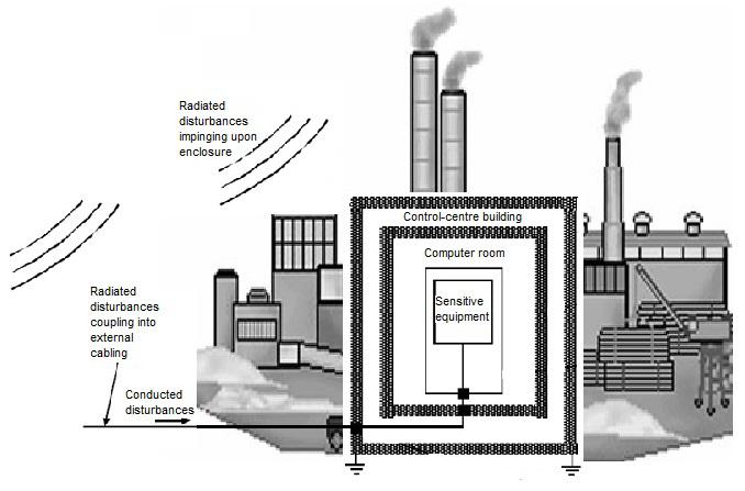
Figure 28: EMC for an industrial control center
— 4. Effects and control of interference
4.3.1 Methods for mitigating conducted disturbances
Conducted disturbances can propagate to other apparatuses through all conductive components, including cables, earthing systems and the metal frameworks of switchgear.
4.3.1.1 Circuit balancing
Circuit balancing is the first rule to consider. In an unbalanced circuit, the summation of the currents in the main conductors is different from zero, thus there is a common mode current that is different from zero. It can be demonstrated that, since the signal propagates by means of a residual current, it is important for the circuit to be balanced in order to be immune from conducted disturbance. In this situation, the signal associated with the residual current will be different from zero and immune to the disturbance, which propagates in the common mode.
4.3.1.2 Chokes
The second method is to wind the conductors around rings of ferromagnetic substance (nornally ferrite) with coils in phase opposition (to allow the supply currents of the device – which are in the differential mode but at much lower frequencies than those concerning EMI - to generate flows that cancel each other out) so as to create so-called chokes (fig. 29). The coil introduces an impedance, which is maximum for common mode currents and therefore limits the disturbance, and minimum for the differential mode currents pertaining to the signal.

Figure 29: circuit with choke
Ferrite is normally used to prevent saturation at high frequencies.
4.3.1.3 Filters
Another method is to install filters. Low-pass, high-pass, band-pass and band-stop filters can be used. For the purpose of preventing disturbance, the components must be installed in series with the circuit, as in the following cases (fig. 30):
The components, basically the capacitors, must be installed in parallel as in the next case (fig. 31) if the disturbances are to be discharged to earth:
To eliminate high frequency disturbances, the filters used normally consist of inductances in series and capacitance in parallel. There are the following types: • feedthrough capacitor type filter (fig. 32): used when the impedances of the generator and receiver are relatively high;
• half T or L filter (fig. 33): the inductance must be positioned on the low impedance side and is used when the impedance of the generator is much different from the impedance of the receiver;
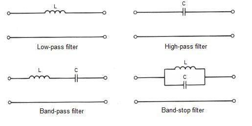
Figure 30: filters in series
Figure 31: filters in parallel
Figure 32: feedthrough capacitor type filter

Figure 33: half T filters
• the π type filter (fig. 34) , used in high impedance circuits;
Figure 34: π type filter
• the T type filter (fig. 35) is used in circuits where the impedances of the generator and load are relatively small.
4.3.1.4 Varistors
Varistors belong to the family of suppression devices used as a protection against overvoltage. Variators are nonlinear resistors, the resistance of which depends on the voltage applied. This can change from MΩ to mΩ values in a few nanoseconds (typical values from 10ns ... 25ns) and can tolerate current up to 25kA and energy up to 600kJ. These devices possess 100pF to 10nF parasitic capacitance, which can limit the protected signal band but which also contributes towards filtering disturbances. Since the performance of a varistor depends on its temperature, it is important to prevent it from being heated or, simply, to keep it away from hot spots. Figure 36 illustrates the typical curve of a zinc oxide varistor (MOV). It is advisable to make sure that residual voltage Ures at I max current value is never more than the withstand voltage of the apparatus being protected. In addition, figure 37 shows how the current peak associated with the pulse and that the varistor is able to support increases as pulse duration and number of pulses decrease. Thus the disturbance must be appropriately defined as to pulse number and duration, thereby allowing the component to be chosen on the basis of the maximum supportable power and energy.
4.3.1.5 Suppression diodes
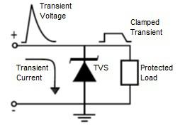
Suppression diodes (transils) also maintain voltage at a constant level on the load in the presence of overvoltage but, compared to varistors, cannot conduct high currents and therefore support reduced amounts of energy. On the other hand, they are very fast with response times in the picosecond range.
Figure 35: T filter
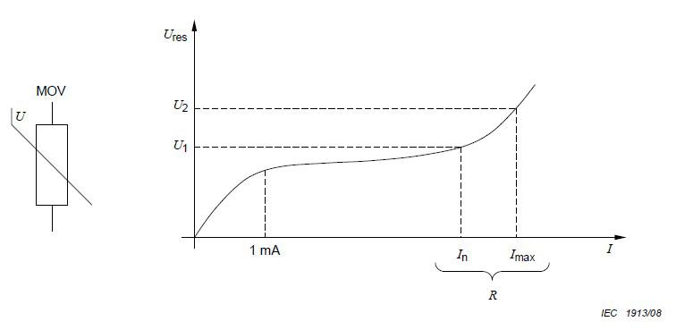
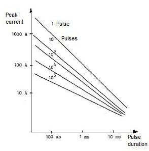
Figure 37: curves of the current peak supported by a varistor
— 4. Effects and control of interference
To select the right transil it is important to first define the rated voltage of the circuit in which the components will be installed. In addition: • make sure that the transient peak current of the disturbance is less than the peak value of the rated current pulse corresponding to clamping voltage Vcl; • check Transil average power dissipation PAV, especially when there is repeated disturbance.
Given energy W of the individual disturbance and frequency f of the disturbances, the energy of the individual disturbance is calculated using the formula PAV = f*W; • make sure that the circuit can support clamping voltage Vcl (i.e. the voltage present when the
Transil conducts its fully rated current); • to reduce leakage current, make sure that the rated voltage is far from the clamping voltage.
4.3.1.6 Noise suppression devices
Noise suppression devices, or spike killers (fig. 39), are ferrites formed by amorphous material inserted into the terminals of the devices themselves. They function in a different way from conventional filters since their task is to reduce disturbance at its origin, when the source of disturbance is generated by rapid voltage and current changes (ringing or reverse recovery of diodes, etc.). Amorphous cores eliminate these disturbances regardless of the frequency.
Figure 39: spike killers
4.3.1.7 Positions of filters and protections
The filters and protections described in the previous sections must be installed correctly, otherwise their performance will be impaired. As established by the classification provided by standard IEC 61000-5-1, there are two types of approach to protection, global and distributed. As illustrated in figure 40, global protection is obtained with a single barrier, where the protection must protect the entire installation and must therefore be installed at the point of access to the shielded environment. It would be wrong to install the protection inside the shield since this would allow disturbances to enter the environment. There must obviously be no internal sources of disturbance.
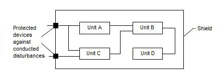
Figure 40: global protection system with single barrier
If there are apparatuses with different levels of immunity, the environment can be divided by cascaded barriers (fig. 41).
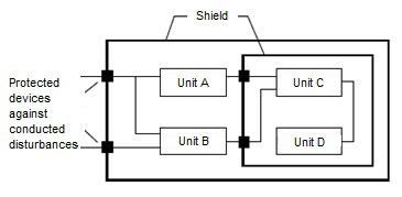
Figure 41: multiple barrier global protection system
The protections in distributed protection systems (fig. 42) are installed on each individual apparatus without a sufficient immunity level.
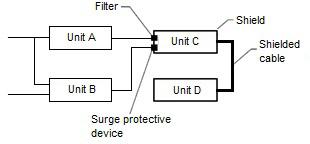
4.3.2 Methods for mitigating radiated disturbances 4.3.2.1 Shielding
Shielding of an apparatus increases its immunity to external electromagnetic fields and reduces emissions into the outside environment. Shielding can be extended to an entire environment containing a group of apparatuses, such as a test laboratory. The following paragraphs describe what takes place when an incident electromagnetic field passes through a shield.
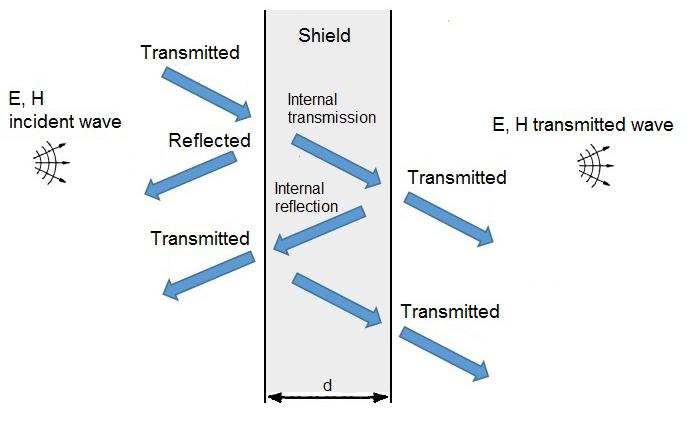
Figure 43: transmission of electromagnetic disturbances in a shield
As shown in figure 43, the electromagnetic field transmitted beyond the shield will equal the incident field minus the losses due to reflection R, absorption A and multiple reflections M. Shielding Effectiveness (SE) is expressed as:
or in decibels as:
Based on the calculations above, the efficiency of a shield will thus be given by:
where RdB is the coefficient of reflection, AdB is the absorption coefficient and MdB is the coefficient of multiple reflections. Considering δ as the depth of penetration of the electromagnetic field, this depends on the frequency f, permeability µ and conductivity σ of the material according to the following formula:

Thus the depth of penetration decreases as the frequency increases and the shielding characteristics of the material (such as permeability and conductivity) improve. For example, the penetration depth of copper at 60 Hz is 8.5 mm but becomes just 0.02 mm at 10 MHz. If the thickness of the shield d exceeds the depth of penetration, the contribution provided by loss through absorption becomes significant since absorption coefficient A is:
In addition, if d>>δ, coefficient MdB (the value of which is negative since the reflections within the shield contribute towards increasing the transmitted field, therefore reducing shielding effectiveness) becomes negligible. For the far-field, thus plane wave incident perpendicular to the shield, reflection coefficient is where η is the impedance of the shield material and η0 = 376.7 Ω is the impedance of the air. This coefficient depends on the quality of the shield material and can range from 0 in the absence of a shield (η = η0) to 1 if η<< η0, thus of a material with excellent conductivity, such as metallic materials. By way of example, the following table lists the impedance η of certain materials used for shields:
Material
Aluminium
Mu-metal
Iron
η [Ω]
3.8 • 10-6
6.3 • 10-3
8.5 • 10-4
— 4. Effects and control of interference
In conclusion, one can affirm that in the presence of far-field electric and magnetic sources, loss by reflection is the predominant phenomenon at low frequencies while at high frequencies it is absorption (always so long as d>>δ). However, when it comes to near-field sources and while, in relation to the electric field, the shield behaves in exactly the same way as described above, its behaviour in relation to the magnetic field is different: loss by absorption is prevalent at all frequencies even though it is low at low frequencies. This means that alternative methods must be found to shield magnetic fields at low frequencies, such as use of low-reluctance materials. Materials which are both conductors and magnetic therefore give the best results, as shown in figure 44.
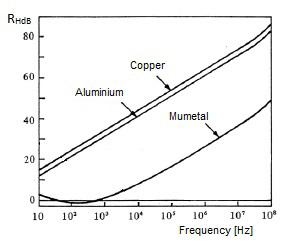
Figure 44: coefficient RHdB in relation to frequency for certain materials
When the previously described notions are applied, one can affirm that all apparatuses should be completely enclosed in housings made of suitable materials, typically metallic. Since the enclosures of electrical or electronic equipment are either made of metal or plastic, in the former case the enclosure is able to provide a shielding action while in the latter case, methods able to create characteristics that suit the materials used must be provided when necessary. When the enclosures are made, attention must be paid: • to the openings, sometimes indispensable when heat exchange with the outside is required; • to routing the feeder and signal cables that supply power to the apparatus and exchange data with the outside; • to any openable doors that might be present. Consult standard IEC 61936-1, Power installations exceeding 1 kV AC – Part 1: Common rules if the installation falls under this category.
The following are valid general rules: • reduce the number of openings to the minium.
When they are absolutely necessary and to obtain efficient shielding, it is good practice to ensure that length L of the openings in the enclosure does not exceed one tenth of the wavelength of the incident electromagnetic radiation. For example, 300 MHz test frequency corresponds to 1.00 m wavelength λ. This means that the length of the openings must not exceed λ/10, i.e. 100 mm. This is not a problem in individual apparatuses (see figure 45), but must be carefully considered for control cubicles.
Generally speaking, it is advisable to never have openings with diagonal measurements exceeding 100 mm while, in the presence of higher frequencies (e.g. 1 GHz), the openings should not exceed λ/10 = 30 mm.
Figure 45: openings in an IED (Intelligent Electronic Device)
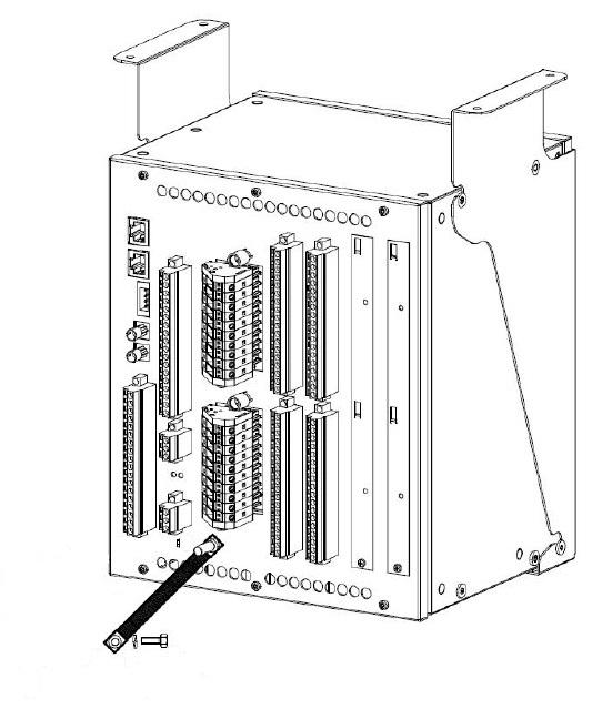
• when larger shielding enclosures (e.g. control cubicles) are assembled, a metal gasket must be inserted between the panels when they are joined together or in any case, they must have an unpainted anti-corrosion finish in all points of contact with other plates, etc. • use metal gaskets for openable doors and panels or connect them to the fixed structure by means of suitable conductors (fig.46);
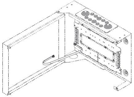
Figure 46: example of a connection between LV compartment and door
• the shields of the cables entering or leaving the enclosure must be connected to the enclosure itself and must be filtered. Analog signals from current transformers can be a strong source of disturbance in electric power panels. For this reason, these circuits must be routed in metal conduits, flexible metallic tubes or metallic braiding. These protections must reach right up to the low voltage compartment and must be earthed. The shields must must be as continuous as possible. They must also have a low resistance (a few ohms per kilometer) and a low coupling impedance in the disturbance frequency range.
The earth connection of the shields must be as short as possible and must affect both ends. A 360° connection is best. Obviously, the shields of the incoming cables must be earthed at their entrance into the panel to prevent coupling inside to unshielded circuits (fig. 47).
Use of conductive sleeves is another method (fig. 48): the sleeve must be connected to the Faraday cage by screwing it onto a specially designed collar in the cable gland plate.
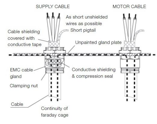
Figure 47: earthing with cable gland
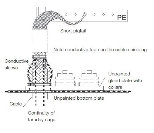
Figure 48: earthing with conductive sleeve
— 4. Effects and control of interference
Cable clamps can be used so long as they are earthed (fig. 49). In this case the cable glands are no longer necessary.
Figure 50 gives a concrete example of good practice where a shielded cable is connected in an enclosure represented by the plate: Lastly, the measures to apply in a control panel are outlined in figure 51.
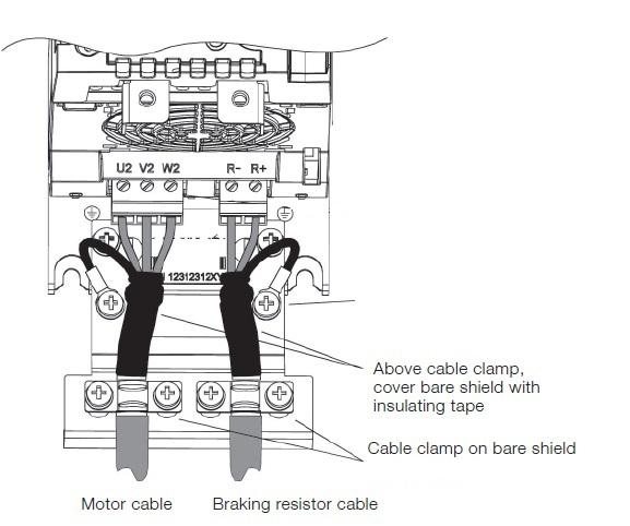
Figure 49: earthing with cable clamps
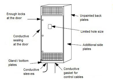
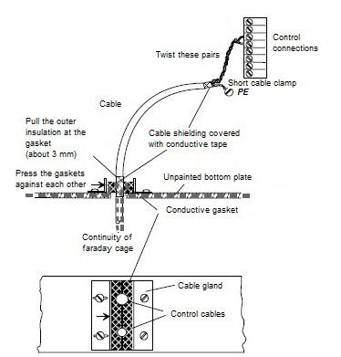
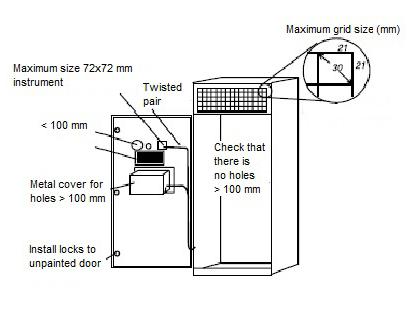
Figure 50: example of a correct connection Figure 51: outline of EMC measures in a control panel
4.3.2.2 Indications concerning cables
We will now consider a piece of conductor with diameter d and finite length and represent it with constants concentrated per unit length (fig. 52):
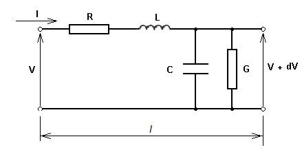
Figure 52: diagram of a conductor
Where R and L are the longitudinal resistance and inductance and C and G are the transversal capacitance and conductance for a unit length l of conductor. Besides increasing as the temperature rises, resistance R also increases as the frequency of the signal increases. This phenomenon is caused by the tendency of the current to concentrate on the surface of the conductor and is known as skin effect. The variation is proportional to the square root of the frequency of the signal, as in the formula below:
where k is a constant that depends on the type of conductor, with diameter d, and R0 is the D.C. resistivity.
Inductance takes account of the effect due to the magnetic field generated by the circulation of direct current through the conductor itself, i.e. of self-inductance, which we will call Li, and of that due to the presence of two conductors, i.e. to mutual inductance L e . Thus overall inductance can be calculated as sum L = Li + L e .
Since Li is inversely proportional to the diameter and to the root of the frequency, according to the following formula:
with L0=µ0/8π low frequency inductance and k’ a constant which depends on the type of conductor one can affirm that as the frequency increases, Li decreases while L e does not change since it depends on the distance between the conductors and their diameter. However, one must consider that Li is small in relation to L e, thus one can generally affirm that inductance varies little with frequency.
Capacitance C stands for the parassitic capacitance due to the difference in potential between the two conductors and is proportional to the dielectric constant of the insulation in between. In the case of a diameter d, distance D away from a surface (with D>1.25•d) there is: where k” is a constant and ɛ is the relative dielectric constant of the insulation. C is therefore dependant on the nature of the dielectric component and the geometry of the circuit.
Lastly, conductance G is due to the leakage current between the conductors, caused by imperfections in the insulation, and is normally negligible. Conductance is conditioned by the nature of the insulation in between, by the frequency of the signal and by the distance between conductors.
Now, considering impedance Z per unit length and given that:
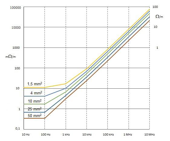
one can affirm that the cable has an impedance per unit length which varies depending on the frequency, in particular with a resistance proportional to the square root of the frequency and an almost constant inductance. The linear impedance trend in relation to frequency in certain sections of cable is illustrated in figure 53.
Figure 53: impedance in relation to frequency in certain cables
— 4. Effects and control of interference
Note that when the frequency rises, it is advisable to route several cables of smaller section in parallel rather than one single cable of a larger section. Certain conclusions can therefore be drawn concerning the behaviour of wiring in relation to disturbances: • the impedance of a cable increases as a function of length and frequency. Thus, in the case of high frequency disturbance, the earthing conductors must be as short as possible. Any excess length must be eliminated and the earth connection point must be as near as possible. For example, for apparatus in the low voltage compartment, it is important to connect to the nearest point of the metal structure of the switchgear (fig. 54). It is therefore important to avoid these two lengths as a funzione of the frequency of the disturbance emitted by the apparatus. Since the second case is the most realistic and bearing in mind that λ=c/f, the result is:
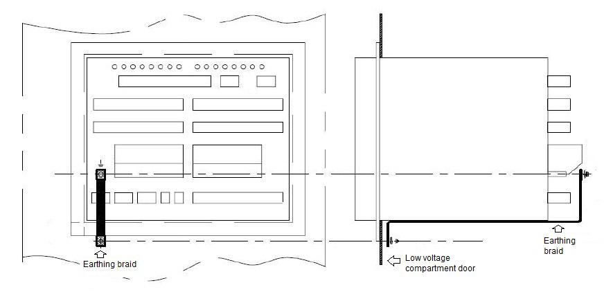
Figure 54: example of the earth connection of an IED
• since it represents possible points through which disturbance can enter, all internal wiring must be as short as possible. In addition, if the conductors are connected to apparatuses which are sources of disturbance inside the switchgear, they could act as antennas and emit radiated disturbance. There are two types of antenna: dipole (fig. 55a) and monopole (fig. 55b); the antenna effect occurs in conductor lengths l=λ/2 in the first case and l=λ/4 in the second case.
l
a) l/2
l/2 h
b)
For example, at a frequency of 80 MHz (one of the frequencies envisaged for the tests) l will equal about one meter. In such cases, it is therefore advisable to use cables of a shorter length; • cables of different classes should be routed separately. There are two classes of signals for receivers: - Class 1 signals, highly susceptible (e.g. signals produced by sensors, load cells, etc.); - Class 2 signals, susceptible (e.g. analog signal circuits); and two classes of signals for sources, i.e.: - Class 3 signals, disturbers (e.g. diode feeders, solenoid valves, etc.) - Class 4 signals, highly disturbing (e.g. power converters such as inverters and switching feeders, remote control switches, brush motors, etc.). To reduce the number of couplings, it is good practice, when possible, to route the cables near to metal parts connected to the reference potential (assembly plates, electric cabinet, etc.). It is also important to use cable trays, cable conduits or tubes made of metal (not plastic) for class 3 and 4 conductors (fig. 56).
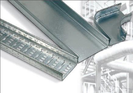
Figure 56: examples of metal cable trays
Figure 55: dipole antenna a) and monopole antenna b)
It is advisable for cables pertaining to different signal classes to follow different routes and be suitably spaced. The minimum distances, purely indicative, could be those given below:
Minimum distance in mm
Class 1 Class 2 Class 3
Class 1 Class 2 Class 3
Class 4
150 300 500 150 300 150
Keep to a 90° angle of intersection if cables in classes 1-2 and 3-4 should cross each other. If the distance between class 1 and class 4 cables is less than 1 m, the Standard recommends that the former be routed within closed metal conduit.
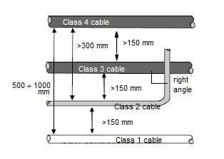
Figure 57: diagram of minimum distances between cables of different classes
• Use of twisted cable to prevent disturbance is common practice (fig. 58). Unshielded twisted pair cable (or UTP) consists of two insulated wires twisted together so as to reduce disturbance due to external electromagnetic fields. These latter induce currents in the coils that flow in opposite directions and tend to cancel themselves. This method is certainly advantageous since it is economical and flexible.
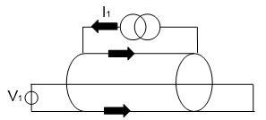
However, it is unable to completely eliminate disturbance, especially at frequencies of around 1 GHz. • Use of shielded cables. Shielded cables are efficacious for high frequency transmissions, for connections between measuring instruments and, generally speaking, for transmitting signals of weak intensity. On the other hand, they are more expensive, the cables are inflexible and the connections more complex. The model of a shielded cable is illustrated in figure 59:
A disturbance in current I1 flowing through the shield produces, as a consequence, a disturbance in voltage V1 given by:
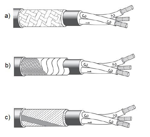
Since the ideal shield has a typical impedance ZT = 1...10 mΩ , it means that the shield contributes towards diminishing the disturbance by ZT times. The shield (fig. 60) normally consists of conductive mesh (a), a wound copper conductor (b) or aluminium foil wrapped in a helical or cigarette paper fashion (c) around the central conductors. Several mixed types of shields are used to reduce the effect of the openings in the mesh and achieve efficiency even at higher frequencies.
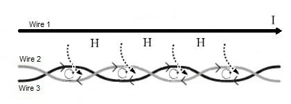
Figure 58: coupling diagram for twisted pair cable Figure 59: representative circuit for a shielded cable
— 4. Effects and control of interference
The disadvantage of these solutions is that they make cables more expensive and liable to be damaged by bending. In addition, oxidation could impair their continuity and, thus, their efficacy. The typical impedance in the case of continuous tubular shields depends on the geometric characteristics and material used, while admittance is null since the electric field does not penetrate through a continuous shield, which is without openings. In the case of mesh shields (fig. 61), the openings must be taken into account as well as the inevitable penetration of magnetic where Zd is the impedance of the tubular shield while termination M represents the mutual inductance due to the magnetic field having penetrated through the openings (r1 is the internal radius of the shield, L its length, P the mesh pitch and α the tilt angle).
The graph in figure 62 shows how the impedance of a cable (with respect to DC-resistance R0) with mesh shield coincides with that of a continuous shield until the width of the openings becomes comparable to the wavelength of the disturbance, after which the two curves diverge and the mesh shield begins to lose its efficacy. The shield must be connected at both ends, otherwise it could act as a waveguide or antenna.
lines of force through the openings themselves. The typical transfer impedance can be expressed as:
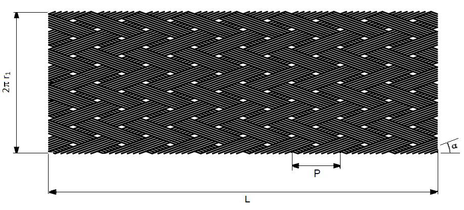
Figure 61: mesh shield
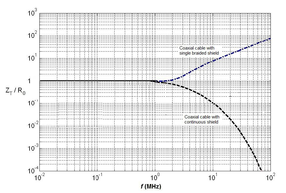
Figure 62: transfer impedance of a conductor with mesh shield and continuous shield
One of the reasons for earthing just one of the two ends is that should there be a significant difference in the voltage between the connection points at each end of the shield, the current that would pass through could also damage the cable. This difference in voltage is not unusual in large installations or in connections between buildings. However, the best solution is to improve the earthing network, e.g. by using a meshed network with an appropriate number of ground rods in parallel, and to maintain the shield protection by earthing both ends. In long sections, where the cable must be divided into several parts, conductive gaskets must be used for earthing the cable shields. A 360° connection is best, i.e. it must completely surround the shield in order to maintain an efficient shielding effect (fig. 63).
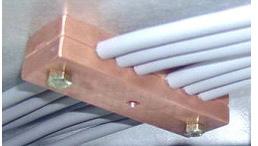
Figure 63: conductive joint
Since, as mentioned previously, the best way to shield radiated disturbances is to earth both ends of the shield, cables with double shielding can be used when it is impossible to prevent current from flowing into the shield. In this case, just one end of each individual shield can be earthed as shown in the diagram in figure 64: The model in figure 65 shows how the parassitic capacitances become distributed in the cable.
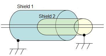
Capacitance C3 is actually a bridge for disturbances between shield 1 and shield 2 to earth (fig. 66)
The model for long cables at high frequencies is similar to that of the cable with single shield earthed at both ends. When it comes to protection against magnetic fields, the only solution is to encapsulate the parts that need to be protected in containers made of ferromagnetic substance with a higher magnetic permeability than air.
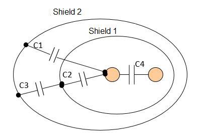
Figure 65: circuit of a cable with double shield
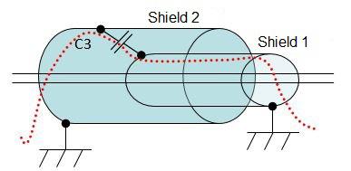
Figure 66: route taken by disturbance in a cable with double shield
Figure 64: earthing of a cable with double shield
— 4. Effects and control of interference
4.3.3 Protective earth and earth (functional)
First a brief outline to describe what is meant by protective earth and earth (functional). From the electrical viewpoint, earth is ground which conventionally has 0 V reference potential. Protective earth refers to one or more points in a system or installation that are intended for electrical safety purposes while, by exclusion, functional earth refers to one or more points that are not intended for safety purposes. The electrical symbols are illustrated in figure 67:
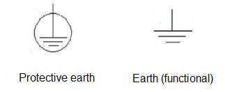
Figure 67: earth symbols
Thus earthing comprises elements able to bring a conductor to earth potential.
Earth must not be confused with a mass, frame or chassis which is a conductive point or element that constitutes the reference potential of an apparatus or a circuit and which may or may not be earthed. The reference symbol in this case is illustrated in figure 68:
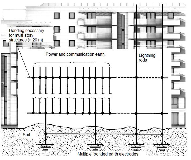
If the above mentioned conductive part is not maintained at the same potential as the earth, it is known as "floating". The issue is widely discussed in Standard 610005-2. The primary objective of an earthing system is to ensure the safety of persons and protect the installations. This particularly applies to lightning strikes and faults in the power system. By re-closing via the earth, the strong currents involved in these two phenomena can cause dangerous overvoltage. The second objective of an earthing system is to act as common reference voltage for all systems sensitive to disturbances by contributing towards their mitigation. When it comes to EMC issues, attention should be paid to the layout when an earthing system is designed, while the type and positions of the electrodes and the section of the earth conductors are relatively important, particularly at high frequencies. The recommended layout configuration is that with multiple electrodes connected to each other by equipotential bonding. In builidings over 20 meters high, these connections must be repeated every 20 meters of height (fig. 69).
Typically, each storey in an office block or industrial building has its own, generally, meshed network. These networks should be connected to each other with ≥2 bonding connections and with grounding rods. This means that there are a great number of routes for disturbances which depend on the frequency of the disturbances themselves. By and large one can affirm that the meshed earthing network covers a broad spectrum of disturbance frequencies (from 0 to tens of MHz) while vice versa, star connections between exposed conductive parts are to be avoided. In the case of industrial buildings, it is especially advisable to separate the apparatuses into zones depending on their nature and to increase the distance, as far as possible, between sources of disturbance and sensitive loads. Distance is, in fact, one of the ways to mitigate disturbance. For example, in figure 70, the computer room has its own earth while the motors, typical sources of disturbance, are bonded at a certain distance.
Figure 68: symbol of frame or chassis Figure 69: example of an earth connection in a building
