THE LATEST DEVELOPMENTS IN DUTCH SEMICONDUCTORS

THE LATEST DEVELOPMENTS IN DUTCH SEMICONDUCTORS
Semiconductors are the backbone of modern technology, facilitating advancements across myriad sectors. Indeed, from telecommunications and electronics to the automotive industry, these solutions are instrumental in the development of cloud computing, 5G infrastructure, electric vehicles (EVs), and more.
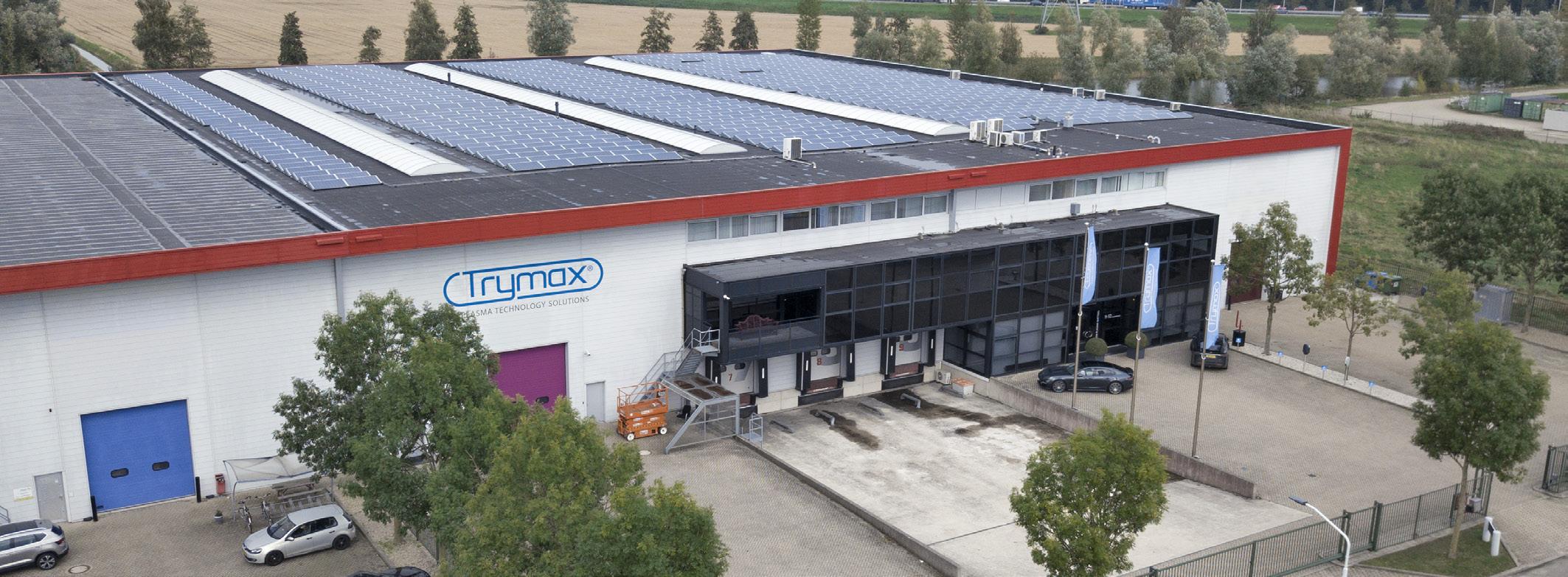
Innovative plasma-based solutions remain the core business of Trymax Semiconductor Equipment B.V. (Trymax), who stands as a
shining example of ingenuity at the crossroads of innovation and entrepreneurship in wafer manufacturing.
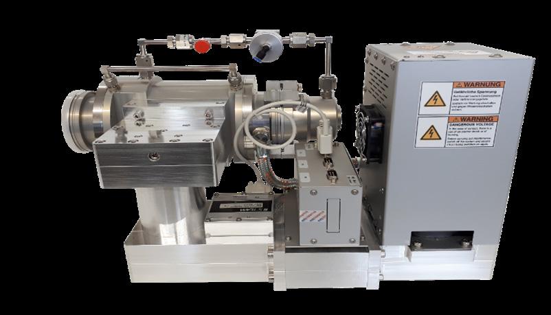
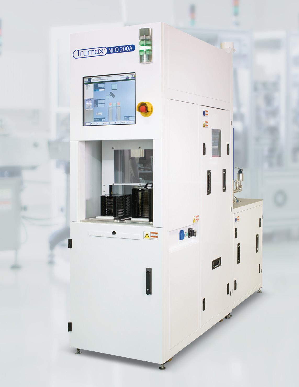
Originating as a small spinoff company founded by two former Philips engineers in the Netherlands, the Dutch company designs, manufactures, and markets its NEO series, a product line of leading-edge plasma equipment to meet the most stringent requirements and deliver advanced processing capabilities to customers.
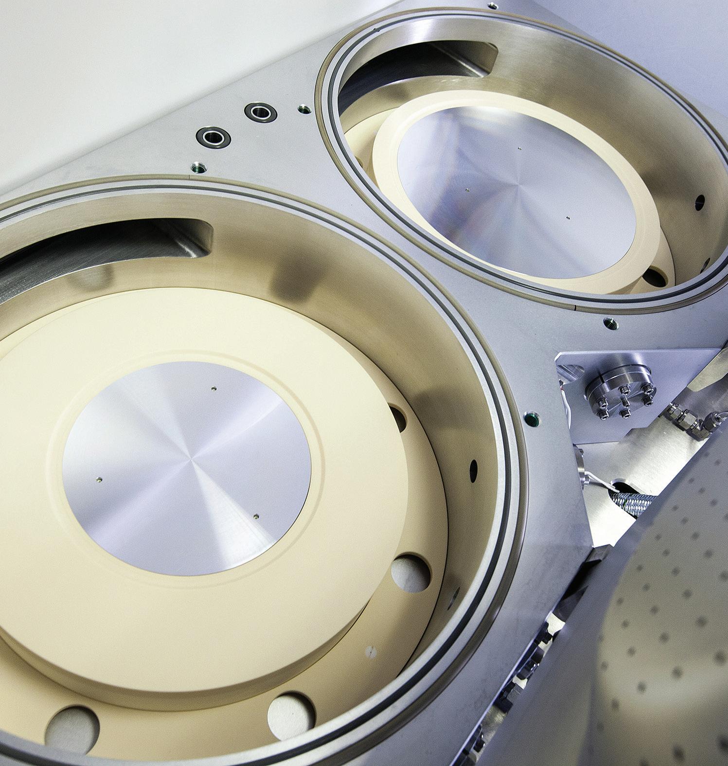
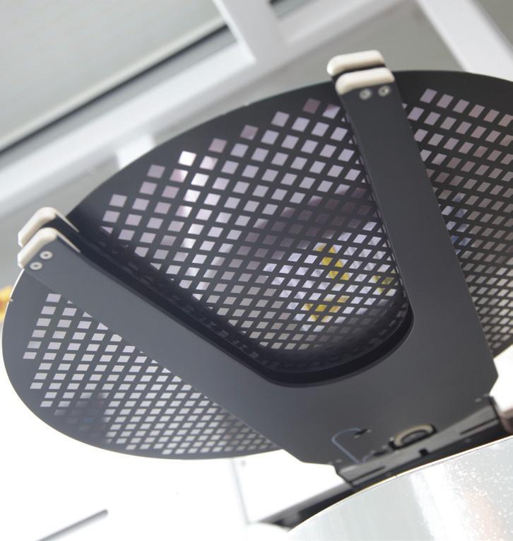
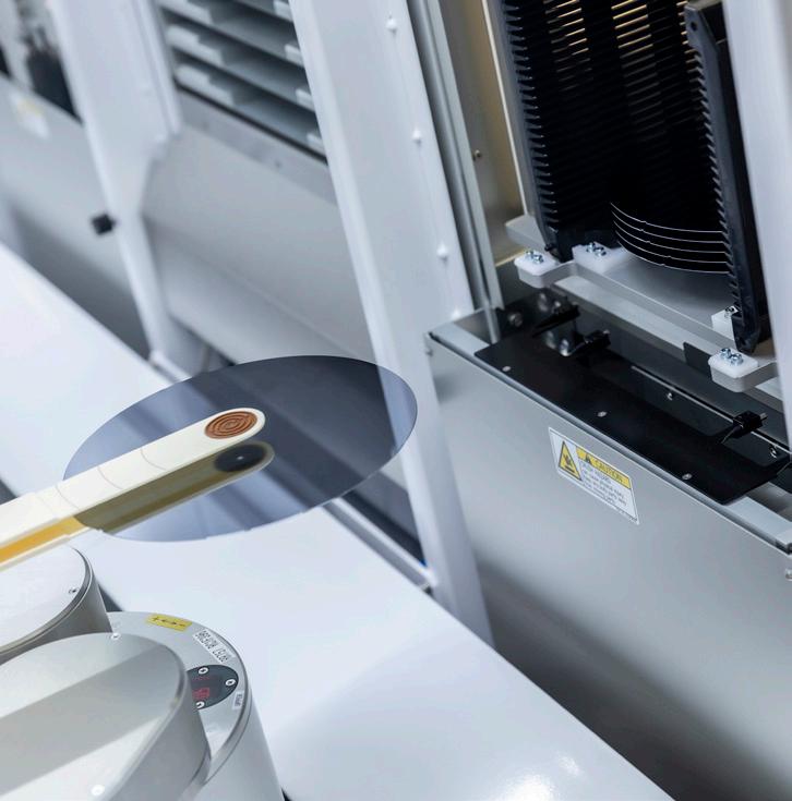
The NEO series, which can process various materials, wafer sizes, and thicknesses, addresses a number of applications during the semiconductor manufacturing process, including ashing, descumming, light etching, and surface preparation and cleaning. It also offers ultraviolet (UV) solutions for built-up device charge erasing and photoresist curing, which exhibit various benefits over baking the photoresist such as improving critical dimension (CD) control,
Peter Dijkstra, CCO, updates us on the latest developments during the past year at Trymax Semiconductor Equipment B.V., including the company’s ultraviolet solutions, notable expansion in the US, and economic mission across the pond
Writer: Jack Salter | Project Manager: Nicholas Kernan
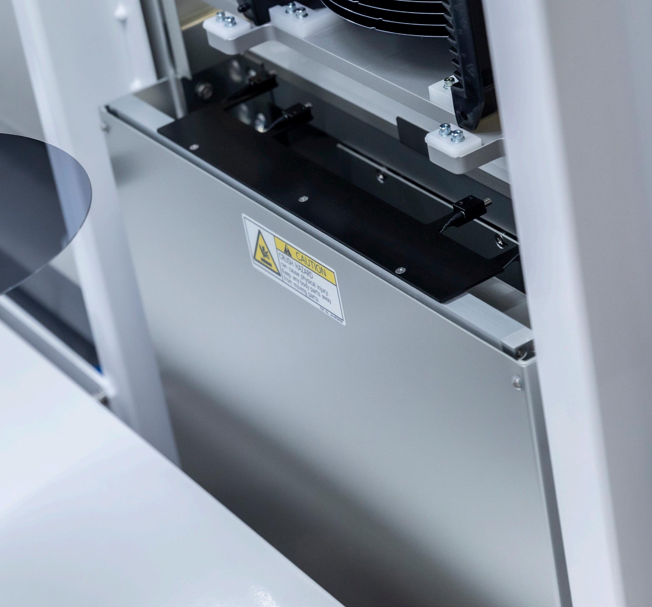
uniformity, selectivity, and overall stripping.
UV is an area in which Trymax has evolved to meet significant demand since we last spoke to CCO, Peter Dijkstra, in August 2023.
“Last year, we discussed the etching, stripping, and removal of the sensitive photoresist layer. At the same time, we also started up a new machine using UV light,” he recounts.
“If the photoresist layer has been spun on the wafer, you need a lot of water in order to equally dispatch it,
but once you’ve done that you want to remove the water to get a hard crust on top.”
To achieve this, Trymax uses UV light to quickly evaporate the water, a new tool that is replacing a lot of those currently found in the market and builds on the company’s remarkable culture and journey towards semiconductor innovation.
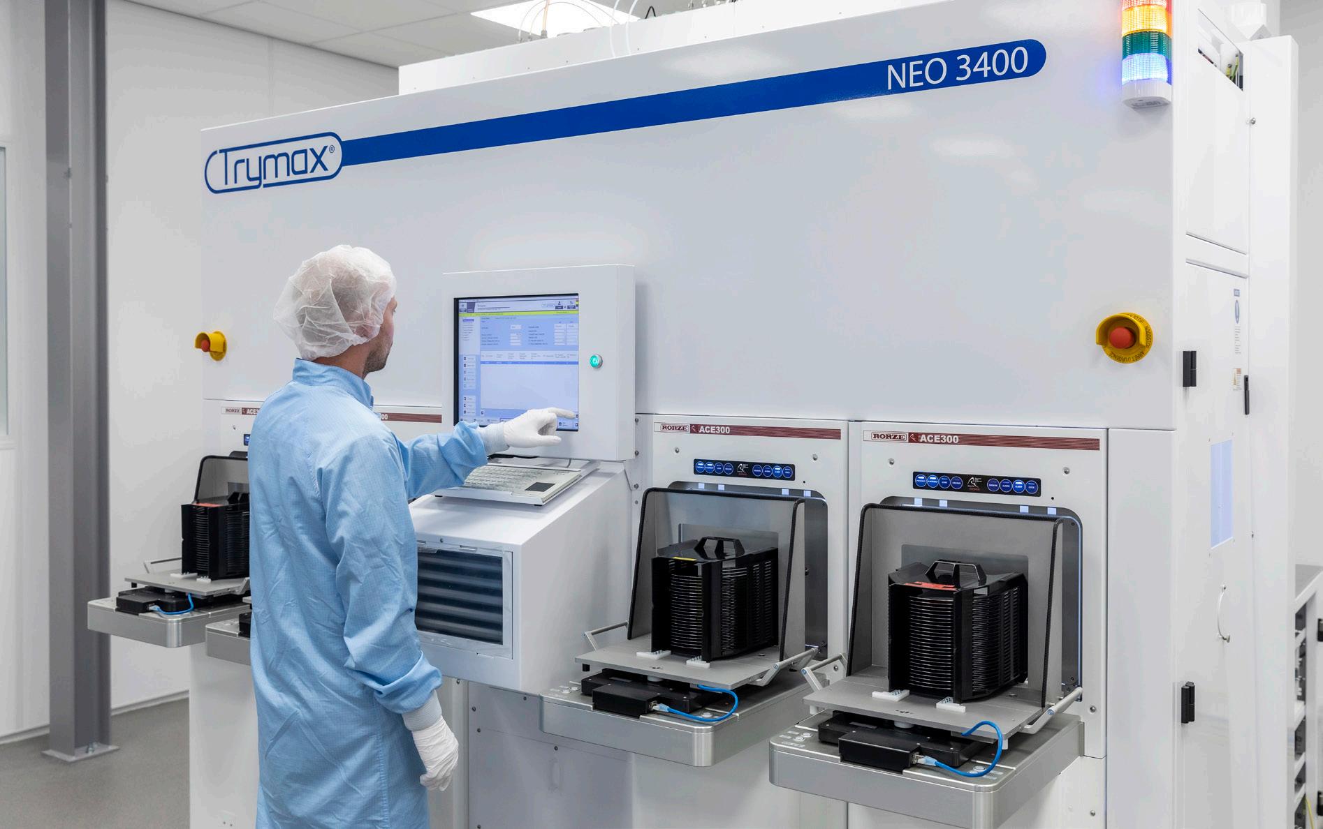
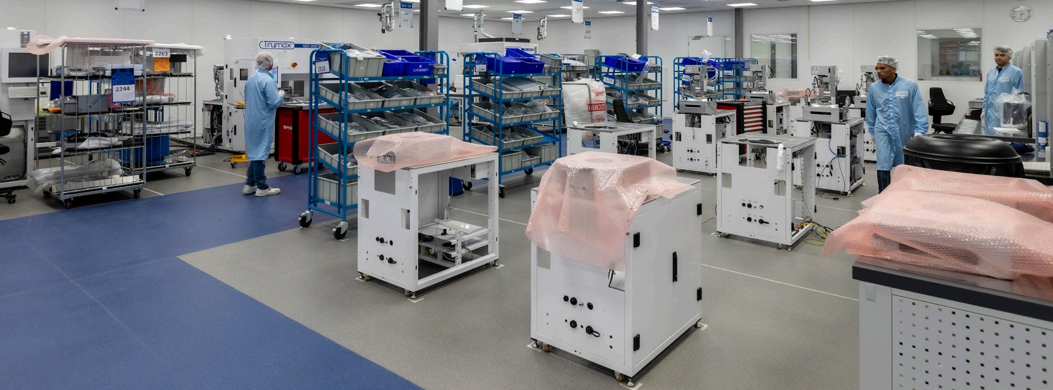
Trymax’s high-throughput NEO 2000UV system features the latest and fastest UV curing and charge erasing technology, offering
exceptional performance to meet today’s semiconductor fabrication requirements.
In January 2024, after overcoming a number of hurdles, Trymax successfully launched a start-up business in the US.
Located just outside of New York, Trymax USA Incorporated complements the company’s service office in Dallas, Texas.
Having also hired an experienced
Sales Manager and service personnel, Trymax’s operations are now fully up to speed in the country.
“We see that we are getting a lot of traction in the US at the moment,” notes Dijkstra.
The company’s expansion to the US follows the recent introduction of the Creating Helpful Incentives to Produce Semiconductors (CHIPS) and Science Act in August 2022.
The CHIPS and Science Act intends to boost American semiconductor R&D and production, ensuring US leadership in the technologies and industries of tomorrow.
Semiconductors are a US invention, however the nation today only produces around 10 percent of the world’s supply, whilst East Asia is responsible for three-quarters of global production.
“The industry in China is booming at the moment; if you look worldwide, more than half of business is coming
from China,” Dijkstra informs us.
With this in mind, the CHIPS and Science Act aims to maintain and advance the US’ scientific and technological edge by unlocking significant private sector investment in semiconductors from the likes of Trymax.
“The CHIPS and Science Act is putting quite some money on the table, so I think we are on the right track in the US at the moment,” he assures.
As well as successfully expanding in the US during the past year, Trymax was proud to be part of an economic mission on semiconductors, which took place in Arizona and California in early December.
A delegation of 45 Dutch and Flemish companies and knowledge institutes specialising in the semiconductor industry participated
in the mission along with the Dutch Prime Minister at the time, Mark Rutte.
The goal of the mission was to connect with the semiconductor and technology industry in Phoenix and the San Francisco Bay Area to exchange knowledge, seize opportunities, and accelerate innovation.
This visit coincided with rising employment numbers in the US, with more than one million American jobs supported by Dutch trade and investment, of which 78,000 are in California and 15,000 are in Arizona.
These numbers illustrate the vibrant role that the Netherlands plays in supporting a robust US economy.
“I’ve been on economic missions before, but never with the Prime Minister, and I can tell you it’s a big difference!” Dijkstra tells us.
“When the Prime Minister is incorporated, the red carpet is rolled out, all the CEOs and marketing
people are present, and you get much more traction and information than without them there.
“I think for the whole industry it was very successful, and it was nice to experience all the American policemen, the sirens, and the blue lights; it’s quite impressive to see what’s happening,” he adds.
Whereas Trymax was more equipment-oriented in the early
“THE CHIPS AND SCIENCE ACT IS PUTTING QUITE SOME MONEY ON THE TABLE, SO I THINK WE ARE ON THE RIGHT TRACK IN THE US AT THE MOMENT”
– PETER DIJKSTRA, CCO, TRYMAX SEMICONDUCTOR EQUIPMENT B.V.
days, the company has step-by-step become more process-oriented during the last 12 months.
“The customer is looking for a process solution, not an equipment solution, so little by little we are making that change,” states Dijkstra.
In this way, Trymax is now talking more about its process and application specifications with customers, rather than equipment.
One major ongoing process development at the business is what
Dijkstra refers to as ‘bowl’ or ‘wine glass’ etching.
“Silicon wires need to be cleaned but also filled with copper afterwards, which can be difficult, but if you make a wine glass opening then they’re easier to fill, so we see a lot of traction in the market for doing that,” Dijkstra explains.
The company additionally works a lot with silicon carbide wafers and is now one of the key players in this area, having supplied equipment for
Trymax has developed strong expertise in plasma equipment and processes over the last 20 years.
With more than 300 NEO systems installed worldwide, Trymax solutions are:
• High performance
• Low maintenance
• Extremely reliable
• Affordable to own
• Compact with reduced footprint
• Capable of managing multiple wafer sizes and substrate materials
• Built with state-of-the-art components, interfaces, and software
“I’VE BEEN ON ECONOMIC MISSIONS BEFORE, BUT NEVER WITH THE PRIME MINISTER, AND I CAN TELL YOU IT’S A BIG DIFFERENCE!”
– PETER DIJKSTRA, CCO, TRYMAX SEMICONDUCTOR
EQUIPMENT B.V.
multinationals in Europe, the US, and Asia.
“We are also now the number one supplier of silicon carbide equipment in China, so we are doing very well in this market segment,” he acclaims.
Acknowledging the importance of being as responsive as possible, Trymax also sets up technical review meetings (TRMs) in which the company and its customers share their respective road maps.
This makes it easier for Trymax to anticipate future requirements and have the hardware and processes ready for when customers need them.
“The whole team is very happy that we get a lot of recognition and respect in the market and that more and more people are contacting us, so we are on the right track,” Dijkstra concludes.
Tel: +31 24 350 0809 info@trymax-semiconductor.com www.trymax-semiconductor.com
Scope of Application:
• Photoresist stripping
• Isotropic etching
• Surface cleaning and conditioning
Typical etching rates are:
• Photo resist 5µm/min
• Silicon 3µm/min
• SiN and BPSG 1µm/min
• Thermal Oxide 250nm/min
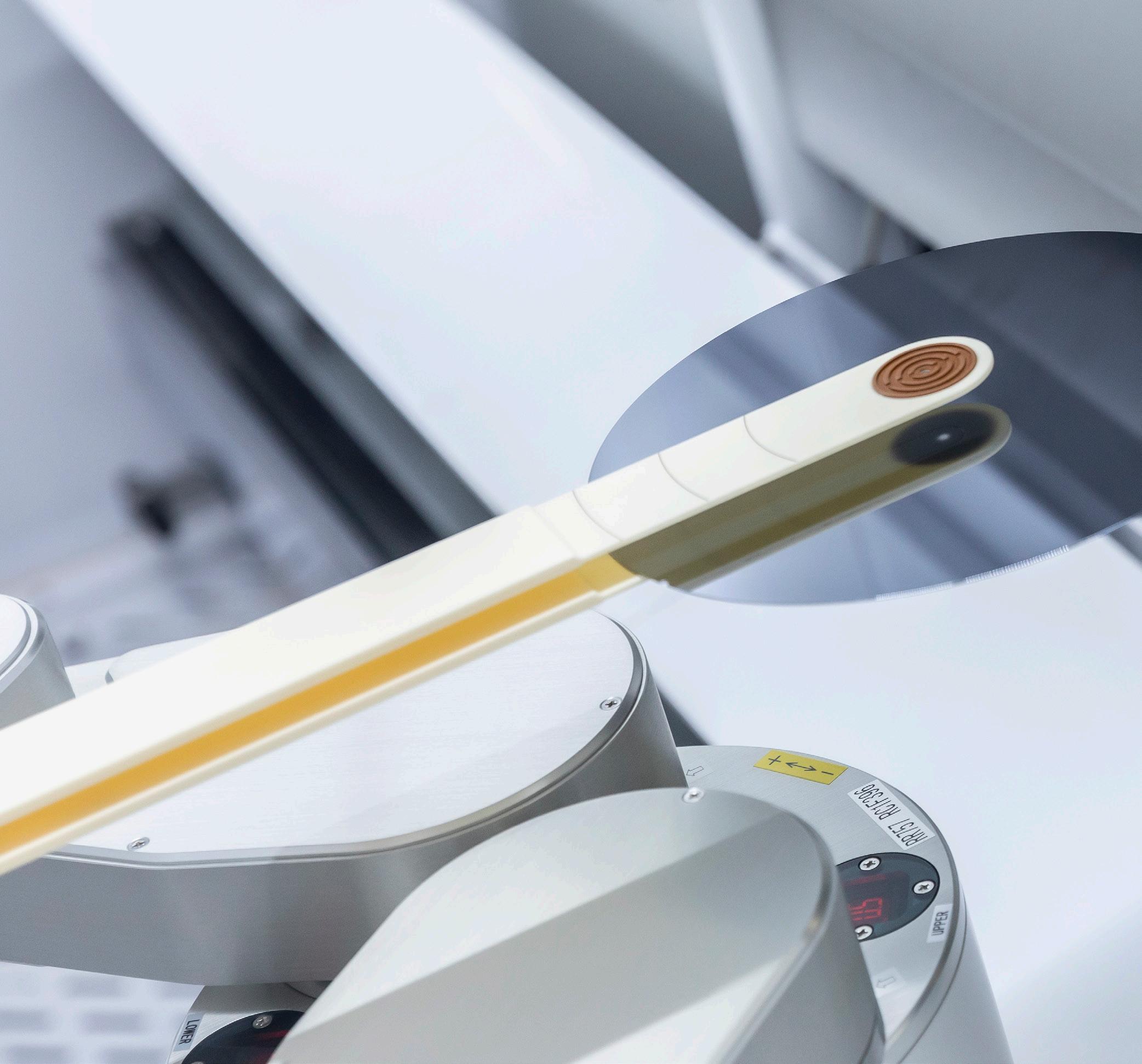
eeplasma produces microwave plasma sources for Trymax for the photoresist strip and isotropic etching processes for semiconductor production.
• The plasma sources have a maximum power of two or three kilowatts (KW) and the plasma chamber can be equipped with quartz, ceramic or sapphire tubes.
• The plasma source is characterised by its very compact design, its high level of service friendliness and its very large process window.

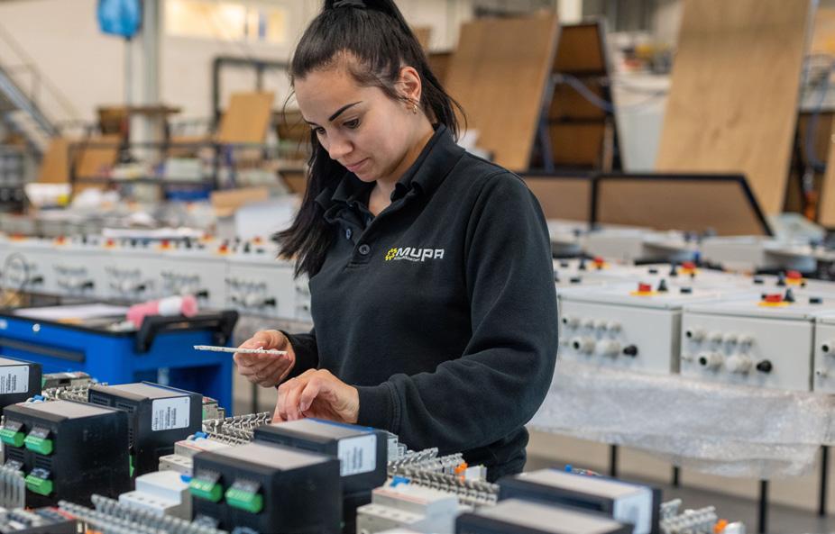
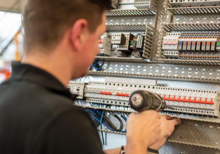
At Mupa, we passionately design and assemble high-quality control cabinets.
We deliver this on a project-based basis as well as in repetitive (series) work.
Our aim for simplicity and perfection in product and process, results in structural and long-term partnerships and added value in your process.
Mupa Schakeltechniek B.V. Meerheide 208, 5521DW, Eersel The Netherlands www.mupa.nl

It