4 minute read
AWideband 4-Level Frequency-Shift Keying Demodulator for Biomedical Implants

Abstract
A wideband 4-level frequency-shift keying (FSK) modulation scheme for biomedical implants is investigated and its digital demodulator circuits have been implemented with a 0.18m 1P6M standard CMOS technologyprocess. The application of the implementation technique is transferring data to wireless biomedical implants at a higher data-rate modulation scheme of 4-level FSK. The proposed demodulator circuits have been validated with test chip measurement results. It consumes the power of 7.2mW from a 1.8V supply.
Advertisement
Key words: 4-level FSK, biomedical implants, digital demodulators, CMOS.
1. INTRODUCTION
A high data-rate transmission is highly desired for the wireless biomedical implants, especially for those that interface with central nervous systems such as cochlears [1]-[5] which requires a large amount of data to simultaneously interface with even more amount of neurons through many channels. For wireless communication standards such as IEEE 802.11a however, the data rate can be as high as 54 Mbps with the expense of high carrier frequency even up to 5.8GHz. However, a high data-rate-to-carrier- frequency ratio with FSK modulation even up to 67% can be found in [6]-[7] at the expense of high frequency deviation (or poor spectrum efficiency) up to 2.5MHz (2-level FSK modulation scheme with 2 carrier frequencies, f1=5MHz for logic “1” and f0=10MHz for logic “0”). In this paper, the 4-level frequency-shift keying (FSK) modulation scheme is utilized, which the better performance in terms of circuit simplicity and higher data-rate can be validated with the proposed circuit experimental results.
2.THEPROPOSED4-LEVELFSKDEMODULATOR
The input RF signal is firstly down-converted to IF signal by using a down-conversion mixer and amplified to full-swing signal with an IF OTA. The demodulation is finally performed with a digital demodulator and converted back to digital data.
2.1 Mixer
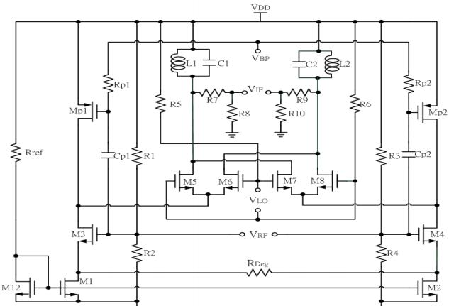
Thereceived RFsignal is down-converted to IF signal withthe double-balanced mixer as shown in Figure 2, in which a fully-differential configuration is employed [8]-[9]. It mixes the differential input RF and LO signals and develops the differential output IF signal. In Figure 2, the resonator pairs (L1, C1) and (L2, C2) act as the differential output loads in order to obtain a higher conversion gain. VBP is the bias voltage with bias resistors Rp1 and Rp2. R5 and R6 are the bias resistors providing the maximum DC level for the LO oscillator. The voltage dividers constructed with resistors R1, R2 and R3, R4 bias the differential RF port at 1V. The degenerative resistor RDeg is connected across the path between the current-mirror stages (M1 and M2) and the trans-conductance stages (M3 and M4). Thus, it does not lead to the voltage drop and still has the same linearity enhancement.
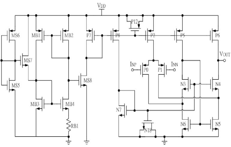
2.2 Operational Transconduction Amplifier (OTA)
In order to performdigital demodulation, the down- converted IF signal has to be full-swing with the further amplification. An OTA is employed to amplify the IF signal. Figure 3 shows the circuit of the OTA. Table 1 illustrates the performance of the OTA.
Moreover, the minimum width of the counter n is required to satisfy the relationship indicated in the follows,
Based on (1) and (2), we employ a 7-bit counter operating at 5MHz to measure the period of the received down-converted FSK full-swing signal. Note that by the employment of a 7-bit counter with 5MHz clock, it can count the longest period from the down-converted IF signal with 47.6 KHz. Also, the four different periods can represent the two-bit received data
3. EXPERIMENTALRESULTS
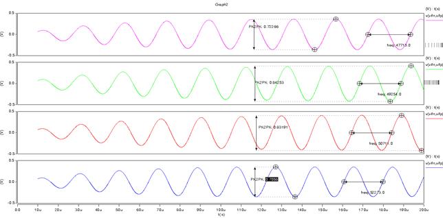
The circuit simulation of the mixer has been performed with Hspice. The amplitude level of the four RF input signals is 50mV with frequencies 9.9524 MHz, 9.9508 MHz, 9.9492 MHz, and 9.9476 MHz. They are down-converted with a local oscillator which has 200mV amplitude, 10 MHz frequency as indicated in Figure 4(a). Also note that the supply voltage VDD is 1.8V and a bias voltage VBP is 0.806V. The down-converted IFsignalscanbe obtained withthe frequencies 47.6 KHz, 49.2 KHz, 50.8 KHz, and 52.4 KHz, which the amplitude is near 386mV as shown in Figure 4(b).
2.3 Digital Demodulator
In the proposed digital approach for FSK demodulation, the periods of the four down-converted intermediate- frequency (IF) carriers are measured by the employment of a binary countertriggered withhigherfrequencyclock, which is similar to the previous publication [6] whereas in our approach we measure the whole period which can have more duration to discriminatebetweenthefour IF carrier frequencies. Intheory, the relationship between the clock frequency and the four IF carrier frequencies can be described as follows,
Figure digital
Four carrier frequencies of the received down-converted FSK signals, 52.4 KHz, 50.8 KHz, 49.2 KHz and 47.6 KHz represent received demodulated data 2’b11, 2’b10, 2’b01, and 2’b00, respectively and the counter will detect and measure the periods of the FSK carrier signals.
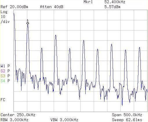

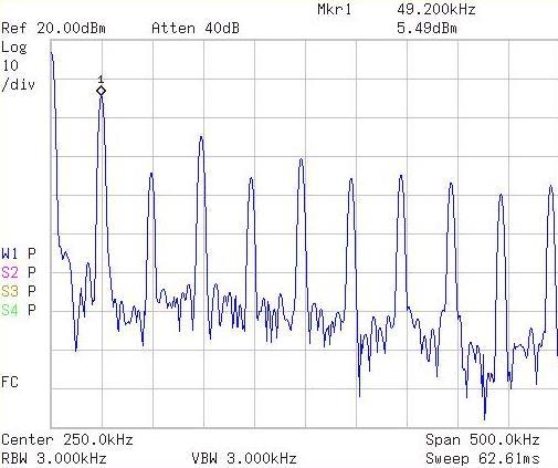

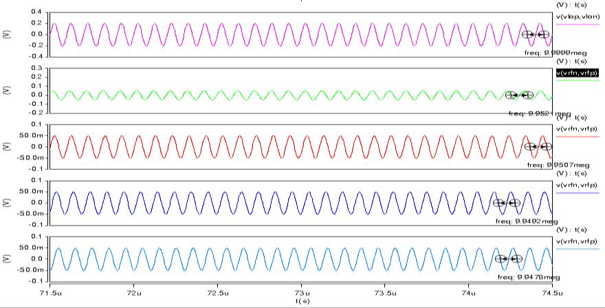
The measurement results of the down-conversion mixer are shown in Figure 7. Obviously, the down-converted IF signals are much higher than their harmonics for each case. (a)

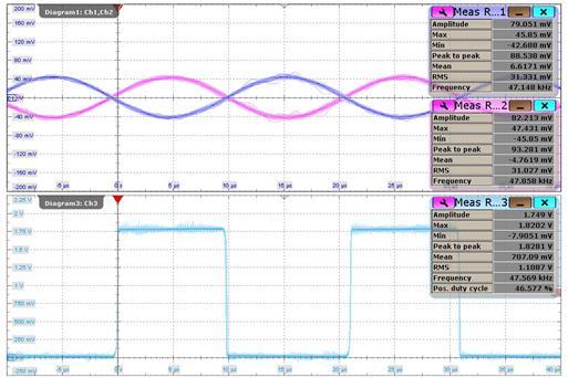
The measurement results of the OTA output clock signals are shown in Figure 8. The upper channel shows the differential input of the OTA and the lower channel indicates the single-ended output full-swing signal of the OTA for the next digital demodulator stage.


(a)
(d)
49.2KHz (c) 50.8KHz (d) 52.4KHz.
The implementation of the digital FSK demodulator has been performed with Verilog HDL and synthesized with Synopsys DesignCompiler. Inorder to provide bit error tolerance due to the received IF signal jitter, the circuit design can tolerate two-bit error. In other words, we can obtain count ‘105’ for a 47.6 KHz IF signal with the input 5MHz-clock signal for the counter. However, due to the jitter effect on the received 47.6 KHz IF signal, the count can be ranged between ‘104’ and ‘106’, which is equivalently near 0.53KHz frequency deviation. Under this circumstance, the same code will be assigned. Moreover, larger jitter tolerance can also be achieved bythe employment of higher-frequency clock for the counter whereas it can consume more power. Table 2 reveals the specifications of the 4-level FSK demodulator circuits and Table 3 summaries the performance of the realized chip.
(b) (c)
Other Frequencies = 0000000
