3 minute read
SHORTcircuits


INNOVATIVE NEW METHOD CONTROLS OPTICAL CIRCUITS ON PICs
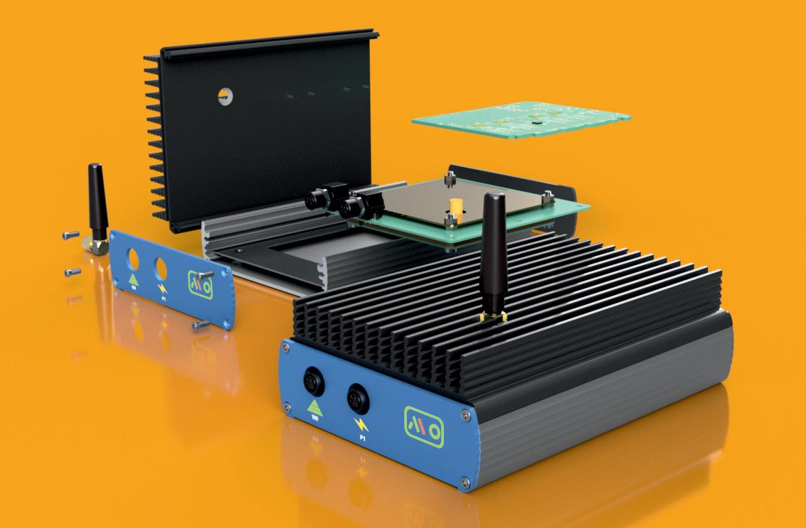
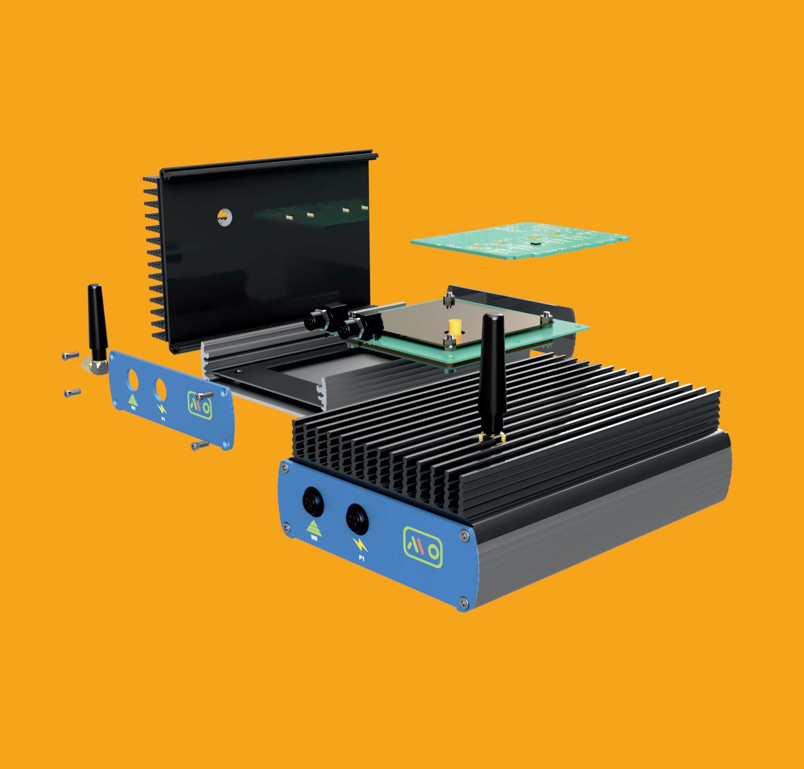
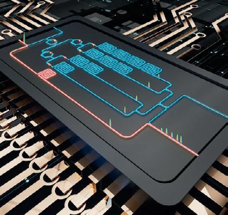
Researchers from Monash University, RMIT and the University of Adelaide have developed a method to control optical circuits on fingernail-sized photonic integrated circuits. Photonics, or the use of light particles to store and transmit information, is a burgeoning field, supporting the need to create faster, better, more efficient and more sustainable technology. Programmable photonic integrated circuits (PICs) offer diverse signal processing functions within a single chip, and present solutions for applications ranging from optical communications to artificial intelligence. Photonics is also changing the processing capability of large-scale equipment onto a chip the size of a human fingernail.
Earlier this year, researchers at Monash University, RMIT and the University of Adelaide developed an advanced photonic circuit that could transform the speed and scale of photonics technology. However, as the scale and complexity of PICs grows, the characterisation and calibration of them becomes increasingly challenging. Monash University research fellow Professor Mike Xu said the team added a common reference path to the chip, which enables stable and accurate measurements of the lengths (phases, time delays) and losses of the ‘workhorse’ paths. “By inventing a new method, the fractional delay method, we have been able to separate out the wanted information from the unwanted, making for more precise applications,” Xu said.
Previously chips have been measured/calibrated by connecting to complex and expensive external equipment (called a vector network analyser); however, the connections to it introduce phase errors, caused by vibrations and temperature changes. By putting the reference on the actual chip, these phase errors can be avoided. Professor Arthur Lowery from Monash University said that previously, researchers used the ‘Kramers–Kronig’ method to remove unwanted errors from desired measurements, but the fractional method requires less optical power for calibration for a given accuracy. “This means that we can get reliable measurements of the chip’s status, so are able to accurately program it for a desired application, such as pattern recognition in an optical computer, or squeezing extra capacity from an optical communications network,” Lowery said.
In the next phase of development, this research team will explore how photonic chips can use many wavelengths to achieve ultrafast information processing and machine intelligence.
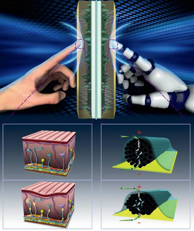
Bionic Finger Renders 3d Images Of Electronic Devices
Researchers have presented a bionic finger that can create 3D maps of the internal shapes and textures of complex objects by touching their exterior surface. Senior author Jianyi Luo, a professor at Wuyi University, said the researchers were inspired by human fingers, which have the sensitive tactile perception. “For example, when we touch our own bodies with our fingers, we can sense not only the texture of our skin, but also the outline of the bone beneath it,” Luo said.
The bionic finger ‘scans’ an object by moving across it and applying pressure, akin to a constant stream of pokes or prods. With each poke, the carbon fibres compress, and the degree to which they compress provides information about the relative stiffness or softness of the object. Depending on the object’s material, it might also compress when poked by the bionic finger: rigid objects hold their shape, while soft objects will deform when enough pressure is applied. This information, along with the location at which it is recorded, is relayed to a personal computer and displayed onscreen as a 3D map.
The researchers tested the bionic finger’s ability to map out the internal and external features of complex objects made of multiple types of material, such as a rigid ‘letter A’ buried under a layer of soft silicon, as well as more abstractly shaped objects. When the finger was used to scan a small compound object made of three different materials — a rigid internal material, a soft internal material and a soft outer coating — it was able to discriminate between the soft outer coating and the internal hard ridges, and could also tell the difference between the soft outer coating and the soft material that filled the internal grooves.
The researchers also explored the bionic finger’s ability to diagnose issues in electronic devices without opening them up. By scanning the surface of a defective electronic device with the bionic finger, the researchers could create a map of its internal electrical components and pinpoint the location at which the circuit was disconnected, as well as a mis-drilled hole, without breaking through the encapsulating layer.
“Next, we want to develop the bionic finger’s capacity for omnidirectional detection with different surface materials,” Luo said.