
15 minute read
Considerations when specifying enclosures for Industry 4.0 applications


Pat Cookson
Industry 4.0 — the deployment of distributed automation and data exchange in manufacturing technologies — is based around the Internet of Things (IoT) and cloud computing to create the ‘smart factory’, where physical machines are monitored and controlled in pseudo real time and autonomous decentralised decision-making manages the process.
The move to complex distributed computing brings with it some high-level technical issues: IT security, greatly aggravated by the inherent need to open up previously closed production systems; the need for high levels of IT system reliability; the repeatable low system latency requirements and stability needed for critical machine-to-machine communication; and the need to maintain the integrity of production processes. The distributed mini-systems will often have embedded IP capability, Wi-Fi and Bluetooth connectivity, processing and communicating information from their attached sensors and controls throughout the IoT rather than raw signals going back to a central control room. In addition to these macro level concerns, at the micro level the widespread distribution of electronic modules and subsystems in the factory environment requires considerable thought to be given to the selection of the housing for the electronics. Given that the selected enclosure must provide a secure and physically robust environment for the electronics, there are several criteria to consider when choosing the optimum product design.
A standard or applicationspecific design?
Selecting a standard enclosure from one of the many suppliers has some obvious benefits: there are no upfront non-recurrent design, engineering and tooling charges; products are on the shelf ready for immediate delivery, so time to market is low; the unit costs are attractive; and the design will have been field proven in many different applications. Compared with an application-specific custom enclosure, designed specifically for the project, standard products are immediately available and, certainly in volumes up to the low thousands, are extremely cost-effective.
However, any standard enclosure will need modifying to meet the requirements of
a specific application, requiring machining with suitable apertures to accept switches, displays, I/O connectors and other components. They will also need to be printed with legends and logos. The best option is for the original manufacturer to provide a modified enclosure configured to the specific requirements of the equipment. It is certainly of great benefit to involve the standard enclosure manufacturer as early as possible in the development cycle. There is no need to over-order to allow for setup and wastage quantities if the standard enclosure is purchased and the modifications outsourced to one or more suppliers.

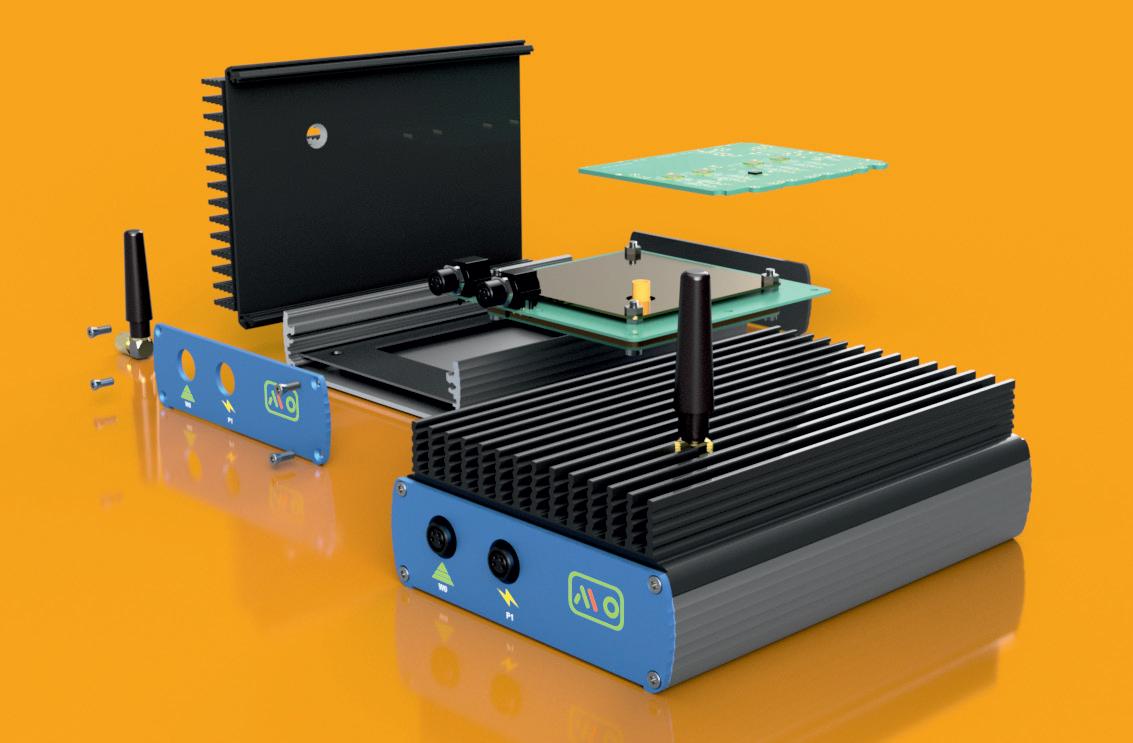
Physical protection
Small enclosures are usually made from die-cast or extruded aluminium or are moulded from flame-retardant or standard ABS or polycarbonate. As all materials have specific properties in terms of impact resistance, resistance to chemicals, resistance to abrasion and so on, the choice of material will to a certain extent be controlled by the location and expected environment.
Environmental protection
By definition, Industry 4.0 requires electronic modules and systems to be installed on the factory floor, close to the equipment that is being monitored and controlled. The question of the level of protection against the ingress of dust and water therefore becomes significant in the specification criteria, defined in EN 60529 as IPxx, where the first digit
defines the protection against solid objects and the second the protection against water ingress. An enclosure for general-purpose use would typically be rated IP54, whereas one for use in hostile environments would need to perform to a minimum level of IP65, but nowadays IP67 is becoming the de facto minimum requirement.
In general, enclosure manufacturers use two main techniques to achieve the designed protection level. Satisfactory IP54 sealing is readily achieved by using a tongue and groove construction to the joint between the body of the enclosure and a removable panel or lid. No gaskets are used; the seal is achieved through the combination of a recess in the base section that mates to the corresponding mirror profile in the lid when the lid is screwed down. To achieve higher levels of sealing in metal, plastic and extruded small enclosures will require a gasket between the two mating halves. Normally a separate, preformed moulded gasket is sandwiched between the two mating surfaces. A metal enclosure can be painted if required without having to mask the gasket area; the gasket can be easily replaced if it is damaged.

EMC performance
In many applications EMC capability is of no interest, but in the potentially electrically noisy factory floor environment, it can be a consideration. Moulded enclosures have one specific weakness: by virtue of the intrinsic properties of the material itself, plastic, unlike metal, offers no inherent attenuation to the passage of electric or magnetic fields. If EM radiation emitted by the housed electronics or their susceptibility to external fields is a potential problem, the lack of screening could be an issue.
Internal coatings in a variety of materials can be applied to the inner surfaces of a plastic enclosure to give different degrees of attenuation dependent on the project requirements. By offering different materials in a range of thicknesses, the most costeffective and technically competent solution can be provided. Metal enclosures, providing they are manufactured in such a way that electrical continuity is present between the top, base and removable panels and that any painted or anodised finish is purely for external decorative purposes, will provide a level of EMC likely to be more than sufficient for the majority of applications.

Heat dissipation
With small low-power systems, heat dissipation is not usually an issue, but if systems are generating sufficient waste heat it can become a problem. As with EMC, metal and plastic enclosures have significantly different properties. Metal enclosures have greater ability to provide conduction and convection cooling because of their greater conductivity; indeed, some extruded enclosures are designed with increased surface area to improve cooling performance. All types of enclosure can be modified with arrays of holes to improve convection cooling if required.
Modifications
In order to make a standard enclosure suitable for a specific use, it will need to be modified. The purchaser has three main options. 1. Purchase standard products, either directly from the manufacturer or through distribution, and then modify them as required in-house. However, many electronic OEMs may not have the plant, equipment, expertise or interest in undertaking machining and painting procedures in their own premises. If there is in-house capability, to modify the housing as a part of the overall assembly process could be the best way to proceed. However, more standard units than are actually required will have to be purchased to allow for set-up procedures and wastage. 2. Buy standard products and outsource the modification processes to external contractors. This will incur additional costs, time penalties and logistics complications associated with managing the process of subcontracting, often to multiple suppliers, potentially further increasing the costs as each process will require extra units to allow for first-offs and set-up wastage. 3. By far the best option is for the original manufacturer to provide a modified enclosure configured to the specific requirements of the project. With this option, there is no need to over-order to allow for set-up and wastage quantities. Hammond Electronics has a long-established network of international and national broadline catalogue and specialist distributors throughout Europe. The close working relationship between Hammond and the distribution partners means that factory modified enclosures can be sourced from the distributor or from Hammond direct.
Enclosure manufacturers will typically be able to provide milling, drilling, punching, engraving, screen printing, painting and EMC coatings for their range of standard products. Manufacturers of moulded enclosures can normally also offer enclosures moulded in custom colours to meet any applicable identifying requirements or corporate branding needs.

NanoEdge AI Studio
Development tool to quickly add machine learning to deep edge devices

• Easy-to-use desktop tool to create optimized Machine Learning libraries to address anomaly detection, classification or extrapolation problems • Turnkey solution that requires no specific AI or data science skills • New algorithms to better predict equipment anomalies and future behaviour • High-speed data acquisition and management capabilities • Can generate small footprint libraries for all the STM32 portfolio, including the smallest Arm® Cortex®-M0-based MCUs • Compatible with all types of sensors • Native support for all STM32 development boards
www.st.com/en/development-tools/nanoedgeaistudio
SHORTcircuits
© Stock.Adobe.com/au/adimas

Researchers from the University of Surrey’s Advanced Technology Institute (ATI) and the University of São Paulo have developed a new analysis technique that should help scientists improve renewable energy storage by making better supercapacitors. Published in the journal Electrochimica Acta, the new approach enables researchers to investigate the complex interconnected behaviour of supercapacitor electrodes made from layers of different materials.
Improvements in energy storage are vital if countries are to deliver carbon reduction targets. The inherent unpredictability of energy from solar and wind means effective storage is required to ensure consistency in supply, and supercapacitors are seen as an important part of the solution. However, more supercapacitor development is needed to enable them to effectively store enough electricity.
In light of this, the research team used a cheap polymer material called polyaniline (PANI), which stores energy through a mechanism known as pseudocapacitance. PANI is conductive and can be used as the electrode in a supercapacitor device, storing charge by trapping ions.
To maximise energy storage, the researchers developed a novel method of depositing a thin layer of PANI onto a forest of conductive carbon nanotubes. This composite material makes an excellent supercapacitive electrode, but the fact that it is made up of different materials makes it difficult to separate and fully understand the complex processes which occur during charging and discharging.
To tackle this problem, the researchers adopted a technique known as the distribution of relaxation times. This analysis method allows scientists to examine complex electrode processes to separate and identify them, making it possible to optimise fabrication methods to maximise useful reactions and reduce reactions that damage the electrode. The technique can also be applied to researchers using different materials in supercapacitor and pseudocapacitor development.
“The future of global energy use will depend on consumers and industry generating, storing and using energy more efficiently, and supercapacitors will be one of the leading technologies for intermittent storage, energy harvesting and high-power delivery,” said Ash Stott, lead scientist on the project from the University of Surrey. “Our work will help make that happen more effectively.”
“Our work shows researchers how to accelerate the development of high-performance materials for use as energy storage elements, a key component of solar or wind energy systems,” added ATI Director Professor Ravi Silva, principal author on the study.

USING NUCLEAR RADIATION TO TRANSMIT DIGITAL DATA WIRELESSLY
Radio waves and mobile phone signals typically rely on electromagnetic radiation for communication. Now engineers from Lancaster University in the UK, working with the Jožef Stefan Institute in Slovenia, have transferred digitally encoded information using nuclear radiation instead.
The researchers measured the spontaneous emission of fast neutrons from californium-252, a radioactive isotope produced in nuclear reactors. Modulated emissions were measured using a detector and recorded on a laptop.
Several examples of information, ie, a word, the alphabet and a random number selected blindly, were encoded serially into the modulation of the neutron field and the output decoded on a laptop, which recovered the encoded information on-screen. A double-blind test was performed in which a number derived from a random number generator was encoded without prior knowledge of those uploading it, and then transmitted and decoded. All transmission tests attempted proved to be 100% successful.
“We demonstrate the potential of fast neutron radiation as a medium for wireless communications for applications where conventional electromagnetic transmission is either not feasible or is inherently limited,” said Professor Malcolm Joyce of Lancaster University. He explained that fast neutrons have an advantage over conventional electromagnetic waves, which are significantly weakened by transmission through materials including metals.
“In some safety-critical scenarios, such as concerning the integrity of reactor containments, and metal vaults and bulkheads in maritime structures, it can be important to minimise the number of penetrations made through such metal structures for communications cabling,” Prof Joyce said.
Fast neutrons could also be incorporated into a mixed-signal, electronic system to achieve signal-mixing between electrons and neutrons. This could contribute to the requirement to ensure the integrity of information transfer.
© Stock.Adobe.com/au/wlad074


SHORTcircuits
© Stock.Adobe.com/au/black_kira

Researchers at Germany’s Karlsruhe Institute of Technology (KIT) have developed an innovative concept for simultaneous coating and drying of two-layered electrodes. Drying times can be reduced to less than 20 seconds, which corresponds to half down to one-third of the usual production time, without capacity losses. Lithium-ion batteries can thus be produced more rapidly and at lower cost.
In lithium-ion batteries, electrode layers are of decisive importance, as these active materials store the energy. However, coating and subsequent drying of electrodes cause most of the battery production costs. A big cost reduction potential lies in process engineering. Researchers from KIT’s Thin Film Technology (TFT) group, headed by Professor Wilhelm Schabel and Dr Philip Scharfer, have already succeeded in considerably increasing coating speed and developed an innovative drying process.
“Our work shows that in principle, we manage all process steps needed to produce batteries more rapidly and, hence, at lower cost in future without affecting quality,” Prof Schabel said.
At usual electrode drying times of up to one minute and production speeds of 100 m/min and more, long drying lines are needed. In case of electrodes with a high coating weight, this is hardly feasible and very expensive. The new concept is based on the idea of using different active materials for the layers and applying them simultaneously. One layer is responsible for adhesion and another for specific capacity. This layer structure enables manufacture at a very high drying rate, so drying times are shortened to one-third.
In spite of the reduced drying time, no capacity losses occur and the range of the battery remains the same. The scientists also applied different active materials over the thickness of the anode, as a result of which different properties were distributed specifically in the electrode layers. In this way, electrodes can be customised and have better mechanical and electrochemical properties.
“Our research demonstrates that it may be possible in principle to increase battery production speed by 200–300%,” Prof Schabel said.
At the moment, the group is working on ways to transfer the simultaneous concept to the industrial scale. For this purpose, it tests purely convective drying with high-performance nozzles and laser drying modules. The results are also being transferred to other materials and used to optimise electrodes of sodiumion batteries within Germany’s Post Lithium Storage Cluster of Excellence (POLiS).

LIGHT SENSORS OPTIMISED FOR THE IoT ERA
Scientists from Incheon National University have developed a compact and robust optical sensor that can convert light to digital signals, making it ideal for deployment in the so-called ‘trillion-sensor era’ of the Internet of Things (IoT). Their research has been published in the journal Small.
An important part of the IoT economy is the presence of light/ photo sensors, which are tiny semiconductor-based electronic components that detect light and convert it to electrical signals. Light sensors can be found everywhere around us, from household electronic gadgets and healthcare equipment to optical communication systems and automobiles.
Most light sensors used in cost-effective consumer products are energy efficient but are susceptible to noise (unwanted light information) in the external environment, which adversely affects their performance. To tackle this issue, products have been designed using light-to-frequency conversion circuits (LFCs), which show better signal-to-noise ratio. However, most LFCs are made of silicon-based photodetectors that can limit the range of light detection. Also, use of LFCs leads to chip area wastage, which becomes a problem when designing multifunctional electronic circuits for compact devices.
Led by Professor Sung Hun Jin, Incheon researchers demonstrated a highly efficient system of photodetectors that can overcome the limitations of conventional LFCs. They developed complementary photosensitive inverters with p-type single-walled carbon nanotubes (SWNT) and n-type amorphous indium–gallium–zinc–oxide (a-IGZO/ SWNT) thin film transistors.
The new design architecture allowed the team to design an LFC with high chip area efficiency and a compact form factor, making it suitable for use in flexible electronic devices. Experiments conducted using the photosensor system indicated excellent optical properties, including high tunability and responsiveness over a broad range of light. The LFC also showed possibility of large-area scalability and easy integration into state-of-the-art silicon wafer-based chips.
The LFC system could be used to build optical sensor systems that have high-level signal integrity, as well as excellent signal processing and transmitting abilities. These promising properties make it a strong contender for application in future IoT sensor scenarios, such as medical SpO2 detection, auto-lighting in agriculture, or advanced displays for virtual and augmented reality.
© Stock.Adobe.com/au/asb64


