4 minute read
QUALITY CONTROL


Quality assurance can tackle the intricacies of flexible circuits
Here’s how advances in testi ng can improve feature inspecti on.
Timothy Weber | Buehler | F lexible circuits may seem to be a recent development, but they date back to German inventor Albert Hanson in 1898. He described the production of fl at conductors on a paraffi n-coated sheet to improve telephone exchange boards.
What fl exibility the waxed paper provided, it lacked in durability. Flexible circuit creators today sandwich them between a polymer cover layer and base fi lm of either polyimide or polyester. Designers favor polyimide where soldering of the assembly is required, and it is the material of choice for nearly all chip-scale packages and fl ex ball grid arrays.
The wider application of fl exible circuits took the recent development of new materials and manufacturing techniques, enabling the design to recently become one of the fastestgrowing segments of the global printed circuit industry. New applications, usually involving smaller, more mobile devices, have pushed this expanded use along, particularly in the medical fi eld.
Circuitry in medical devices — a tight squeeze
Medical device product specifi cations can limit space available for circuitry. A multilayer fl exible circuit board can handle all the control functions of a complex medical device and provide greater functionality.
Evolving design can pose manufacturing and testing challenges. PCB manufacturers are fi nding that thinner material leads to smaller vias, a reduced aspect ratio of vias, smaller lines and spaces, less copper plating and better fi ll grades, but it can also increase handling complexity.
Flexible circuits’ quality assurance needs differ from rigid PCBs’. In response, testing systems manufacturers are developing new products and techniques to inspect features such as vias and through-holes. These approaches meet the unique needs of increasingly smaller and lighter fl exible circuits demanded by the medical market.
Metallography plays an integral role in analyzing and understanding the effects of these improvements on the PCB internal structure. Quality control benefi ts from evaluating the product at various stages of a new production process. Crosssectioning samples can reveal vital details, including cracks, voids, conducting layers and interconnections.


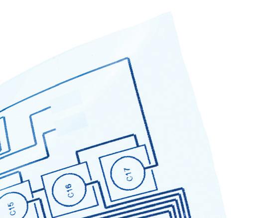
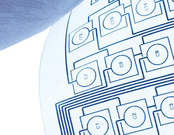
Flexible medical circuit
Images courtesy of Buehler


Isolating problems and finding improvements
In other cases, a more targeted approach involves crosssectioning the center-line of through-holes or progressively thinning the specimen and examining each layer. The more information gathered during an analysis, the higher the probability of improvement.
Labs cut these boards using a precision saw to minimize the potential for damage to the board. Cutting and handling these boards inappropriately can cause defects such as delamination — sometimes incorrectly attributed to the manufacturing process.
Testing equipment manufacturers offer precision saws with table attachments. These saws enable the testing lab to quickly cut flex and hybrid boards without damaging the area of interest while providing a higher degree of safety for operators than band saws or hand tools.
Flex circuits and the hybrid rigid-flex circuits in medical devices present a more significant challenge in targeting regions of interest. The same properties that make these board materials (often PEEK or polyamide) useful also introduce the potential for inaccuracies.
Dealing with small feature size
Note that these features are, in many cases, quite small, ~100 microns or even less. It’s necessary to avoid pin placement variability (when pinning boards for processing) or positioning of board coupons in the accessory when mounting.
These boards are often very light compared with rigid PCBs. Care is needed to prevent coupons from “floating” in media during mounting, leading to inaccuracy in targeting.
Reduced feature size has been the trend, along with the miniaturization of medical devices. Smaller feature size enables flexible boards to have multiple rows of features, often at varying dimensions within the same board. These boards have targeted features of varying sizes and features placed at different distances from a reference within the board.
Testing equipment manufacturers have developed accessory kits for semi-automatic grinder-polisher equipment that can target these smaller features. These latest kits can target such features in relatively high production volume, with up to 18 PCBs processed in less than 30 minutes. These newer accessory kits also have a significantly reduced cost.
They can also handle tighter tolerances that have been specified on small features, use polycrystalline diamond stops that resist wearing when compared to mono-crystalline or carbide stops, and reduce the span of the reference pins used in the kit, ensuring these features are presented in a plane perpendicular to the view under the microscope. Kit manufacturers can provide technical expertise specifically for users working with small (<= 4 mil) feature sizes and aspects of preparation to pay particular attention, which enhances the capability of success in targeting.
In addition to these developments in PCB production, preparation, and inspection, there has been an increased demand for reliability. Accordingly, addendums to IPC standards have been published not only for medical devices but other industry segments such as aerospace and automotive.
Proper preparation provides the capability to verify reliability standards. Testing equipment manufacturers continue to work with many PCB manufacturers to ensure compliance with IPC specifications.

Bi-directional flex circuit, a multilayer flex circuit cross-section as polished at 100x