
46 minute read
Madhukar Tripathi
(2) Requires efficient I&M under severe security administration
Data center sites are subject to severe security administration requiring I&M work to be performed during restricted time periods. Performing tests of the various communications standards for Metro DCI requires trained and experienced operators with good knowledge about communications and network I&M.
Advertisement
(3) Requires optical fiber maintenance
Metro DCI network configurations use fast high-capacity optical fibers. In addition to conventional optical loss measurements, fast DCI optical fibers must be evaluated for optical reflections. The IEEE802.3 100GBASE-LR4 and 10GBASE-LR standards specify an optical fiber connector reflection loss of not more than 26 dB. Generally, SPC and UPC fiber connectors have a reflection loss of about 40 dB and 50 dB, respectively, but if the connector end face is contaminated with oil, dust, etc., the optical loss increases due to the increased optical reflections caused by the contamination, resulting in degraded communications quality. Appropriate maintenance at optical fiber I&M is key to preventing communications problems.
Metro DC Optical Fiber
WDM Circuit
Optical Fiber
Metro DCI Connections
Optical Fiber
Metro DC
Optical Fiber Cladding

Oil and Dust Contaminauts
Contaminated Optical Fiber End Face
Top of Rack (TOR) architecture is where the cabling between switch and server stays within a rack. This has the benefit of reducing the overall amount of cabling with the downside of reduced efficiency in the usage of Ethernet switch ports which are limited to within a rack.
Following measurements at Data Center (DC) Interconnect I&M are conducted. • BER: BER is one of the basic measurements and includes include Frame Loss and Sequence Error tests. • Latency: Network latency is the time it takes for data or a request to go from the source to the destination. Latency in networks is measured in milliseconds. The closer your latency is to zero, the better. • Throughput: Throughput measures how many packets arrive at their destinations successfully & is measured in bits per second. Packet loss, latency, and jitter are all related to slow throughput speed.
BER Test: BER test consist of many tests such as Generation and detection of test patterns, Count of errors in received test pattern, Pattern generation: Unframed (Layer 1), Framed Ethernet (MAC) header (Layer 2), Framed Ethernet (MAC) header with IP header (Layer 3) or Framed Ethernet (MAC) header, Framed with IP header and TCP/UDP header (Layer 4), User-defined header pattern (14 byte to 256 byte), Detection of sequence errors, loss of sequence synchronization, Frame loss count and frame loss seconds.
Throughput measurement results are calculated for: • Utilization layer, Physical layer, Physical layer excluding preamble, Link layer, Network layer and Data layer • Min./Max./Avg. values Performance (M.2100 type) parameters: ES, SES, ALS, UAT, AVT, EFS Test patterns: PRBS 9, PRBS 11, PRBS 15, PRBS 20, PRBS 23, PRBS 29, PRBS 31, HF test pattern, CRPAT, JTPAT, SPAT, 55 Hex, Fox, 32-bit user programmable User-defined resolution: 1, 2, 5, 10, 15, 30 s, 1, 5, 10, 15, 30 min, 1, 2, 4, 6, 12 h Event log: Major measurement events incl. errors and alarms are logged with 1-second resolution
FEC Analysis:
Moderns Data Center (DC) are equipped to handle high data rate to meet consumer high bandwidth demand. FEC Analysis is one of the important measurements in DC now a days.
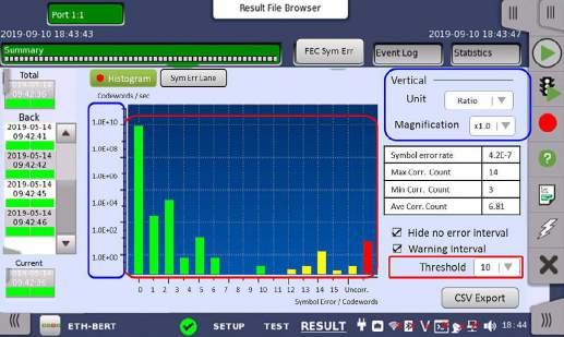
400G Ethernet FEC Analysis Ethernet equipment interfaces use optical modules. With some exceptions, pass/fail verification of optical modules up to 100G is performed simply by measuring the bit error rate (BER) for a fixed period of repeated sending and receiving of signals to confirm the error-free status. Similarly, network throughput and latency are measured using a BERT. However, the 400G Ethernet PMD layer is switching to PAM4 and FEC (Forward Error Correction) to correct errors occurring at optical transceivers and networks transmitting extremely fast signals, and to assure both communications quality and lower costs. FEC is a technology for correcting errors within the correctable range, and assures high reliability as well as extended transmission distance.
Service Activation Test (Y.1564).
This consist of service configuration and service performance test. These tests include • Color-aware and non-color-aware in combinations (IP DSCP or VLAN PCP) • Test modes: One-way (uni- or bi-directional, symmetrical or asymmetrical), Round-trip • Verification against service acceptance criteria: Information rate, Frame transfer delay, Frame delay variation, Frame loss rate, Availability Optional GPS timing synchronization All services tested simultaneously at CIR • Duration 15 min, 2 h, 24 h, user programmable • Results: Pass/Fail indication, IR (Min./Avg./Max.), FL (Count/ FLR), FTD, FDV (Min./Avg./Max./Current (during measurement)), AVAIL (%), Unavail (s).
Service Disruption Measurement. Service disruption measurement activated as part of BER test includes • Max./Avg. service disruption time, Resolution: 0.1 μs • Number of service disruptions • Disruption Type: Packet, LOS
Fibre Channel Test:
Installing the Fibre Channel option supports Fibre Channel tests from 1GFC to 16GFC. • Latency measurement • BER tests including service disruption measurement • Performance Test • Buffer Credit environment • Confirming optimum network parameter values
Anritsu Metro DC I&M Solutions
Anritsu's range of testers for resolving the above-described data center I&M issues includes the Network Master Pro MT1040A/MT1000A, Access Master MT9085series, and Fiber Maintenance Master MT9090A listed below.
Data Center I&M On-site Solutions
Network Master Pro (400G Tester) MT1040A Measurement Function Features Features
• Network screen 400G, 100G •Optical fiber evaluation OTDR, Optical Power Meter All-in-one support for tests from DCI optical fiber installation to 400G network circuits
Data Center I&M On-site Solutions Measurement Function Features Features
Network Master Pro (Ethernet/CPRI / OTDR Test Equipment) MT1000A • Network screen 10M, 25G, 100G •Optical fiber evaluation OTDR, Optical Power Meter All-in-one support for tests from DCI optical fiber installation to 100G network circuits Data Center I&M On-site Solutions Measurement Function Features Features
OTDR - ACCESS Master MT9085 Series • Optical fiber evaluation OTDR, Optical Power Meter DCI optical fiber evaluation Wide dynamic range for longdistance support
Data Center I&M On-site Solutions Measurement Function Features Features
µOTDR Module™ Series MT9090A •Optical fiber evaluation OTDR, Optical Power Meter DCI optical fiber evaluation Compact and lightweight with easy to use Fiber Visualizer
Key consideration in selection of testing tool
To assure and improve network quality, operators perform periodic equipment upgrades and maintenance, so they prefer measuring instruments with a variety of interfaces to help assure efficient work in the shortest time.
Here are some key points to consider when selecting any Data Centre Installation & Maintenance tool.

i) Data rates & interfaces: Any testing tool must have support of various data rates & interfaces used in todays industry. Below table shows some interface and supported technology.
ii) Easy to use GUI- Graphical Unser Interface (GUI). Tester must have very user-friendly GUI. This helps to reduce learning curve and expedite testing. This ensure Data Centre is performing well and SLA with customers are met.
iii) Automation in measurement process: Many times, field engineer/ technician is not well trained for proper usage/ testing of various test required during installation or maintenance of Data Centre. In such scenario trained engineer can easily configure test instrument to perform required test. Testing procedure is saved in instrument and just one button click is required to test. This helps to achieve better network efficiency & performance.
Traditionally, the operator creates a job ticket explaining the required tests to be completed with simple and clear stepby-step requirements for the technician running the tests. Commonly the job ticket is provided either as a paper hardcopy or PDF, this work procedure can now be registered in the
MT1000A/MT1040A using the free Scenario Edit Environment Kit MX100003A (SEEK) software for PC, with an intuitive GUI helping lighten the operators workload and ensuring all required testing is completed by the engineer. Automation supports creation of test scenarios without expertise in program language minimizing complexity and user error. Anritsu Corporation has announced strengthened Signal Quality Analyzer-R MP1900A PCI Express receiver tests. These strengthened functions upgrade the high-quality waveform performance of the PAM4 PPG MU196020A to the latest high-speed, large-capacity PCI Express standards for PCIe receiver tests. As a result, customers planning and developing PCIe Gen6 (PAM4 32 Gbaud) products for data centers and other applications now have an all-in-one measuring instrument covering future PCIe Gen6 upgrades as well as current PCIe 3.0/4.0/5.0 receiver tests. The Signal Quality Analyzer-R MP1900A series are multichannel bit error rate (BER) measuring instruments required for designing and inspecting next-generation network interfaces, such as 400 and 800GbE, as well as high-speed bus interfaces, such as PCI Express 4.0/5.0, USB3.2/4, Thunderbolt, etc. These added functions support early-stage development of PAM4 PCIe 6.0 equipment using the PAM4 PPG MU196020A with high-quality data output performance. Moreover, combined use with the existing SI ED MU195040A PCI solution supports PCIe 3.0/4.0/5.0 compliance tests as an all-in-one solution for PAM4 performance evaluations and compliance tests. These version upgrades add the following functions: • Equalizer Search function for easy PAM4 BER measurement using high-performance PAM4 ED MU196040B and Eye Contour functions for evaluating PAM4 signal Eye margin characteristics. • SAS3/4 and DP1.4 receiver tests using PPG/ED MU195020A/ MU195040A.

iv) Data storage/ sharing: Testing instrument must have enough storage of measurement data- trace and interfaces to transfer/ share this data for further analysis and reporting. v) All -in- One feature: Test instrument must be able to perform field and lab test, and multi-function, multi feature type so that CAPEX is limited i.e. cost saving. Anritsu Network Master Pro MT1040A supports lower to higher ( 10M to 400G) data rate, Ethernet, OTN test and OTDR test as well in single unit.
Fiber Connector inspection is also possible using Video Probe.
Rohde & Schwarz and VIAVI Collaborated to Improve their 5G NR and LTE

Rohde & Schwarz and VIAVI Solutions have confirmed their partnership by verifying their respective test equipment on correct implementation for 5G NR and LTE. This exchange between the two companies will help accelerate UE commercialization. The verification is based on the R&S CMX500 5G NR wideband radio communication tester by Rohde & Schwarz and the TM500 network tester for user equipment (UE) emulation by VIAVI. With the regular exchange between both companies’ development teams, the sharing of knowledge and experience provides a powerful collaboration that helps speed UE commercialization. Charl Cilliers, the Vice President of Engineering at VIAVI, says: “Time to market is the number one priority for our customers and the benefit of this co-operation is that we can accelerate our technical development to launch new 3GPP features at a much earlier stage. This helps our customers achieve their goals. One of the enablers of this cooperation is the 5G testing portfolio offered by Rohde & Schwarz, together with a wealth of experience in wireless technologies in both companies.” Christoph Pointner, Senior Vice President for Mobile Radio Testers at Rohde & Schwarz, comments, “Rohde & Schwarz is pleased to cooperate with VIAVI as a leading provider of network testing equipment. When two major T&M specialists combine their expertise in joint development, the results benefit both companies and also all their customers in the network and UE testing fields.”


Transforming How Infectious Diseases Are Detected Through Nanosensor Technology Diagnostics Analog Devices, Inc. (ADI)
What would it take to transform the detection, diagnosis, and surveillance of infectious disease worldwide, and develop a device that could produce accurate, reliable results, quickly?

Recent events surrounding the threat posed by the COVID-19 global pandemic highlight the urgent need for better methods for front-line mass screening to contain the spread of microbial pathogens. Today’s practice of scanning foreheads for signs of fever cannot detect asymptomatic or presymptomatic infections, nor can it distinguish the deadly novel coronavirus from less life-threatening respiratory illnesses. And other diagnostic test methods may be inaccurate or too slow to return results.
One pioneering biotech company envisioned a bold new solution, a breakthrough concept using portable nanosensor technology diagnostics to pinpoint pathogens in under one minute. But to commercialize its patented technology and bring its life-saving platform concept to market, it needed a strategic partner with deep domain knowledge and fabrication expertise. This would be realized through a partnership with the Analog Devices, Inc. (ADI) innovation center—the Analog Garage, and with ADI’s Hillview fab process engineering team.
Invaders Microbial pathogens, including viruses and bacteria, are responsible for millions of deaths a year. During the last century, the fight to control infectious disease met with numerous successes, including the eradication of smallpox, and the near elimination of measles, mumps, and tetanus. But viral epidemics and pandemics still occur, impacting the lives and economies of nations.
Transmission electron microscope image showing COVID-19 coronavirus emerging from the surface of human cells. (Image: © NIAID-RML)

Fighting Back
How can we keep people safe in the continuing battle to control and eliminate deadly contagions? Front-line mass screenings are one solution. However, current methods for detecting infectious disease in the field take 15 minutes to 4 hours—too slow to control the spread or contain a rapidly advancing pandemic. Furthermore, today’s tests are often inaccurate or expensive and require lab time, trained technicians, and complex sample preparation.
Current Diagnostics
• 15 minutes to 4 hours • Impractical for mass screenings


Mass Symptom Screenings Today
• Only look for fever and cough • Can’t detect cases without symptoms • Can’t distinguish between respiratory illnesses
A different type of coronavirus test is required to screen the U.S. population on the necessary scale. What is needed is a test that detects antigens, which would require a major technology breakthrough.


Pinpoint: A Breakthrough Change Agent
Pinpoint Science, a Northern California healthcare technology startup, envisioned a more effective solution for point of care testing and diagnostics—an easy- to- use, portable reader and plug-in cartridge, armed with an advanced nanosensor. As an agent for change, the device could quickly detect biomarkers, such as antibodies and antigens, and rapidly identify the specific microbial pathogens responsible for causing sickness and death. Equipped with disposable, targeted pathogen detection cartridges, the reader would generate precise results in the field, with no lab, medical technicians, or sample prep needed.
The science underlying Pinpoint’s nanosensor technology diagonostics was developed by Pinpoint’s Chief Scientist, Dr. Nader Pourmand, Professor of Biomolecular Engineering at UC Santa Cruz.
“We started a few years before COVID-19 emerged,” said Pinpoint CEO Lisa Diamond. “We were targeting influenza in humans and bluetongue virus in animals with a nanosensorbased test, a diagnostic using antibodies or synthetic molecules to detect and measure specific proteins to identify infection. We believe our platform will maintain its value to humanity well beyond the COVID-19 pandemic.” Today, Pinpoint is working to commercialize this technology, originally derived from functionalized nanopipettes developed by Dr. Nader Pourmand.

Pinpoint and ADI Join Forces
In early 2019, Pinpoint turned to Analog Devices, Inc. (ADI) and its innovation center, the Analog Garage to help transform its dream into a reality. The Garage, together with ADI’s Hillview fab process engineering team, partnered with Pinpoint to mature and bring to market its point-of-care rapid pathogen detection technology. Pinpoint Science selected ADI for its unique MEMS fabrication capabilities and sensor development capacity and its willingness to invest in emerging technology. ADI’s precision data converters are also a perfect fit for electrochemical platforms such as Pinpoint’s. Pinpoint’s portable reader will be based around one of these products – the ADuCM355 chemical sensing platform.

Early Evaluation Stage
ADI modified its process to custom fabricate the sensor based on the early-stage startup’s design. Pinpoint will do the testing to characterize the sensor’s performance, and if the results are positive, transform it into a functionalized nanoporebased biosensor. “Analog Devices believes Pinpoint’s novel nanosensor technology diagnostics holds great promise for a wide range of applications, especially for rapid, low cost pathogen detection, and we look forward to collaboration with Pinpoint in bringing this breakthrough technology to market,” said Nimrode Moreshet, director of emerging business, ADI.
Launching New Companies into the Unknown
ADI first discovered Pinpoint Science through SkyDeck, an early stage UC Berkeley incubator. Pinpoint Science was at SkyDeck for two terms, receiving formative guidance and support from the renowned academic accelerator. ADI was an early investor in SkyDeck–the global hub for entrepreneurship recognized for launching new companies into the world.
“Our collaboration means we can begin to realize the potential of our groundbreaking technology,” commented Lisa Diamond, CEO, Pinpoint Science. “We are still at an early stage. However, if our vision is confirmed in validation testing, we see the immediate real-world need for our platform, especially with the pandemic posed by the novel coronavirus. Pinpoint's technology holds the potential to address the urgent need for universal COVID-19 testing.”

Pinpoint’s Vision: Simple, Flexible, and Fast Pathogen Detection
Pinpoint’s vision is to create a general-purpose platform— swappable cartridges plug into a reader to detect specific pathogens in samples of blood, saliva, or nasal secretions. The cartridge’s nanosensors can detect specific markers of infectious disease: viral and bacterial proteins and host antibodies. Results are displayed in less than one minute.

Pinpoint’s novel biosensor technology makes label-free electrical detection of specific biomolecules possible, with high precision and low cost for applications such as point-ofcare diagnostics, pandemic screening, animal health, and food safety.
The Human Impact of Pinpoint’s Nanosensor Technology Diagnostics
Today, as the pandemic spreads across the world, Pinpoint Science is highly focused on COVID-19 virus detection. Significant technical risks and design challenges remain. But the trusted collaboration between Pinpoint and ADI brings the promise of reducing the time and cost of detecting infectious diseases globally while improving personalized patient care and saving lives.

We Stand By Our Commitment To Indian Market
With an in-house PCB designing, manufacturing unit and a corporate office indigenously designed, Laxmi Remote (India) Private Limited (LRIPL) is one of the oldest names when we all have these remote controls in our palms. With today’s dynamic changing digital world, Niloy from BISinfotech was eager to know the company’s never-forgotten journey, ahead plans, strategies and their unique offerings. Vijay Kumar Sachdeva, MD & CEO, Laxmi Remote (India) Private Limited (LRIPL) has the sheer prowess in understanding business which has made the company taste success for decades. The untold edited nub below.
and footprints across the country.
Laxmi Remote (India) Pvt. Ltd, a pioneer in remote control technology, is a leading manufacturer of remote controls, set-top boxes, adapters, power supply, mobile chargers & AV cables. The company formerly known as Remotec Industries was rebranded in the year 2000 as Laxmi Remote India Pvt. Ltd. Our trading business came to a halt in 1998 and we debuted into the remote control manufacturing industry. We opened our first manufacturing plant in Bahadurgarh, Uttar Pradesh in the year 2001, and by 2003, we had established our in-house PCB designing and manufacturing unit along with a corporate office in Noida, Uttar Pradesh. We established another manufacturing unit in Noida Phase II, in the year 2006, with a focus on manufacturing remote controls and set-top boxes for our business partners. After achieving tremendous success, we decided to further expand our portfolio by adding FTA set-top box and AV cables in our manufacturing capabilities to cater to the need of end consumers as well as businesses. In 2018, we established our R&D centre at Hyderabad with a more focused approach to drive innovation for setup box & software division. Laxmi Remote India has its own Conditional Access System (CAS)
An anecdote about Laxmi Remote (India) Private Limited (LRIPL)? Establishment, key offerings, business model
under the brand name of Pro CAS. We have spent the past 25 years working hard to build a challenging reputation and breakthrough innovations in operations and manufacturing. What differentiates us from other players is that we provide end-to-end solutions to our clients. Our round o'clock support, cost-effective technology and quality assurance make us the trusted OEM/ODM partners to our clients.
Make in India vowing a larger sentiment across the nation, LRIPL role to foster it further and how has been the company playing an instrumental role across the manufacturing sector in India.
With the changing world dynamics and the massive push from the Indian government to create an Atmanirbhar Bharat, India is looking at a big opportunity to be a global electronics manufacturing hub. India is our biggest market and with a focus on Government’s ‘Make in India’ initiative, we have decided to strengthen our position by bolstering local production and manufacturing of remote controls to more than three million per month. Laxmi Remote today has emerged as a leading Indian OEM, ODM & EMS player, bringing back a focus on boosting local manufacturing and add to the job opportunities in the market.

With a clientele of over 60 companies, LRIPL has partnered with big enterprises such as Daikin, Blue Star, Voltas, Havells, Orient Electric, Bajaj, Luminous, Livpure, Whirlpool, Lloyd, Amber, Usha, Halonix, Carrier Midea, Ricoh, SUN TV amongst others. The strong customer engagements and services have been a testimony to LRIPL’s 25 years of manufacturing excellence. With the ever-changing electronics manufacturing world, Laxmi Remote India is ready to meet the needs of the new normal through its advanced and sustainable infrastructure, capacity and manpower. We stand by our commitment to the Indian market and constantly challenge ourselves to deliver the best cost of ownership to our customers. As ‘Make in India’ campaign is making efforts by backing local firms and manufacturers to increase domestic manufacturing in the electronic sector, we will take hold of this opportunity and achieve greater success in our forthcoming endeavours.
Given the pandemic situation what shall be the company’s revenue target and strategies to achieve it?
We are planning to strengthen our facilities and targeting 20% production growth in the near future. In the next 5 years, we aim at becoming a 500 crore company while generating mass scale employment opportunities in the manufacturing and services sectors. With the vision to maximize India’s electronics manufacturing potential, we also aim to lead OEM remote control business.
Additionally, we are also considering the possibility of entering into LED TV manufacturing business with a manufacturing plant in the near future. Currently catering to 25% of the overall remote control manufacturing demands in India, we are working on technologies like Radio Frequency (RF), Touch Screen, and Voice Control along with Bluetooth technology in the category of remote controls. As the Consumer Electronics and Appliances Industry in India is expected to become the fifth-largest in the world by 2025, we are focusing more on the sectors like Medical, IoT, Consumer Electronics & appliances and working towards manufacturing electronic products to support these segments.
With advanced technologies (IoT, Predictive Maintenance) becoming a new cognizance across the EMS industry. How do you look into the change and impact of it in the business?
While the winds of change are favoring our country and major economies interested to invest in India, the domestic industry really needs to scale-up vertically and horizontally. This basically means that we need to size-up our capacities to manufacture quality electronic parts while various sectors need to invest strongly on research and development of trending and emerging technologies. Our factory and production lines will also adopt the latest technologies that will boost production volume and quality of products. There are several domains with strong emerging technologies such as IoT, Automation, 5G etc that can be the biggest demand creators for the electronics manufacturers. By capitalizing on the mentioned technologies, India is soon expected to consolidate its position as a major market leader in the world.
Vijay Sachdeva, you have been a known veteran across the EMS industry. How do you collar defining the strategic roadmap for the organization?
Being responsible for overall growth and development of the company, my main focus will be taking care of scaling up the venture, reinvent business processes, discovering new revenue streams, diversification, strategic alliances and balance risk and reward. At the forefront of the company’s growth, I support, formulate, and implement clear short-term and long-term operational and business strategies. I work closely with my production team to evaluate and ensure that we deliver the most effective production outcome for clients. There should be a right balance between being ‘customercentric’ and ‘employee-centric’ in order to benefit from and provide benefits to both. We are expecting the Indian market to bounce back as electronic manufacturing in India is expected to grow in the coming months, considering the new schemes and steps recently introduced by the government. We are more focused towards trending and emerging technologies for us to establish ourselves as the leader in electronics manufacturing and further bolstering LRIPL’s position as a global thought partner. We are going all out in building partnerships with enterprises and different industries and are putting insufficient time and investment into it.
Given the growing competitiveness, what factors are been kept of pivotal focus to explore new markets and drive holistic growth of the company?
Competition is good, in fact, a healthy competition always challenges you to work smarter and pushes you to offer better services, product quality and customer experience. Our focus has always been on quality, just-in-time delivery and reverse logistics. What differentiates us from our competitors is that we provide end-to-end solutions to our clients. Right from the development of moulds to building sophisticated cabinets, design & development of PCBs to assembly and to manufacturing the final products, after an appropriate stringent quality process, Laxmi Remote India controls the entire production process.
We are constantly working on new technologies and innovations that are approaching the market and training ourselves in order to stay on top of industry trends and opportunities. We keep on upgrading technologies and equipment to best utilise mankind, material and machines. We have built a well-diversified portfolio with time.
In today’s complex marketplace, a well-maintained portfolio is vital to any business’ success. Initially, we started with remote controls manufacturing and moved to the production of set-top boxes. We continued to invest a portion of our assets in other verticals and started producing adapters, power supplies and mobile chargers considering the growth of mobile phones and consumer durables in India. Going forward, we are also planning to expand our product portfolio by foraying into internet-based category products for the Broadcast & Cable industry such as IPTV, Hybrid Box, Android box & other products in the same categories.
Key markets (cities) in India that is strategically important for LRIPL’s business in 2020-2021?
We have established a strong foundation in India by bringing innovations and services for our clients. We have successfully maintained the right balance between our B2C and B2B businesses. Since customer satisfaction is the absolute core of our business, LRIPL is committed towards understanding their evolving requirement. Impacted by the covid-19 outbreak, we have taken major initiatives for adopting our manufacturing processes as per the new normal to facilitate our clients with their orders with us. We are executing all necessary provisions in manufacturing processes so that we don’t face any halt at any point of time and accomplish our clients’ orders and a
requirement on time. We cater not only to the local but also to global demands. With a strong pan India presence, we will continue to delight our customers and partners with our range of product line-up. We are proud to manufacture some of the cutting-edge products catering to varied segments, strengthening our portfolio and further consolidating our presence in the industry.
According to you, what are the major changes and trends you foresee in the industry?
The electronics manufacturing is yet to see its golden days in India. India’s manufacturing sector is expected to grow with a compound rate of 25-30% in the near future. The industry might witness a huge demand that will certainly shift the trend to automation processes and technology upgradation along with better infrastructural and logistical development. We can expect reform in medical electronics, consumer electronics, communication, broadband equipment and also defence electronics sooner. With a host of benefits they offer, IoT and AI technologies will also have a large role to play. Considering the same, the role of robotics in the manufacturing processes will be encouraged. As the government is focusing more on local manufacturing and rolling out different schemes, we can also think of developing infrastructure for components and other raw materials.
Lastly, what is the major challenge and way out you mull given the current EMS industry?
The dependency on China for components is still there and it will not go down soon. We need to develop an ecosystem for components. It is not possible to reduce dependency on China overnight. We need to take a comprehensive look at China’s innovative capacity. China has arguably the best technology infrastructure outside the western world. Backed by its technological dominance, Chinese software developers offer the best services not only technical but managerial too. The Chinese software companies and their cutting-edge technologies and revolutionary ideas are used by several industry giants. Anti-dumping duty on those Chinese manufactured goods which are already being made in India is extremely critical. We need a strict policy to tackle the presence of excessive under value import of raw material and other components.
Apart from components, the shortage of skilled workforce and advanced technology is also a challenge for the EMS industry where it is witnessing irregular demands. The higher cost of infrastructure, logistics inefficiencies and infrastructural bottlenecks, resulting in greater turnaround time and costs. These issues need to be addressed to further boost the growth of the EMS industry in India. In spite of all the above-mentioned concerns and with the help of appropriate industry initiatives and government interventions, electronics manufacturing is expected to rise in the future. Although the government has come up various schemes and initiatives such as ‘Make in India and Atmanirbhar Bharat’ to improve the business environment in the country, it further needs to set up a base which can scale up industries and facilitate ease of doing business in India. To further enhance the competitiveness of the Indian electronics manufacturing industry, these initiatives must be sustained with regular monitoring.


NEC, Analog Devices to Design 5G Massive MIMO Antenna Unit

NEC Corporation and Analog Devices have reported their collaboration to design a 5G Network Massive MIMO Antenna Radio Unit for Rakuten Mobile. The radio unit adopts ADI’s fourth-generation wideband RF transceiver solution to achieve high precision Massive MIMO and possesses a 5G open vRAN (virtual RAN) interface corresponding to Rakuten Mobile’s end-to-end fully virtualized cloud-native mobile network. It delivers large capacity transmission with high efficiency by using 3.7GHz frequency Massive MIMO and digital beam forming technology. NEC has already started shipping the 5G Network Massive MIMO Antenna Radio Unit to Rakuten Mobile. ADI’s fourth-generation wideband RF transceiver integrates quad-channel transmitters, receivers and Digital Pre-Distortion (DPD) in a single chip. The radio is fully software reconfigurable and covers all sub-6GHz 5G frequency bands, simplifying radio designs. NEC’s 5G equipment utilizes highly accurate digital beam forming for efficient high-capacity transmission. The system also features seamless installation, achieved through circuit integration.
ST Declares Third Quarter 2020 Financial Results
Updates
TDK Enhances New Power Inductors
TDK Corporation has formed new power inductors, BCL322515RT, for use in automotive electronics, intended for insertion into the power line of an automobile electronic control circuit. Using TDK’s proprietary material technologies and structure design, the inductors achieve high inductance (47 μH) in a small size (3.2 x 2.5 x 1.5 MM). The saturation current is 0.72 A. Also, by using metallic magnetic material as a core material, they were downsized by approximately 35% compared to products that used conventional ferrite material with similar attributes. The rated voltage is 40 V, and they can be used in a primary power supply circuit, which is input directly from an invehicle 12 V battery. The operating temperature range is from -55 to +155°C (including self-temperature rise), which supports severe temperature environments. Besides, the connection structure between the winding wire and the external electrode is designed to reduce open risks, ensuring high reliability. Recently, automobiles are increasingly likely to have an electronic control unit for information communication and self-driving, resulting in an increased number of inductors for power supply circuits used in the units. TDK will expand its lineup in the BCL series to meet a variety of customer needs year-over-year growth, with a double-digit operating margin
for power inductors to be used in automotive electronics, such as downsizing.
Main applications
• ADAS, a range of ECUs (Electronic Control Unit for automobiles)
Main features and benefits
• 47 μH achieved in a small size, decreasing inductors used • High reliability due to the product structure that reduced
STMicroelectronics has presented the U.S. GAAP financial results for the third quarter which ended on September 26, 2020. This press release also contains non-U.S. GAAP measures (see Appendix for additional information).
Jean-Marc Chery, STMicroelectronics President & CEO, commented “As we announced on October 1, 2020, our Q320 net revenues increased 27.8% sequentially, coming in 690 basis points above the high end of our outlook range. This revenue performance was due to significantly better than expected market conditions throughout the quarter. Demand for Automotive products, our engaged customer programs in Personal Electronics, as well as Microcontrollers, were the main factors that contributed to this result. The third-quarter gross margin came in at the mid-point of our range and includes about 140 basis points of un-saturation charges.”
“Looking at the fourth quarter, we expect sequential revenue growth of about 12.0% at the mid-point. All product groups are expected to grow, except for the RF Communications sub-group. Our gross margin is expected to be about 38.5%, including about 70 basis points of un-saturation charges.”
“For the full year 2020, we now expect net revenues at the mid-point to be about $9.97 billion, translating into 4.3% open risks
performance.”
ST reported third-quarter net revenues of $2.67 billion, gross margin of 36.0%, operating margin of 12.3%, and net income of $242 million or $0.26 diluted earnings per share.


Phase Change Materials: Innovations in Thermal Management
Jade Bridges Global Technical Support Manager & Ben Han Research and Development Engineer from Electrolube UK and China
Thermal Interface Materials (TIMs) are used in electronics applications to improve the efficiency of heat transfer and reduce the operating temperature of a device. They work by improving the conduction of heat through to a heat sink, where the heat is radiated to the surrounding environment by means of convection. Demand for improved thermal management in electronic devices is ever-increasing, particularly in applications where both miniaturisation and high performance are required in one package. A new generation of thermal Phase Change Materials (PCMs) have been developed by Ben Han of Electrolube China (Suzhou) providing practical and effective alternatives to more traditional thermal management solutions, such as non-curing thermal pastes or greases. A PCM is designed to alter its state at the phase change temperature, meaning that it will transition from a solid material to a softer, conformable interface above the phase change temperature. This allows the product to adapt to the contours of the surface, filling in all voids and small gaps, just like a paste would do on application, allowing for minimal bond line thickness and minimal thermal resistance at the interface.
Enhancing Heat Transfer
Typical applications that will benefit from enhanced heat transfer efficiency include technologies used in smaller electronic devices, such as mobile smart phones, gaming consoles, tablets, etc. These small devices perform many tasks at exceptional speeds and require increased power in order to do so. The size of the device means that the heat generated by the increase in power will have a negative effect on the performance and/or longevity of the device itself. Another significant area that relies on optimum thermal management includes power electronics, which are widely used in applications such as power distribution, sensor technology, electric vehicles and high-powered LEDs, to name just a few. Selecting the correct TIM for these applications is crucial to the long-term reliability of devices. The initial selection of suitable TIMs for testing is often conducted on the basis of high bulk thermal conductivity, indicating the efficiency of heat transfer through the TIM itself. However, bulk thermal conductivity alone, could give a false impression of the expected performance. When tests are conducted under application conditions, low thermal resistance of the device indicates the true heat transfer efficiency of the TIM and can be understood using the following formula: Total Thermal Resistance of a Device = (BLT/K) + Rc BLT = Bond Line Thickness of TIM K = Bulk Thermal Conductivity of TIM Rc = Total Thermal Contact Resistance at the Interfaces This formula proves that the bulk thermal conductivity is important but only in conjunction with the thickness of the TIM applied and the uniformity of the TIM across the interface surfaces. The formula also highlights why thermal pastes have continued to be a popular choice, offering good wetting of the contact surfaces for low contact resistance, whilst also offering minimal bond line thickness, addressing the surface roughness of the mating interfaces. However, PCMs have been introduced to provide similar performance to thermal pastes in these areas, whilst also improving on issues, such as the effects of pump-out and thermal stability over time.
The table below shows typical conductivity and resistance values of thermal pastes and gels, compared to PCMs, from
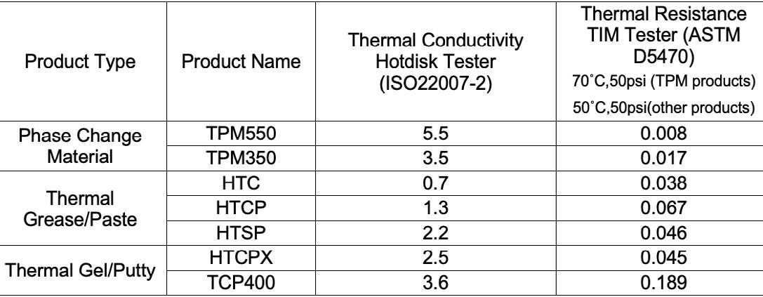
Electrolube’s thermal management range:
Pump-out
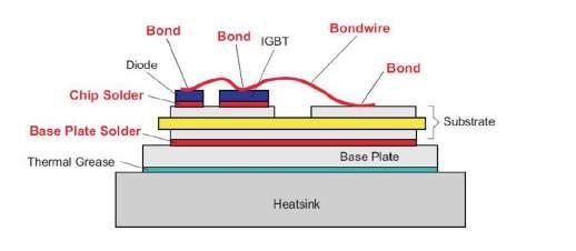
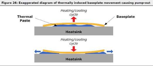
IGBTs are widely used in power electronics and provide a good example for understanding the effects of pump-out. They consist of a thermal stack, which includes materials of differing thermal expansion coefficients (CTEs) and a variety of bulk thermal conductivities, leading to temperature gradients
throughout the IGBT.
IGBTs and most devices in general will go through some form of thermal cycle, even if it’s as simple as switching the device on and off. When changes in temperature occur, all materials in the unit will expand or contract to a certain degree, depending upon the temperature the device reaches in operation and, ultimately, the temperatures that the individual components reach. The coefficient of thermal expansion will vary from component to component and so
contraction and expansion can happen at different rates, with adverse effects such as pump-out occurring as a result. When tackling issues with pump-out, it is important to understand the conditions and materials involved. Pump-out happens at the interface between mating substrates moving relative to one another during temperature changes. This results in a shear type action at the surface that can lead to changes in the rheology of the interface material and movement of that material from its original application position. PCMs alter their state above and below the phase-change temperature, so they are able to resist the effects of pump-out and remain more stable over many thermal cycles.
TPM550 – Thermal Resistance after Thermal Cycling Other testing
Power cycles also result in temperature changes of the device and in turn, the interface temperature. Powered devices also exhibit their own thermal cycle during use, which can be further exacerbated by external environmental conditions. Whatever the reason, thermal changes will result in some form of pump-out effect and so the stability of the chosen TIM under end-use conditions is critical to evaluate. As the application requirements govern the expected environmental conditions, it is typical to see a range of testing conducted in line with the application, rather than a standard set of conditions. Such testing is usually conducted within similar frameworks, illustrating the thermal stability of the
TIM after temperature cycling, high temperature bake and HAST (highly accelerated stress testing), and utilise thermal resistance values as an indication of stability. As can be seen from the graphs below, this accelerated testing provides a greater understanding of the lifetime of a TIM when compared to standard power cycle tests conducted under the exact
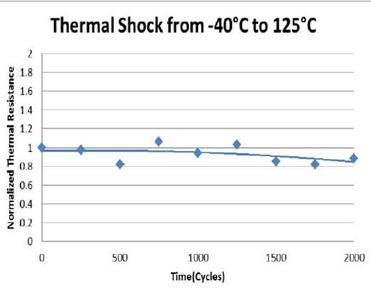
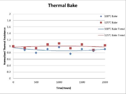

conditions of use.
The Importance of Stability
The stability of TIMs can be thought of as a visual test, simply put, has the product stayed in place following the test programme? If an interface material moves during a thermal test, either through pump-out or via the effects of gravity in a vertical orientation, it is likely that the performance of the product will also alter. Simple tests can include applying the product between two substrates and evaluating any movement or separation of the material during thermal shock testing. This easy test can highlight the importance of application of a thermal interface material, particularly in the case of thermal greases. These non-curing products are designed to be applied in thin films of around 50-100 microns but are often used at much higher thicknesses, which can result in
the pastes separating or moving relatively easily once the shearing action of pump-out occurs, and the overall efficiency of heat transfer is reduced. A phase change material is not affected in the same way by pump-out and shows greater physical stability than thermal greases.
In the wider context of TIM choice and material stability, it is important to mention what alternative approaches a user might consider. Electrolube has introduced some novel products that offer the benefits of traditional thermal management solutions while combining the stability required for high thermal cycling applications. These offer a surface cure only and form a stable compound that can be easily removed if rework is required. Other traditional products that provide a complete cure with a high level of stability include single-part silicones or two-part epoxies, however, rework is much more difficult with these products and they are unlikely to achieve the low thermal resistance of a traditional thermal paste.
Regardless of what the thermal interface material looks like after these tests, the most crucial point is if the thermal resistance at the interface has remained low and consistent, as this is the primary factor that is going to affect the performance of the device. PCMs have shown consistent thermal resistance when used as an interface material under a range of conditions, and are therefore chosen for their stability and capacity to maintain a low thermal resistance. But why do they perform so much better under these challenging conditions than a traditional thermal paste?
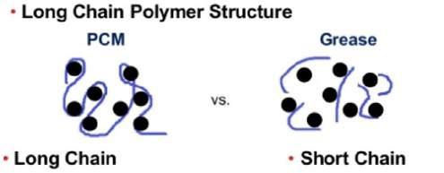
A phase change material alters its state from a solid to a softer material above a set temperature, usually around the 50˚C range. This function is achieved by using a polymeric material, rather than a base oil, as the basis of the TIM formulation. The polymer chains provide enhanced stability of thermal filler dispersion during both the solid and softened state. This results in enhanced thermal conductivity and long-term, low thermal resistances, as the material is kept in a more consistent state throughout its lifetime in the device. Thermal pastes on the other hand, are comprised of base oils with shorter molecular chains offering excellent wetting for initial application but possibly leading to issues including pump-out, drying out and oil bleeding over time.
Another important property of PCMs is their ability to store and release energy as the change of state occurs. This results in some thermal absorption and protects the device from sudden spikes in temperature due to rapid changes of power, for example. When considering which application is appropriate for a PCM, it is essential to have a proper understanding of the temperatures and temperature profiles that the device will be subjected to during operation. For example, while a device subject to thermal cycling or operation at a continually stable temperature will dictate what type of TIM is likely to achieve the most efficient performance, with PCMs there is the additional factor of the phase change temperature to consider. If the continuous operating temperature of the device is below the phase change temperature, the product will not perform at the level normally expected of it.
New Product Introductions
Electrolube recently added two new thermally conductive PCMs, TPM350 and TPM550, to its thermal management portfolio. TPM350 has a thermal conductivity of 3.5W/m.K and becomes workable at approximately 50°C. At this 'softening' temperature it changes state to become a more conformable material, minimizing thermal resistance at the interface and improving thermal transfer. Once it cools, it reverts back to its original state. The material’s advanced formulation ensures minimal contact thermal resistance.
TPM550 has a higher thermal conductivity of 5.5W/m.K and has a softening temperature of 45˚C. In common with TPM350, TPM550 produces no mess due to its thixotropic characteristics, which prevents flow outside of defined interfaces. Both PCMs can be reworked and more applications can be served per kilogram of the materials, reducing production costs.
These new PCMs are silicone-free, have an operating temperature range of -40 to +125˚C and are RoHS compliant. Both TPM350 and TPM550 are screen printable and, while they do contain small amounts of solvent to improve wettability on application, this rapidly evaporates following application to leave the solid phase change material on the substrate.
Conclusion
PCMs, once heated above their phase change temperature, become highly thixotropic liquids that perform as well as - and sometimes even better than – a traditional thermal grease. Moreover, their low phase change temperature ensures low thermal resistance over a wide temperature range, safeguarding minimal bond line thickness with improved stability and pump-out resistance. The application methods of PCMs for high volume production mean that most can be utilised in existing production processes with minimal, if any, changes, whilst also allowing for easy rework, offering many of the same benefits of traditional thermal pastes. As they offer greater long-term stability compared with thermal greases, they are better suited to thermally challenging applications where product life expectancy and reliability may be critical; such as automotive electronics or remotely located wind power inverters, for example. Traditional thermal pastes/ greases will continue to be a popular choice, although for some applications, especially those requiring greater longterm stability, a phase change material is likely to win over the crowd.
NOVEMBER 2020
Exploring the Possibilities With Proximity Sensors - OMRON Automation, India
The term "Proximity Sensor" indicates all those sensors that perform non-contact detection of target objects that are close by or within the general vicinity of the sensor, in comparison to other sensors, such as limit switches, that detect objects by physically contacting them. These Sensors convert information on the movement or presence of an object into an electrical signal.
There are three types of detection systems that do this conversion:
- systems that use the eddy currents that are generated in metallic sensing objects by electromagnetic induction, - systems that detect changes in electrical capacity when approaching the sensing object, and - systems that use magnets and reed switches.
OMRON Proximity Sensors are available in models using highfrequency oscillation to detect ferrous and non-ferrous metal objects and in capacitive models to detect non-metal objects. Models are available with environment resistance, heat resistance, resistance to chemicals, and resistance to water.
The portfolio comprises of the following categories :
- Rectangular : These Proximity Sensors use high-frequency oscillation. There are available in a wide range of sizes to enable selection to match the installation location. - Cylindrical : These Proximity Sensors use high-frequency oscillation. They resist heat, chemicals, and water better than Rectangular Sensors. They are available in both shielded and unshielded models. - Separate Amplifier : With these Proximity Sensors (highfrequency oscillation), the Amplifier and Sensor Head are separated to enable downsizing and facilitate adjustment. - Capacitive : Capacitive Proximity Sensors can be used to detect non-metal objects, such as liquids and plastics. - Others : Proximity Sensors are also available for special applications in long-distance models, and slim models are available for use combined with Proximity Sensors.ultrasonic
Features of Proximity Sensors
- No abrasion or damage to the object : The Proximity Sensors detect an object electrically without touching it, and so they do not cause abrasion or damage to the object. - Longer service life : No contacts are used for output. They use semiconductor outputs, so the Sensors have a longer service life (excluding sensors that use magnets). - Suitability for oil and water environments : Unlike optical detection methods, Proximity Sensors are suitable for use in locations where water or oil is used. Detection takes place with almost no effect from dirt, oil, or water on the object being detected. - High-speed resonance : They provide high-speed response, compared with switches that require physical contact. - Wide temperature range : They also find a great utility in a wide temperature range (from -40 to 200°C) - Not affected by colors: They detect the physical changes of an object, so they are almost completely unaffected by the object's surface color. - Affected by ambient conditions : Unlike switches, which rely on physical contact, Proximity Sensors are affected by ambient temperatures, surrounding objects, and other Sensors. Inductive and Capacitive Proximity Sensors are affected by interaction with other Sensors. Because of this, care must be taken when installing them to prevent mutual interference. Care must also be taken to prevent the effects of surrounding metallic objects on Inductive Proximity Sensors, and to prevent the effects of all surrounding objects on Capacitive Proximity Sensors.
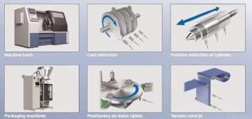
Industry segments utilizing the Proximity Sensors
Packaging, Machine Tools and Molding industries are the notable industries utilizing Proximity Sensors.
Symbolic Applications
- To detect the presence of cans during conveyance in order to prevent missing print with an ink-jet printer.
- To detect presence of a thin aluminum cap on water bottles

- To detect milk/juice inside a non-transparent white tetra pack.
How complex is design becoming with more and more connected devices getting its place in a chip. In an exclusive interview with Niloy from BIS, Harsha Jagadish, Pr. Engineer, Marketing, MCU16, Microchip Technology Inc. states as more and more devices are connected to the internet, the main cloud providers are encouraging usage of secure elements to secure private keys. Governments are also defining standards and upcoming legislation that will require the usage of a secure element. A lot more is known about IoT in semiconductors and lot more needs to be explored as the below nub wraps up the leader’s notion.
1. Microchip’s expertise in the IoT segment? Offerings, product portfolio and flagship offering.
As embedded applications continue to become more interconnected, requirements are increasing. The microcontroller, which is at the heart of any design, is required to be more flexible and offer the right level of intelligence. Adding communication must be simple, supporting a wide range of wired and wireless connectivity. With everything connected, secure connections become a universal need for all embedded applications. Whether they’re connecting to other systems, a smartphone or the cloud, these applications now require security to provide IP, brand and revenue protection. Microchip Technology provides total system solutions for smart, connected and secure IoT designs.

Our broad portfolio of PIC®, AVR® and SAM microcontrollers (MCUs), dsPIC® digital signal controllers and SAM microprocessors (MPUs) enable intelligence in IoT designs, while offering flexible peripherals and functions that let our customers differentiate their designs. Offering a range of wired and wireless connectivity solutions, either as part of the smart controllers or standalone devices, our connectivity solutions enable customers to add robust, reliable, high-speed connectivity and avoid getting stuck in the complex world of communication regulations by offering designs with certified modules.
With Microchip’s security expertise, our experts take the fear out of designing in security and remove the need for our customers to build costly in-house capabilities. From secure encryption to trusted execution environments, we enable security implementations that meet our customers’ unique needs with our wide range of security solutions, offering the right level of protection at the right price.
To accelerate design time, we offer our intuitive development environments, complete reference designs, free software libraries and automatic code generation tools to design IoT applications. Our IoT smart edge nodes, intelligent gateways and authentication solutions support many cloud platforms including Amazon Web Services, Google Cloud IoT Core and Microsoft Azure, and they also work with any on premise servers. This complete offering makes the development of IoT designs simple and enables our users to speed up their production and revenue stream.
2. Complexities arise with opportunities as IoT goes more mainstream. Trends, challenges and way outs Microchip has witnessed in this technology?
Security is the main concern, and it goes much deeper than just chip level security. It’s about practices. Security is as strong as its weakest link, and humans are just that. There is nothing drastically new to invent in embedded security practices, but there is all the knowledge from the decades of IT security to understand, learn, translate and apply to embedded systems. As more and more devices are connected to the internet, the main cloud providers are encouraging usage of secure elements to secure private keys. Governments are also defining standards and upcoming legislation that will require the usage of a secure element.
One of the main challenges in IoT security is how to address the paradox of customization, which is native in security due


