Optical Materials and Applications: Volume 1 Novel Optical Materials Francesco Simoni
Visit to download the full and correct content document: https://ebookmass.com/product/optical-materials-and-applications-volume-1-novel-opt ical-materials-francesco-simoni/
More products digital (pdf, epub, mobi) instant download maybe you interests ...
Optical Holography: Materials, Theory and Applications
Pierre-Alexandre Blanche
https://ebookmass.com/product/optical-holography-materialstheory-and-applications-pierre-alexandre-blanche/
Optical properties of materials and their applications
Second Edition Singh
https://ebookmass.com/product/optical-properties-of-materialsand-their-applications-second-edition-singh/
Optical Thin Films and Coatings 2e : From Materials to Applications. 2nd ed. Edition Flory
https://ebookmass.com/product/optical-thin-films-andcoatings-2e-from-materials-to-applications-2nd-ed-edition-flory/
Nanostructured Nonlinear Optical Materials: Formation and Characterization (Micro and Nano Technologies)
Rashid A. Ganeev
https://ebookmass.com/product/nanostructured-nonlinear-opticalmaterials-formation-and-characterization-micro-and-nanotechnologies-rashid-a-ganeev/
Ternary Quantum Dots: Synthesis, Properties, and Applications (Woodhead Publishing Series in Electronic and Optical Materials) 1st Edition Oluwatobi Samuel Oluwafemi
https://ebookmass.com/product/ternary-quantum-dots-synthesisproperties-and-applications-woodhead-publishing-series-inelectronic-and-optical-materials-1st-edition-oluwatobi-samueloluwafemi/
Spintronic 2D Materials: Fundamentals and Applications (Materials Today) Wenqing Liu (Editor)
https://ebookmass.com/product/spintronic-2d-materialsfundamentals-and-applications-materials-today-wenqing-liu-editor/
Solar Cells and Light Management: Materials, Strategies and Sustainability Francesco Enrichi (Editor)
https://ebookmass.com/product/solar-cells-and-light-managementmaterials-strategies-and-sustainability-francesco-enrichi-editor/
Biodegradable Materials and Their Applications
Inamuddin https://ebookmass.com/product/biodegradable-materials-and-theirapplications-inamuddin/
Optical Multidimensional Coherent Spectroscopy Hebin Li
https://ebookmass.com/product/optical-multidimensional-coherentspectroscopy-hebin-li/
Optical Materials and Applications - Volume 1
Novel Optical Materials Optical Materials and Applications Print ISSN: 3029-1089
Online ISSN: 3029-1038
Series Editor: Francesco Simoni (Università Politecnica Delle Marche, Italy)
Published:
Vol. 1 Novel Optical Materials edited by Iam Choon Khoo, Francesco Simoni and Cesare Umeton
Optical Materials and Applications - Volume 1
Novel Optical Materials editors Iam Choon Khoo The Pennsylvania State University, USA
Francesco Simoni Università Politecnica delle Marche, Italy
Cesare Umeton Università della Calabria, Italy
Published by
World Scientific Publishing Co. Pte. Ltd.
5 Toh Tuck Link, Singapore 596224
USA office: 27 Warren Street, Suite 401-402, Hackensack, NJ 07601
UK office: 57 Shelton Street, Covent Garden, London WC2H 9HE
Library of Congress Cataloging-in-Publication Data
Names: Khoo, Iam-Choon, editor. | Simoni, Francesco, editor. | Umeton, Cesare, editor.
Title: Novel optical materials / editors Iam Choon Khoo, the Pennsylvania State University, USA, Francesco Simoni, Università Politecnica delle Marche, Italy, Cesare Umeton, Università della Calabria, Italy.
Description: New Jersey : World Scientific, [2024] | Series: Optical materials and applications ; volume 1 | Includes bibliographical references and index.
Identifiers: LCCN 2023051524 (print) | LCCN 2023051525 (ebook) | ISBN 9789811280597 (hardcover) | ISBN 9789811280603 (ebook for institutions) | ISBN 9789811280610 (ebook for individuals)
Subjects: LCSH: Optical materials. | Optical materials--Technological innovations. Classification: LCC QC374 .N688 2024 (print) | LCC QC374 (ebook) | DDC 620.1/1295--dc23/eng/20231120
LC record available at https://lccn.loc.gov/2023051524
LC ebook record available at https://lccn.loc.gov/2023051525
British Library Cataloguing-in-Publication Data
A catalogue record for this book is available from the British Library.
Copyright © 2024 by World Scientific Publishing Co. Pte. Ltd.
All rights reserved. This book, or parts thereof, may not be reproduced in any form or by any means, electronic or mechanical, including photocopying, recording or any information storage and retrieval system now known or to be invented, without written permission from the publisher.
For photocopying of material in this volume, please pay a copying fee through the Copyright Clearance Center, Inc., 222 Rosewood Drive, Danvers, MA 01923, USA. In this case permission to photocopy is not required from the publisher.
For any available supplementary material, please visit https://www.worldscientific.com/worldscibooks/10.1142/13523#t=suppl
Typeset by Stallion Press
Email: enquiries@stallionpress.com
Printed in Singapore
c 2024WorldScientificPublishingCompany https://doi.org/10.1142/9789811280603 fmatter
Preface Thisbookisthefirstofanewseriestitled OpticalMaterialsand Applications thataimsatcoveringhottopicsinthewidelandscapeof researchrelatedtothisfield.Inthis series,abroadspectrumofmaterials willbeconsidered:fromsemiconductorstopolymersandliquidcrystals aswellasplasmonicandopticalmetamaterials.Applicationsmayspan frommicro-andnano-opticstoopticalinformationtechnology,optofluidics, biophotonics,imaging,holographictechnologies,andmore.Theaimofeach bookshouldbetopresentinacomprehensivewaythestate-of-the-artof thecoveredtopicinordertobeausefulreadforresearchersinthefield andforstudentsandscientistsapproachingitforthefirsttime.
Theseriesstartswiththiscollectionofchaptersthatisakindof miscellanea,samplesoftopicsthatmightbemoreextensivelypresented anddiscussedinsinglebooksoftheseries.
Thecollectionalsohasanotheraim:todisclosetheinspirationforthe newbookseries,whichcamefromthetopicsdiscussedintheconference “NovelOpticalMaterialsandApplications(NOMA).”Thismeeting,which hasbeenrecurringinItalyeveryalternateyearforoverthreedecades, providesaninternationalforumtodiscussthefundamentalsofthese materialsandtheirrolesinactual opticaldevices.Hence,beforethe chapterswepresentanintroductiondevotedtoabriefdescriptionofthe scientificandnon-scientificcharacteristicsofNOMA.
IamChoonKhoo FrancescoSimoni CesareUmeton
This page intentionally left blank
c 2024WorldScientificPublishingCompany https://doi.org/10.1142/9789811280603 fmatter
Preface v
Introduction:NOMA:ScientificandHumanUniqueness xiii
Chapter1.OpticalPropertiesandEmerging PhenomenaofTwo-DimensionalMaterials1 KunyanZhang,ArpitJain,WenjingWu, JeewanRanasinghe,ZiyangWang,andShengxiHuang
1Introductionto2DMaterials.................1
1.1Characteristicsof2Dmaterials.............2 1.2Examplesof2Dmaterials................3
2Fabricationof2DMaterialsandHeterostructures......4
Chapter2.OptothermalMarangoniEffect: PhenomenaandApplications31
AndrzejMiniewicz,StanislawBartkiewicz,MonikaBelej, KatarzynaGrze´skiewicz,andMichalina ´ Slemp
1Introduction...........................32
2PhysicsofMarangoniEffect..................33
2.1BriefhistoryofMarangonieffectanditsimpact...33
2.2SurfacetensionandMarangonieffects.........34
2.3Navier–Stokesandheattransferequations......37
3NumericalSimulationsandExperimentsonMarangoni Effectin2D...........................39
3.1Simple2DsimulationofthermocapillaryMarangoni effect...........................39
3.22DMarangonieffectsviewedexperimentally.....42
3.3Creationandmanipulationofgasbubbleswith optothermalMarangonieffect..............43
4ExperimentsonMarangoniEffectin3D...........48
4.1Dropletsandcrystalgrowthingasbubbles......48
4.2ManipulationofdropletsviaoptothermalMarangoni effect...........................50
4.3Marangoniswimmers..................52
4.43Dliquid-freesurfaceactuationbylaserbeam....57
4.5Hydrodynamictrap...................59
4.6Two-phaseliquidsystemsincludingliquidcrystals andpolymers.......................60
5ApplicationsofMarangoniEffect...............61
Chapter3.MolecularAlignmentPatterning EnabledbyNovelPhotopolymerizationwith StructuredLightanditsOpticalApplications71
SayuriHashimoto,KyoheiHisano,MihoAizawa, andAtsushiShishido
1Introduction...........................72
2ANovelConceptofPhotoalignmentMethodEnabledby MolecularDiffusion.......................75
3TheDetailedMechanismofMolecularAlignment bySWaP............................78
4VersatilityofPolymerizationSysteminSWaPforUniform MolecularandMesoscopicAlignment.............82 5Two-dimensionalAlignmentPatterninganditsPotential ApplicationstoOptics.....................86 6Conclusion...........................88 References..............................88
Chapter4.NonlinearOpticalPropagationin HeliconicalCholestericLiquidCrystals93 AshotH.GevorgyanandFrancescoSimoni
1Introduction...........................94 2ElectromagneticTreatmentofLightPropagation......97 3OpticalReorientationinChOH................100 4NonlinearLightPropagationatConstantIntensity.....104 5MultilayerApproach......................108 6Conclusions...........................116 References..............................118
Chapter5.LiquidCrystalsforDisplays, SmartWindows,TunableMetamaterials, PlasmonicNanostructures,Micro-ring Resonators,andUltrafastLaserManipulations121 I.C.KhooandT.-H.Lin
1Introduction...........................121
2OpticalPropertiesofLiquidCrystals—General Discussion............................123
2.1Molecularelectronicresponsestoopticalfields....124
2.2Linearopticalresponseandrefractiveindices.....125
2.3Nonlinearopticalresponsesandintensity-dependent refractiveindexchange.................126
2.4Electro-opticalresponsesofliquidcrystals—Abrief introduction.......................129
2.5Opticalpropertiesofchiralnematic[cholesteric] liquidcrystal—A1Dphotoniccrystal........131 3PhotonicsApplications.....................133
3.1Displaysandsmartwindows..............133
x Contents
3.2Tunablenear-zeroandnegativeindexofrefraction; metamaterialsandmetasurfaces............136
3.3Tunableplasmonicnanostructures,micro-ring resonators,enhancednonlinearity,andspontaneous emission..........................139
3.4Cholestericliquidcrystalsforpolarizationrotationof complexlaservectorfieldsandultrafast(ps-fs)laser pulsemodulation.....................141
References..............................146
Chapter6.Plasmonic-basedBiosensorsforthe RapidDetectionofHarmfulPathogens155
FrancescaPetronella,DariaStoia,YasaminZiai, FedericaZaccagnini,VivianaScognamiglio,DanaManiu, ChiaraRinoldi,MonicaFocsan,AminaAntonacci, FilippoPieriniandLucianoDeSio
1Introduction...........................156
2RefractometricBiosensors...................157
3SERS-basedTechniquesforPathogenDetection.......162
3.1SERS-basedplasmonic(nano)sensorsforbacteria detection.........................164
3.2SERS-basedplasmonic(nano)sensorsforvirus detection.........................170
4ElectrochemicalBiosensors..................172 5BiosensorsonFlexibleSubstrates...............176
5.1Electrospunnanofibers.................177
5.2Othersubstrates.....................180
6FuturePerspectives.......................181 Appendix:OpticalPropertiesofPlasmonicNanoparticles....182 Acknowledgments..........................185 References..............................185
Chapter7.ADoublePlasmonic/Photonic ApproachforMultilevelAnticounterfeit andFoodSafetyApplications195
AntonioDeLuca,VincenzoCaligiuri,AniketPatra, MariaP.DeSanto,AgostinoForestiero, GiuseppePapuzzo,DanteM.Aceti, GiuseppeE.Lio,andRiccardoBarberi
1Introduction...........................196
2TheDoublePlasmonic/PhotonicApproach.........200
2.1Thefirstphysicalunclonablefunctionlevel: Thechromaticsignature.................201
2.2Morphologicalandplasmoniccharacterizationof Agnano-islands.....................204
2.3Thesecondphysicalunclonablefunctionlevel: Thespectralsignature..................204
2.4Thethirdphysicalunclonablefunctionlevel: Themorphologicalsignature..............208
2.5Irreversiblethermalswitchinginthefieldof foodsafetyapplications.................212
3ExperimentalMethods.....................215
3.1AgandItosputteringdepositionparameters.....215
3.2Agnano-islandssputteringdeposition.........216
3.3CIE1931andCIELABcolorspaceanalysis......216
3.4EllispometricalandsmartphoneLEDflashlamp characterizationofthespectralresponseofMIN structures.........................216
3.5Temperaturevaryingellipsometry...........217
3.6Imagerecognitionalgorithm..............217
3.7Atomicforcemicroscopymeasurements........218 4Conclusions...........................218 References..............................219
Chapter8.Laser-AssistedMicromachiningand Applications225
L.Criante,R.Ramos-Garc´ıa,andS.Bonfadini
1Introduction...........................225
2FemtosecondLaserIrradiation:OutlineofTheory......228
3GlassMicro-chipFabrication.................232
3.1Selectivechemicaletching................232
3.2Femtosecondmicromachiningsetup..........235
4Needle-freeInjectorsina MicrofluidicPlatform: AChallengingApplicationfortheFLICEFabrication Technique............................237
4.1Thermocavitationbubblegeneration..........240
5Conclusions...........................245 References..............................246
Chapter9.NovelPhoto-sensitiveMaterialsfor MicroengineeringandEnergyHarvesting251 D.Sagnelli,A.Vestri,A.D’Avino,M.Rippa, V.Marchesano,F.Ratto,A.DeGirolamoDelMauro, F.Loffredo,F.Villani,G.Nenna,G.Ardila, P.Meneroud,J.Gauthier,S.Duc,M.Thomachot, F.Claeyssen,andL.Petti
1Introduction...........................252
2Photo-responsivePolymers..................255
2.1Mechanismsofphoto-responsiveness..........256
2.2Azobenzeneinphotomobilepolymers.........260
2.3Dopingofphotomobilepolymers............264
3MicroengineeringApplicationsofPhotomobile Materials............................267
3.1Introductiontomicroengineering............267
3.2Photo-responsivepropertiesinmicroengineering...269
3.3Applicationsofphotomobilematerialsinmicro valves,microswitches,andmicrosteering mirrors..........................273
4TowardPiezoelectricApplicationswithPhotomobile Materials............................283
4.1Introductiontothecombinationofpiezoelectric materialsandphotomobilepolymers..........283
4.2Photo-responsivepossiblearchitectureswith piezoelectrics.......................285
4.3Photomobilematerialsinenergyharvesting applications........................288
c 2024WorldScientificPublishingCompany
https://doi.org/10.1142/9789811280603 fmatter
Introduction:NOMA:Scientific andHumanUniqueness IamChoonKhoo∗,§ ,FrancescoSimoni†,¶ ,andCesareUmeton‡ ,
∗ PennsylvaniaStateUniversity,UniversityPark,PA,USA † Universit`aPolitecnicadelleMarche,Ancona,Italy ‡ Universit`adellaCalabria,Rende,Italy § ick1@psu.edu
¶ f.simoni@photomat.it umeton.fis@gmail.com
1.TheBeginning Theintendedyearofpublicationofthisbook,2023,coincideswiththe 16theditionoftheNovelOpticalMaterialsandApplications(NOMA) conference,whichwillbeheldfromJune4toJune9,2023,inCetraro— asmalltowninsouthernItaly,followingatraditionofmeetingevery alternateyear1 since1995.Actually,NOMAoriginatedfromthe“School onNonlinearOpticsandOpticalPhysics”2 , 3 organizedbytwoofus (I.C.KandF.S.)in1992inCapri(Italy),whichisdesignatedasthefirst edition.Thismeetingwasorganizedwiththefollowingingredients:(a) outstandinginvitedlecturerswithsp ecialtycoveringabroadrangeofnovel opticalmaterialsandtheirapplications;(b)limitedandselectednumberof participantsfromallovertheworld;(c)accommodationofallparticipants inthesamehoteloflimitedsizeinaremotebutidyllicsettingconducive forlocalizedinteraction.
1 Theeditionof2021wasshiftedto2022duetotheCOVID-19pandemic.
2 SeeKhoo,I.C.,Lam,J.F.,andSimoni,F.(Eds.). NonlinearOpticsandOptical Physics.Singapore:WorldScientific(1994).
3 SeealsoKhoo,I.C.,Simoni,F.,andUmeton,C.(Ed.). NovelOpticalMaterialsand Applications. NJ:Wiley(1997).
xiii
Thesefeaturesensurehighlevelofscientificinteractionsandexchanges inasecludedbutverypleasantenvironment,andthelimitednumberof participantsenablesthescientificexchangesanddiscussionstotakeplace duringtheentiredayspenttogetherinafriendlyatmosphere.Another importantingredientofNOMAisaffordability.Thecostofattendancehas beenkeptataminimallevelbyGrandHotelSanMichele,homeofNOMA since1995.Itwilltakeatreatisetoelaborateonthesespecial,arguably unique,featuresofNOMAandallthewonderfulhumanexperiences participantshaveappreciatedinthethreedecadessinceitsformation.We hopethatthefollowingbriefwritingscanconveywhatwehavecalled NOMAflavors—thespecialatmosphere,thesciencesandfriendships fostered,andthefondmemories.
2.TheLocation GrandHotelSanMicheleislocatedinCetraro,asmalltownonthe TyrrhenianSeapartoftheMediterraneaninthenorthsideofCalabria region,insouthernItaly.Appearingasabighousesurroundedbybeautiful treesandflowers,itisabouttwokilometersoutsidethetownonanice greenhillabout150mabovesealevel.Theborderofthehotelpropertyis arockycliff;anelevatorgoingdownthroughtherocksbringshotelguests toaprivatesecludedbeachandanopen-airrestaurant.
BesidestheMediterraneansecludedbeachforswimmingandoutdoor dining,thehotelfeaturesmanyfacilitiesincludingalarge,fullyfunctional conferencehall,golfcourse,vineyard andcellar,swimmingpool,tennis court,bars,andrestaurants.Itusuallyprovidesfullboardtothehotel guests,startingwithaverypleasantbreakfastontheterraceorveranda. Itoffersmanyseats,sofas,andsmalltablesbothindoorsandoutdoorsfor gueststotalk,work,orhaveadrinktogether.Duringthe conference,lunch isusuallyheldatthebeachterracerestaurant,afamilyplacewithtypical Mediterraneanarchitectureprovidingacongenialatmosphere.Ofcourse, beinginItaly,maximumemphasisisplacedonthequalityand“quantity” ofthefood,withsometypicaldishesoftheCalabriaregion.
Alltheseamazingfeaturesarestrengthenedbythegreathospitality extendedbytheworkingpersonnelandtheowner,keepingthehotel guestscomfortablewiththeirkindandfamilialattitude.Thankstothe prestigeofthesponsoringandcooperatingSocietiesandtotheeffortsand connectionsinvolvingalsotheDepartmentofPhysicsoftheUniversity
ofCalabriaandtheAdministrationoftheGrandHotelSanMichele, thesewonderfulexperiencescomeat verylowcost,andensurethatall meetingparticipantsratherstayonsiteafterthemeetingsessions—the fundamentalrequirementtocreatetherightsocialenvironmentforfruitful scientificexchangesandrelaxations.
Afurtheropportunityforsocializationisrepresentedbythecultural trip.Conferenceattendeesareofferedthepossibilityofspendingonedayof “fullimmersion”intheCalabrianculturaltradition,withvisitstocastles, ancientvillages,archaeologicalexcavationsofMagnaGraecia,museums, andcenturies-oldpineforests,withlunchesinhigh-levelgastronomic restaurantswheretypicaldishesoftheCalabrianculinarytraditionare offeredinalandscapeofenchantingbeauty.
3.ScientificExcellence ThefocusoftheNOMAmeetingseriesisonnovelopticalmaterialsthat possessuniquecharacteristicsforapplicationinnonlinear-andelectrooptics,communications,sensing,integrated-,nano-,andbio-photonics/ phononics.2,3 Needlesstosay,inthelast3decadessinceitsformation, opticalmaterialsofinteresthaveevolvedfrommanyconventionaltypes tonewemergentones,andparticipants,whilelimitedinnumbers,include manyworld-leadingexpertsinwiderangingandrapidlydevelopingoptical andphotonicsciences.NOMAisintendedtobeinternationalincoverage, andparticipantscomefromallthecountriesofEurope,theAmericas,Asia, andAustralia.
EveryeditionoftheNOMAMeetingshasbenefittedfrommany outstandingspeakersoncurrenthottopicsinthebroadfieldof Optical MaterialsandApplications,includingthelateProf.NicolasBloembergen (NobelPhysicsLaureate,1981)—thePlenaryspeakerinthefirstNOMA heldintheGrandHotelSt.Michele,followedbyA.Yariv,E.Garmire, O.Svelto,C.Flytzanis,H.Eichler,T.Ikeda,E.Hanamura,R.Boyd, C.Tang,andmanyotheroutstandingscientists.Wewouldliketopay specialtributestoseveralcolleagueswhohavepassedawaysince:F.T. Arecchi,V.Degiogio,H.Gibbs,A.Kaplan,G.Stegeman,fortheirfrequent participationandcontributiontothetechnicalexcellenceofNOMA.
Thestronginternationalcharacteristestifiedbytheaverageparticipationof80/100scientists(including60/70speakers)comingfrom20/25 differentcountries.
AnotheringredientthatmakeseachNOMAMeetinguniquefromthe scientificpointofviewisthatwhileitisatopicalmeeting“atlarge,” itactuallydoesfunctionasmorecomprehensive.Usually,apersonparticipatesinatopicalconferencefocusedonaparticulartopicofhis/her ownexpertiseorinahugegeneralconferencecomprisingmanytopical subconferencesamongthousandsofattendees.Theresultisthatinany givencase,rarelyisoneabletohearsomethingnotrelatedtohiswork,and evenwhenthisispossible(e.g.,atsomeplenarysessionofbigconferences) itisdifficulttohaveanymeaningfulscientificexchangewithspeakersina differentfield.ThislimitationisovercomeatNOMAMeetingswhereina smallenvironmentitispossibletofollowspeechesonquitedifferenttopics, andthishastheadvantagesofmakingpossiblethescientificexchanges betweenscientistsworkingindifferentareas,andpossiblyforcreatingnew ideasforeachoftheparticipants’ownresearchinahighlyinternational scientificenvironment.
Inaspanofnearlythreedecades,materialsciencesandopticalphysics haveevolvedasdramaticallyasotheraspectsoflife,withoncehottopics beingreplacedbyemergentoneseverysooften,whilemanyhavewithstood thepassageoftimeandhavebecometextbookmaterials.
ThefollowingisapartiallistoftopicscoveredbyNOMAspeakersin recentyears:
Nanostructures
Metamaterials
Metasurfaces
NonlinearOptics
Nonlineardynamics
Biosensing
Biophotonics
Biomaterials
Liquidcrystals
Nanomaterials
Holographicmaterials
SmartMaterials
Photo-sensitiveMaterials
Light–MatterInteraction
PhotonicCrystals
Semiconductors
OpticalStorage
Nanooptics
OrganicMaterial
Plasmonics
OpticalManipulation
OpticalTweezers
Photo-mobilematerials
Optofluidics
SilkOptics
2-Dmaterials
TopologyPhotonics
This page intentionally left blank
c 2024WorldScientificPublishingCompany
https://doi.org/10.1142/9789811280603 0001
Chapter1 OpticalPropertiesand EmergingPhenomenaof Two-DimensionalMaterials KunyanZhang∗ ,ArpitJain† ,WenjingWu∗ ,JeewanRanasinghe∗ , ZiyangWang∗ ,andShengxiHuang∗,‡
∗ RiceUniversity,Houston,TX77005,USA † PennsylvaniaStateUniversity,UniversityPark,PA16802,USA ‡ shengxi.huang@rice.edu
Two-dimensional(2D)materialshaveattractedagreatamountofinterest becauseoftheirnovelopticalpropertiesinducedbythereduceddimension. Inthischapter,wediscussdifferenttypesof2Dmaterialsandtherelated fabricationtechniquesforproducing2Dmonolayersandheterostructures.The obtained2Dmaterialshostextremelystronglight–matterinteractionbecause oftheweakdielectricscreening.Inadditiontothefundamentalproperties,they demonstrateintriguingopticalphenomenasuchasmoir´eexciton,singlephoton emission,andhybridpolaritons.Theuniqueopticalpropertiesandtunable surfaceadsorptionof2Dmaterialscontributetoapplicationssuchasoptical modulation,quantumoptics,andbiologicalsensing.Thevastpotentialof2D materialscanbefurtherexploredwiththeaidofadvancedmachine-learning models.
1.Introductionto2DMaterials Ahalf-centuryago,RichardFeynmanbroughtuptheideaoflayered materialsduringhisfamouslecture.1
There’splentyofroomatthebottom.byasking, Whatcouldwedo withlayeredstructureswithjusttherightlayers ?Withdecadesofefforts, scientistsmaynowbeabletoanswerFeynman’squestion,thankstotwodimensional(2D)materialresearch.
K.Zhangetal.
2DvanderWaalsmaterialreferstoafamilyofmaterialswithstrongly bonded2DlayersattachedbyweakvanderWaalsforces.2 Individual layerscanbeeasilyseparatedbybreakingthevanderWaalsbonds.The firstsuccessfulisolationofsingle-layergraphenebackin20043 hasbrought 2Dmaterialsunderthespotlight.Overthepasttwodecades,tremendous effortshavebeendevotedbythescientificcommunitytoexploringthenovel physicsandapplicationsofsuchmaterials.
1.1. Characteristicsof2Dmaterials Comparedtotheirparentalbulkcounterparts,2Dmaterialsprocessdistinctivephysicalpropertiesowingtotheiratomicallythinnature.Theelectronic bandstructureof2Dmaterialsstronglydependsonthelayerthickness.For example,monolayerMoS2 becomesadirectbandgapsemiconductor,while thebulkMoS2 hasanindirectbandgap.4 Thisenablesanewwayofbandgap engineeringviathicknesscontrol.
Theelectricalandopticalpropertiesof2Dsemiconductormonolayers arealsodominatedbyexcitoniceffects.5 , 6 Thankstotheweakdielectric screeningandstrongchargeconfinementwithinthereduceddimension, anultra-strongCoulombinteractionemerges,givingrisetointriguing many-bodyphenomenainsuchmaterialsystems.Chargecarriersare tightlyboundedwithinoracrossthelayersaselectron–holepairs,called excitons.Excitonsandtheirhigher-ordercomplexes(trion,biexciton, hexciton,etc.)havebeenobservedinfew-layer2Dsemiconductorsandtheir heterostructures.Thereduceddielectricscreeningofthesub-nanometer layersresultsinthehighsensitivityofthelocalenvironmenttofactors suchasstrain,defects,andtemperaturechanges.7 –10 Electronsandholes canbetrappedinlocalpotentialwells,r esultinginlocalizedexcitons.Those trappedexcitonscaneitherbecomepronouncedquantumemissionsources or,incontrast,quenchtheintrinsicphotoluminescenceemission.
Themeritofan“all-surface”crystalstructuremakes2Dmaterials highlyfavorableforsurface-relatedapplications.Theyhavebeenwidely studiedforelectrocatalysisandsensingpurposes,suchashydrogen/oxygen evolutionreaction(HER/OER)11 anddiseasedetection,12 respectively. Furthermore,theatomicthicknesstogetherwithhighin-planestiffness provides2Dmaterialswithextremelyflexiblemechanicalproperties.
Moreexcitingly,thoselayered2Dsheetshaveconsiderablefreedomin layer-by-layerintegration,creatingadiversityofheterostructureswithout theconstraintsoflatticemismatching.13 Thismeritofferstheopportunity
OpticalPropertiesandEmergingPhenomenaofTwo-DimensionalMaterials 3 todesignandrealizenewmaterialplatformswithdesiredproperties. Theeasy-to-integratenaturealsomakesthempromisingforthefabrication offlexibleandcompactelectronic/optoelectronicdevices.
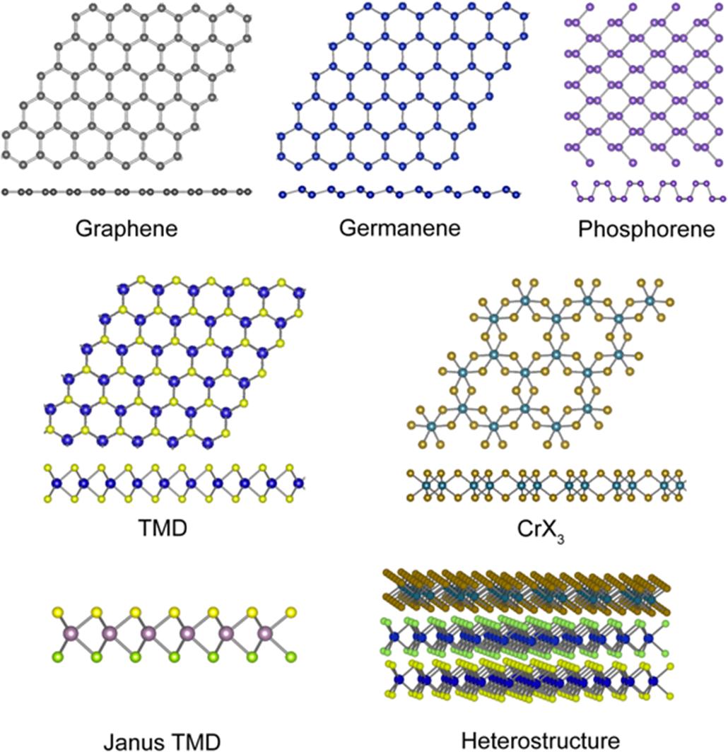
1.2. Examplesof2Dmaterials Asoftoday,alargevarietyof2DmaterialshavebeendiscoveredandinvestigatedassummarizedinFig.1.Thislargefamilyofmaterialscanbecategorizedaselementalmaterialslikegraphene,compoundmaterialslikeboron nitride,andstructure-engineeredmaterials,includingheterostructures.
Elemental2Dmaterialshaveattractedconsiderableattention,despite theirchemicalsimplicity.14 Thereexistsomeelemental2Dmaterialsthat
(a)
(b)
(c)
Figure1.Examplesof2Dmaterials.(a)Crystalstructuresofelemental2Dmaterials(topviewandsideview);(b)Twocompound2Dmaterials:TMDandCrX3 (X:I,Br);(c)Structure-engineeredmaterialslikeJanusTMDandartificiallyassembled heterostructures.
havetheirbulkforminnature,suchasgrapheneandphosphorene. Grapheneisasinglelayerexfoliatedfromgraphiteanditiscomposedofa honeycomblatticeof sp2 -hybridizedcarbon.15 Ithasazero-gapelectronic bandstructurewithlineardispersion.Phosphoreneisthemonolayerform ofphosphorus,exhibitinganorthorhombiclayeredstructurewithlayers bucklingoutoftheplane.16 Itshighlyanisotropicphysicalpropertiescome fromthisstructure.Manyothersyntheticelemental2Dmaterialshave beenexperimentallyachieved,17 includingborophene(B),18 silicene(Si),19 germanene(Ge),20 stanine(Sn),21 and2Dtellurium(Te).22
Compound2Dmaterialscanbefurtherclassifiedintomanycategories. Amongthem,transitionmetaldichalcogenides(TMDs)offerawiderangeof electronicproperties,fromsemiconductorstosuperconductors.23 SemiconductingTMDs,includingMoS2 andWSe2 ,havebeenexclusivelystudied formeritslikestronglight–matterinteraction,24 nonlinearpropertiesfrom brokeninversionsymmetry,25 strongspin-orbitcoupling,26 etc.Some metallicTMDshavebeenproventohostintriguingphysicalphenomena likechargedensitywave(CDW)27 andsuperconductivity28 undercertain conditions.Anothergroupofcompound2Dlayeredmaterialshasrecently gainedalotofinterest.Thesemateria lsincludetransitionmetalhalides (CrI3 ,CrBr3 ),Cr2 Ge2 Te6 ,andXPS3 (X:Ni,Mn,Fe).Magnetismispresent inthesematerialsevenatthemonolayerlimit.29
Structureengineeringofcrystalsemergesasanefficientpathwayto modifyandachievedesirednovelproperties.Oneexcitingexampleof structure-engineered2DmaterialsisJanusTMDs,30 whichhavedifferent atomicspeciesontheirupperandlowerfacets.Thissymmetrybreaking inducestheformationofanout-of-planeelectricdipole,whichiscapable oftuningtheinterlayercoupling.30 , 31 BuildingnovelvanderWaalsheterostructuresbyintegrating2Dlayers laterallyorverticallyprovidesaccess toprogrammablepropertiesbeyondtheirbuildingblocks.Whenstacking layerswithafinitetwistangle,amoir´eenergylandscapecanbecreated, resultinginaplethoraofeffectivelow-energyquantumHamiltoniansand furtherleadingtotherealizationofmanycorrelatedphases.32
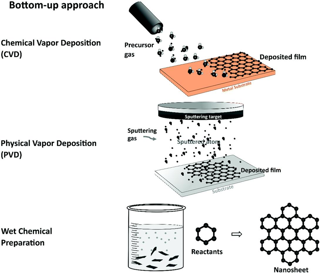
2.Fabricationof2DMaterialsand Heterostructures Variousbottom-upandtop-downsynthesismethodshavebeendeveloped for2Dmaterials.Forexample,vapor-basedsynthesismethodshaveenabled thewafer-scalesynthesisof2Dmaterialsforoptoelectronicapplications
5 andelectronicdevices.33 Chemicalvapordeposition(CVD)involvesusing metal-organicprecursorslikeMo(CO)6 ,chalcogenprecursorslikeH2 S,and acarriergaslikeAr/H2 .Thegasesenteratubefurnaceataspecifictemperature(200–1,100◦C)andpressure(1–760Torr),dissociate,andreacton thesubstrateplaceddownstreamtoformmonotoafewlayersofTMDs.34 IncontrasttoCVDsynthesisatrelativelyhightemperatures,substituting thetopsurfaceatomsofTMDmonolayersatroomtemperaturecan produceJanusTMDmonolayerswithbrokenmirrorsymmetry.35 Powder vaporizationisalsoverysimilarbutinvolvesusingpowderprecursorskept insidethetubefurnaceduringgrowth,leadingtoalossofprecisecontrol overtheprecursoramounts.Metaltransformationinvolvesdepositingthin filmsofeithertransitionmetalsorchalcogenprecursorsandsubsequent heattreatmenttoconvertthemto2DTMDs.
Additionalepitaxialgrowthtechniquesincludemolecularbeamepitaxy andatomiclayerdeposition,whichareimportantinspecificapplications andforunderstandingtheprecursor-substratechemistriesnecessaryfor CVDgrowth.GraphenecanbegrownepitaxiallyonSiCsubstratesby sublimingitathightemperatureswithlayercontroldependingonannealing time.36 Hydrogenatingthisstructurecanleadtotheformationofquasifreestandingepitaxialgraphene,whichshows2Delectrongasproperties andisanexcellenttemplateforepitaxialgrowthofhBN,37 GaN,38 and elemental2Dmetals.39 Chemicalvaportransportisanessentialtechnique forbulkcrystalformationforexfoliationpurposesandutilizesahalogen transportagenttogrowcentimeter-scalebulkcrystals.Thesetechniques arehighlightedinFig.2.
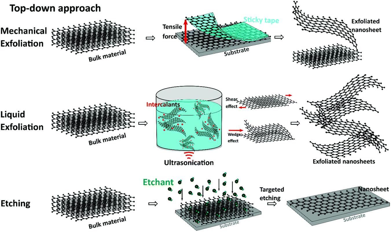
Exfoliationisalsoapromisingmethodusedtofabricate2Dmaterials (Fig.3).Asthenameimplies,itinvolvesremovingoneorafewvander Waalsbondedlayersfromabulksinglecrystalemployinganexfoliating medium.3 Inthecaseofmechanicalexfoliation,theexfoliatingmediumis atapethatisrepeatedlypeeledtoreducethethicknessof2Dmaterials. Graphene,oneofthefirst2Dmaterialstobediscovered,wassynthesized usingthetapeexfoliationmethodbyGeimandhiscoworkersin2004.3 Inliquidphaseexfoliation,asolventcanbeusedasanexfoliationmedium thatenterstheinterlayerspacesin2Dmaterialschemically(oxidativeliquid exfoliation)orthroughultrasonication,resultinginlarge-areaexfoliationof 2Dmaterials.40 Inaddition,large-areaexfoliationthatinvolvestheuseof thinmetalfilmsdepositedonbulk2Dcrystalcanalsoexfoliatemillimeterscalemonotoafewlayersof2Dmaterialsandtransferthemtothe substrateofourchoosing.41 2Dmaterialscanalsobepreciselythinned
Figure2.Primarybottom-upsynthesistechniquesfor2Dmaterials.Adaptedwith permissionfromRef.17 c 2020RoyalSocietyofChemistry.
Figure3.Primarytop-downsynthesistechniquesfor2Dmaterials.Adaptedwith permissionfromRef.17 c 2020RoyalSocietyofChemistry.
OpticalPropertiesandEmergingPhenomenaofTwo-DimensionalMaterials 7 downusinglaseretchingtoyieldselectiveanddamage-freelayercontrol.42 Theobtained2Dlayerscanbestackedontopofeachothertocreatevander Waalsheterostructurethroughpolymer-assisteddeterministictransfer.43 ApolymerstamplikePolydimethylsiloxane/Polycarbonate(PDMS/PC) isusedtopickupthedesired2Dmaterialflakefromthesubstrateand thendropitontoanother2Dmaterialflaketocreatetheheterostructure. Thisprocesscanberepeatedtoachievemultiple-layerstacks.Researchers havealsodevelopedautonomousmachineswhichcanexfoliate,identify, andcharacterizethe2Dmaterialsandcorrespondinglycreatetheirvander Waalstacks,allinsideaglovebox.44 , 45
3.OpticalPropertiesof2DMaterials Two-dimensionalmaterialspossessnovelopticalpropertiesduetotheir reduceddimensionality,uniqueelectronicstructure,anddielectricscreening.Theiruniquepropertiescanbeutilizedinnext-generationflexibleoptoelectronicdevices.Inthissection,wewilldiscusssomeofthefundamental opticalpropertiesof2Dmaterials.
3.1. Lightabsorption Eventhough2Dmaterialmonolayersarelessthanonenanometerthick, theyareexcellentlightabsorberscomparedtobulkcrystals.46 Absorbance inthesematerialscanbemeasuredusingdifferentialreflectanceortransmittancemeasurementsandcanalsobeinferredfromtheirdielectric constants.12 Forexample,theelectronicstructureofgrapheneisanalogous toalinearDiracconeattheFermienergylevel.Theopticalresponseof grapheneisdefinedbyinterbandtransitionsoccurringbetweenthevalence andconductionbands.Ithasbeenshownthatforpristinemonolayer graphene,itsopticalconductanceisdefinedonlybyuniversalconstantsand isindependentoffrequencygivenby σ (ω )= πe2 /2h. 47 Thecorresponding absorbanceisgivenby A(ω )=(4π/c)σ (ω )= πα,where α isthefine structureconstant.Thisleadstoatheoreticallypredictedabsorption valueof2.29%forgrapheneinthevisiblerange,whichisverysimilar totheexperimentallyobservedvalueof2.3%.47 , 48 However,thereare somedispersionsintheexperimentallyobservedabsorptiondatadueto deviationfromthelinearDiracconeofgraphene.48 Transmittancespectra formultilayergrapheneshowthereductionintransmittancebyafactor of πα foreveryadditionallayerofgrapheneuptofivelayersintotal.48 GraphenecanalsobeelectrostaticallydopedbygatingtoshiftitsFermi
levelandcorrespondinglychangetheinterbandabsorption,therebyleading tothetunabilityofitsopticalresponse.
TMDmonolayersarealsoexcellentabsorbersoflight,achievingabout 5–10%absorptionofincidentlightinthevisiblerange,46 whichisaboutten timeshigherthanthatofGaAs.Theirhighabsorptioncanbeexplained bythedipoletransitionswithalargedensityofstatesandoscillator strengthsbetweenlocalized d stateswithstrongspatialoverlaponthe groupVItransitionmetalatoms.46 ExcitoniceffectsinTMDsleadtoa highlyconstructivesuperpositionoftheoscillatorstrengthsneartheonset oftheabsorptionedge,49 whichhasbeenutilizedtocreatephotovoltaic devicesusingthesematerials.
3.2. Excitons MonolayerMoS2 isadirectgapsemiconductorwithabandgapofabout 1.8eV,50 makingitidealforoptoelectronicapplications.WhenMoS2 absorbsaphoton,anelectronleavesthevalencebandfortheconduction band,leavingbehindapositivelychargedholeinthevalenceband.This holeisstronglybondedtotheelectronbyCoulombicforcesandiscalled anexciton,aneutralquasiparticle.Iftheexcitonalsohasanassociated charge,itiscalledatrion.2DTMDsareuniquebecauseofhighlystable excitonswithsizeablebindingenergy,whichexistevenatroomtemperature duetotheirreduceddimensionalityandlowdielectricscreening.These excitonscanalsobeconvertedtophotonsandcanbeeasilymeasuredusing temperature-dependentphotoluminescencespectroscopy.51
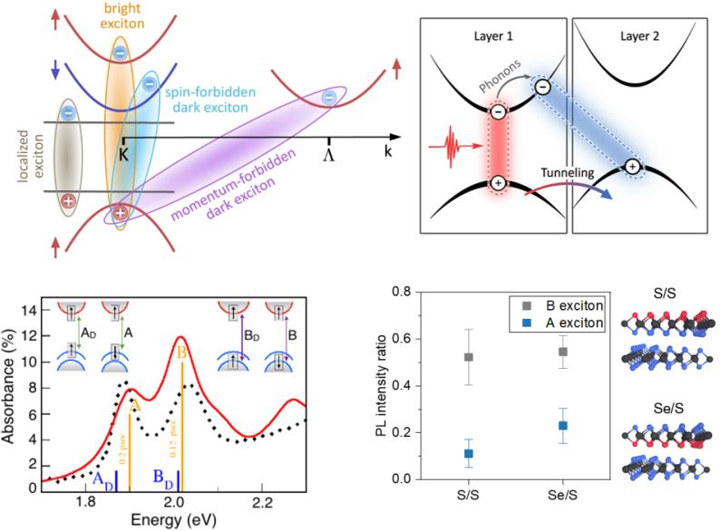
Figure4(a)describesthevarioustypesofexcitonswhichcanexistin a2DTMDmaterial.52 Brightexcitons consistofbondedelectronsand holeswiththesamespinandpositioninmomentumspace.Momentumforbiddendarkexcitonsconsistofbondedelectronsandholeswiththe samespinbutdifferentmomentumspacepositions.Spin-forbiddendark excitonsconsistofbondedelectronsandholeswiththeoppositespinbutthe samemomentumspace.Localizedexcitonsoccurdue toelectron–holepairs trappedinadefect-inducedpotential. Therefore,defectengineeringcanbe usedtomanipulatetheexcitondynamicin2Dmonolayers.53 Figure4(b) describesinterlayerexcitonsinheterolayersinwhichtheelectronsare presentintheconductionbandofonematerialandholesinthevalence bandofanother.
Excitonicbindingenergyisdefinedasthedifferencebetweenthe bandgapenergy(E0 )andtheenergyoftheobservedexcitonictransition (Ex ).52 ForMoSe2 , E0 and Ex wereexperimentallymeasuredtogetan
Figure4.Excitonsin2Dmaterials.(a)Illustrationofdifferenttypesofexcitons.The arrowsrepresentthespin.AdaptedwithpermissionfromRef.52 c 2018Springer Nature.(b)Illustrationofinterlayerexcitonsinheterostructureof2Dmaterials.Adapted withpermissionfromRef.52 c 2018SpringerNature.(c)Theopticalabsorptionspectra ofMoS2 .AdaptedwithpermissionfromRef.55 c 2015AmericanChemicalSociety. (d)TheintensityofintralayerexcitonofMoS2 ismodulatedbytheintrinsicelectric fieldofMoSSeattheheterostructureinterface.AdaptedwithpermissionfromRef.31 c 2021AmericanChemicalSociety.
excitonbindingenergyof0.55eV,whichissignificantlyhigherthanother bulksemiconductors.54 TheabsorptionspectraofMoS2 inFig.4(c)show thetwoprominentbrightexcitons,55 AandBexcitons.Thesetwopeaks ariseduetoaverticaltransitionfromthespin-splitvalencebandtothe conductionband,asseenintheinset.Boththepeaksalsohaveasatellite peakcomingfromtheassociateddarkexcitontransition.AandBexcitons resemblethe1s stateinthe2Dhydrogenmodel56 andtheirhigherexcited excitonicstateswithdecreasingoscillatorstrengthareobservedinthe opticalspectrasimilartothehydrogenRydbergseries.57 However,thereis adeviationintheenergyspacingbetweenthetransitionsduetonon-local dielectricscreeninginTMDs.AnabsorptionpeakcalledCpeakappears around2.7eV,markingtheonsetofthecontinuumregimewithexcitonsof
(a)
(b)
(c)
(d)
lowbindingenergies.TheintensityoftheintralayerAexcitonofMoS2 can beeffectivelymodulatedbytheintrinsicdipoleofJanusTMDmaterialsas showninFig.4(d).52 TheintrinsicdipoleinJanusMoSSeaffectsthecharge transferbetweenMoSSeandMoS2 andthereforethePLintensityofthe intralayerexcitonofMoS2 .Trions(chargedexcitons)areobservedatlow temperaturesinmonolayerTMDswithsignificantbindingenergies.58
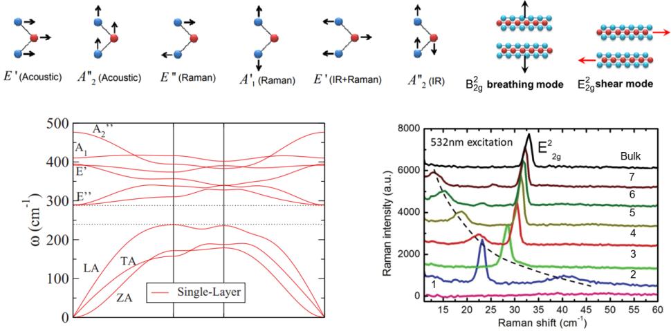
3.3. Opticalphonons Phononisthequantumofthevibrationsinacrystallattice.Thesevibrationsareuniquetothechemistryandthestructureofthematerial.Phonons andphonondispersionshavebeenwidelystudiedfor2Dmaterialswithfirstprinciplestheoreticalprediction59 andexperimentalobservations.60 Raman spectroscopyisapowerfulexperimentaltooltomeasureandprobethese phononsandcharacterizethese2Dmaterials.Inthissection,wewillfocus onphononsinamodelTMDwithfewlayers.
TMDscanberepresentedbyanX–M–Xstructure,withMbeinga transitionmetalsandwichedbetweentwoXchalcogenatomsarrangedin ahexagonallatticetermed2H.Theprimitiveunitcellforthisstructure hassixdifferentatomicpositions;hence,thereare18differentphonons (15opticaland3acoustic)attheΓpointintheBrillouinzone.61 Thesemodeshavebeenhighlightedforamonolayer2H-MoS2 filmin Fig.5(a).ThephonondispersionformonolayerMoS2 isshowninFig.5(b). Experimentally,E2g andA1g modesforMoS2 areobservedusing532nm laserexcitationandcanbeusedtodeterminethenumberoflayersinthe 2Dmaterialsbyprobingthedifferenceinthepeakpositionsofthesetwo peaks.62 Thelayer-dependentshiftoccursduetotheblueshiftingofthe A1g modeandredshiftingoftheE2g modeonincreasingthickness.Similar phonondispersioncalculationsandlayer-dependentRamanspectrahave alsobeenevaluatedforotherTMDs.61
Thephononsdiscussedabovecorrespondtovibrationsoccurringwithin asinglelayerof2Dmaterial.However,iftherearetwoormorelayersof 2Dmaterials,coupledvibrationsbetweenthoselayerscanoccur,leading tointerlayerphonons(Fig.5(c)).63 Theseinterlayerphononstypicallyhave verylowenergyasinterlayerbondingin2Dmaterialsisinherentlyweak andisobservedatlowwavenumbersinRamanspectra,asseeninFig.5(d). E2 2g istheinterlayershearmodewhoseenergyincreaseswithanincrease inlayernumber.ThedottedlineinFig.5(d)representslayerbreathing mode,whichcorrespondstothesimultaneousupanddownmovement
Figure5.OpticalphononmodesofMoS2 .(a)Thevibrationalmodesformonolayer MoS2 .AdaptedwithpermissionfromRef.60 c 2013AmericanChemicalSociety. (b)CalculatedphonondispersionformonolayerMoS2 .Adaptedwithpermissionfrom Ref.59 c 2011AmericanPhysicalSociety.(c)Interlayerphononmodesforbilayer MoS2 .AdaptedwithpermissionfromRef.60 c 2013AmericanChemicalSociety. (d)Layer-dependentlow-frequencyRamanspectraofMoS2 showingshearandlayer breathingmodes.AdaptedwithpermissionfromRef.63 c 2012AmericanPhysical Society.
oftheentirelayer.Itsenergydecreaseswithanincreaseinthelayer number.Hence,theselow-frequencymodesalsobecomeanessentialtool forcharacterizinglayernumbers.2Dmaterialheterostructuresalsoexhibit theseinterlayerphonons,includingboththeshearandlayerbreathing modeswhosepeakpositiondependsonthetypeof2Dmaterialandthe couplingstrengthbetweenthem.30 Thepositionsofinterlayerphononsare alsodependentontherelativeorientationofthestackedheterolayers.31
4.EmergingOpticalPhenomena Theuniqueopticalcharacteristicsof2Dmonolayersandfewlayers distinguishthemfromtheirbulkcounterparts.Inadditiontothestrong opticalabsorption,excitoniceffect,andphononbehaviors,2Dmaterials possessunconventionalopticalphenomenainducedbymoir´estacking.The excitonandphononpropertiescanbemodulatedbytheperiodicmoir´ e potential.Inadditiontothenarrowemissionlinesgeneratedbymoir´ e lattice,defectengineeringcanalsobeusedtogeneratesinglephotonsfrom thedefectstatesin2Dmaterials.Thestronglight–matterinteractionof