Nanomaterials in Clinical Therapeutics
Synthesis and Applications
Edited by Mainak Mukhopadhyay and Arindam Kuila
This edition first published 2022 by John Wiley & Sons, Inc., 111 River Street, Hoboken, NJ 07030, USA and Scrivener Publishing LLC, 100 Cummings Center, Suite 541J, Beverly, MA 01915, USA © 2022 Scrivener Publishing LLC
For more information about Scrivener publications please visit www.scrivenerpublishing.com.
All rights reserved. No part of this publication may be reproduced, stored in a retrieval system, or transmitted, in any form or by any means, electronic, mechanical, photocopying, recording, or otherwise, except as permitted by law. Advice on how to obtain permission to reuse material from this title is available at http://www.wiley.com/go/permissions.
Wiley Global Headquarters
111 River Street, Hoboken, NJ 07030, USA
For details of our global editorial offices, customer services, and more information about Wiley products visit us at www.wiley.com.
Limit of Liability/Disclaimer of Warranty
While the publisher and authors have used their best efforts in preparing this work, they make no representations or warranties with respect to the accuracy or completeness of the contents of this work and specifically disclaim all warranties, including without limitation any implied warranties of merchantability or fitness for a particular purpose. No warranty may be created or extended by sales representatives, written sales materials, or promotional statements for this work. The fact that an organization, website, or product is referred to in this work as a citation and/or potential source of further information does not mean that the publisher and authors endorse the information or services the organization, website, or product may provide or recommendations it may make. This work is sold with the understanding that the publisher is not engaged in rendering professional services. The advice and strategies contained herein may not be suitable for your situation. You should consult with a specialist where appropriate. Neither the publisher nor authors shall be liable for any loss of profit or any other commercial damages, including but not limited to special, incidental, consequential, or other damages. Further, readers should be aware that websites listed in this work may have changed or disappeared between when this work was written and when it is read.
Library of Congress Cataloging-in-Publication Data
ISBN 9781119857235
Cover image: Pixabay.Com
Cover design by Russell Richardson
Set in size of 11pt and Minion Pro by Manila Typesetting Company, Makati, Philippines Printed in the USA
10 9 8 7 6 5 4 3 2 1
Nabya Nehal, Anushka Mathur, Modhumita Ganguli and Priyanka Singh
4.1.1
4.1.2
Sharmili Roy, Monalisha Ghosh Dastidar, Vivek Sharma, Beom Soo Kim and Rajiv Chandra Rajak
5.1
5.3
5.5
6.3
Swarnalok
6.4
6.6.3
6.6.4
7.3
7.7
7.8
7.9
7.10
8.6
8.7
Bhattacharya
11 Instrumentation for the
Andrea Komesu, Johnatt Oliveira, Débora Kono Taketa Moreira, Yvan Jesus Olortiga Asencios, João Moreira Neto and Luiza Helena da Silva Martins
12
Monika Yadav, Sneha Upreti and Priyanka Singh
12.2.1.5
12.2.1.6
12.2.1.7
12.2.3.4
12.2.5.1
Part 3: Application of Nanomaterials
Kaliyaperumal Rekha, Nalok Dutta, Muthu Thiruvengadam, Mohammad Ali Shariati, Muhammad Usman Khan, Muhammad Usman, Mihir Bhatta, Kunal Ghosh, Shaheer Arif and Muhammad Naeem
15.1
15.2
15.3
15.5
Rituparna Saha and Mainak Mukhopadhyay
16.3
16.4
16.6
16.7
Preface
Nanotechnology-based applications is a rapidly growing field encompassing a diverse range of disciplines that impact our daily lives. Nanotechnology is being used to carry out large-scale reactions in practically every field of biotechnology and healthcare. The incredible progress being made in these applications is particularly true for the healthcare sector, where they are used in cancer detection and treatment, medical implants, tissue engineering, and so forth. Expansions in this discipline are expected to continue in the future, resulting in the creation of a variety of life-saving medical technology and treatment procedures.
The primary goal of this book is to disseminate information on nanotechnology’s applications in the biological sciences. A broad array of nanotechnological approaches utilized in different biological applications are highlighted in the book’s 17 chapters, including the employment of nanotechnology in drug delivery. The first three chapters provide an overview of the history and principles of nanotechnology. The synthesis, characterization, and applications of nanomaterials are covered in the next 10 chapters. The last four chapters discuss the use of nanomaterials in clinical research.
A number of well-known scientists contributed to the book, whose knowledge of the subject will benefit students and researchers in fields such as environmental biotechnology, bioprocess engineering, renewable energy, chemical engineering, nanotechnology, biotechnology, and microbiology.
We are grateful to Linda Mohr and Martin Scrivener at Scrivener Publishing for their complete cooperation and assistance in the timely publishing of this book. We would also like to express our gratitude to the writers and the publication staff for their efforts throughout the COVID19 epidemic.
Dr. Mainak Mukhopadhyay Dr. Arindam Kuila
June 2022
Introduction to Nanotechnology
Rekha Sharma1, Kritika S. Sharma2 and Dinesh Kumar2*
1Department of Chemistry, Banasthali Vidyapith, Rajasthan, India
2School of Chemical Sciences, Central University of Gujarat, Gandhinagar, India
Abstract
For the synthesis of material of nanometer size, nanotechnology implies an innovative route for technological development. Nanotechnology exactly means any technology in its various applications in the real world on the nanoscale. At scales ranging from discrete molecules or atoms to submicron dimensions, nanotechnology precisely includes the fabrication and application of chemical, physical, and biological systems, via the incorporation of these resulting nanomaterials into larger systems. It has the ability to alter our prospects, outlooks and proposals’ capability to overcome global problems. The introduction of many new areas of technology in nanocomposites, nanosensors, and nanomedicine has been done via the production and usage of nanomaterials. Currently, to produce the next generation of functional materials, nanotechnology is accomplished with its wide-ranging usage. Through attaining an important attention of the optical, magnetic, and mechanical properties of nanostructures, it is obtained as a multidisciplinary field. Furthermore, nanostructures can similarly give determinations toward technological and environmental challenges, and also in the areas of medicine, water treatment, catalysis, and solar energy conversion. This chapter mainly focusses on the classification of nanomaterials, introduction of nanotechnology, and the properties of nanomaterials.
Keywords: Nanotechnology, nanomaterials, biosensors, nanometer, nanostructures
*Corresponding author: dinesh.kumar@cug.ac.in
Mainak Mukhopadhyay and Arindam Kuila (eds.) Nanomaterials in Clinical Therapeutics: Synthesis and Applications, (3–32) © 2022 Scrivener Publishing LLC
1.1 Introduction
The scientific community is attracted by the nanoscience field. So nanotechnology is an outlook basically for most of the continuing deliberations, explanations, and considerations. Intrinsically, it establishes the apotheosis of human’s incessant need for knowledge and represents a broad term partaking applied potential. Nanotechnology is any technology to form functional structures by employing single atoms and molecules on the nanoscale, which has wide-ranging applications [1]. The area of nanotechnology comprises the utilization and creation of biological, physical, and chemical systems with structural features among single atoms or molecules to submicron dimensions, and also the assimilation of resultant nanostructures into larger systems [2, 3]. The technology on the nanoscale is simply called nanotechnology. Therefore, nanotechnology is the field, which comprise the materials in 1 to 100 nm range. The “engineering with atomic precision” and “atomically precise technology” are the brief definition of nanotechnology [4]. Owing to their nanoscale size, nanotechnology signify innovative, suggestively enhanced biological, physical, and chemical properties, developments, and methods. “The size and shape-controlled usage of matters to design, characterization, and manufacture in the nanoscale” is the dictionary description of the term nanotechnology [5]. Additionally, so as to make devices, systems, and matters through essentially innovative functions and properties, “the precision placement, controlled and careful manipulation, measurement, modeling, and production of materials at the nanoscale is a substitute definition [5]. In chemistry, colloidal science, biology, physics, and other scientific fields, nanotechnology is a branch of facts incorporating the study of methods at the nanoscale within a subclassification of technology [6]. The biological, physical, and chemical properties of materials at the nanoscale are demonstrated in the promise and essence of nanotechnology and nanoscience according to that they may be moderately diverse from those within a bulk material [7]. Dramatic changes can arise in their properties, when the dimensions are reduced below 100 nm of a material [7]. Therefore, to offer novel properties to a material along with variations associated precisely to structure and size, materials should be nanostructured so as to offer a precise performance. These types of particles and macromolecules possess distinct physicochemical properties at sizes of 1 to 50 nm and made of some molecules [8]. When nanoparticles (NPs) are used for similar applications, they possess properties of improved performance compared with bulk materials. The collection of atoms bonded in cooperation with an average size of 1 to
100 nm defines an NP, which characteristically comprising of 10 to 105 atoms [9]. Nanocatalysts are the important application of NPs which is the manufacture of a new class of catalysts [10]. For the enhanced performance of chemical reactions, significant developments are being made in the fields, which contribute to detailed understanding of manufacturing, function of NPs as catalysts and the nature of NPs, i.e., structure, composition, and particle size [11]. The purpose of the performance of catalysts is a commanding function of its size distribution and particle size. The chemical properties of NPs offer them with application as catalysts, which are linked to particle size, for example, electronic properties, surface morphology, and large surface-to-volume ratio [6, 12]. For the improvement of inventive nanosystems and nanostructured materials, innovative developments are done via the discovery of new processes, phenomena, and materials at the nanoscale. This is also done for the progression of innovative experimental and theoretical methods for research. In terms of its applications in electronics, agriculture, energy, medicine, various anticipated and recent improvements in nanotechnology and nanoscale science have been done at an increasing rate [10, 13]. In the extension of innovative methods used to substitute present production equipment, to create new products, and to reformulate chemicals toward improved performance and novel materials, nanotechnology can play an important part. It results in less energy consumption and reduced material, environmental remediation, and also for less toxicity to the environment [14]. Nanotechnology offers the thrilling opportunity by a more sustainable route to remediate problems, although a reduced ingesting of energy and matter, assists the environment. Environmental applications of nanotechnology comprise the measures to address both the resulting issues with the advancement of solutions to recent ecological problems, from the possible risks associated with nanotechnology, and interactions of energy and material with the atmosphere [14].
1.2 Nanoscale Materials: Importance
The definition of nanometer (nm) scale can be demonstrated as smaller than one tenth of a micrometer in at least one dimension or three to five atoms in width—equivalent to 10 A˚ or one billionth of a meter [15], although the materials smaller than 1 mm can be used as term nanoscale. Similarly, 1 nm is 10,000 times less than the diameter of a human hair or we can simply say 109 m. A method based on science has been derived in
the nanomaterial field, because of study materials at the nanoscale with structural features [15]. Nanotechnology and nanoscience functions have smaller systems and objects [16]. The systems and matter, which have the succeeding main properties, are defined as nanoscience studies:
➢ Building block property which permit the manufacture of larger structures,
➢ Apply methods that demonstrate the vital control of the chemical and physical appearances of molecular-scale structures.
➢Partake as a minimum of one dimension less than 10 nm.
Generally, developing the constituents of cellular structures to form the bioentities in the body, the nanotechnology is utilized in nature, for example, enzymes, proteins, DNA, carbohydrates, viruses, and RNA. Generally, the molecular size of various structures has 1 to 100 nm nanoscale range in biological system, nanoscience is actually characteristic of nature in the biological sciences [17]. For the development of advanced nanosystems and nanoscale matters, the study of innovative nanoscale phenomena, processes, and materials offers new prospects and also to the progress of novel experimental and theoretical methods. The nanoscale materials can be enormously dissimilar from larger scale materials on the dimensional scale. The nanostructures are categorized as the largest molecules and atoms in bulk materials or living systems or connecting the smallest part of artificial devices [18]. A drastic change can arise in their properties, when the material dimensions are condensed to less than 100 nm from a large size [19]. On the basis of morphology and distribution, ascendancy of size incarceration, quantum effects, and interfacial method, the utmost required properties at the nanoscale can be attained. Additionally, in terms of their different property at the macroscale, the materials behavior is not entirely predictable at the nanoscale [9, 20]. To demonstrate new biological, physical, and chemical properties of systems, the capability to operate and control nanostructures will finally make it possible. The properties are transitional in size, specifically, bulk materials, single atoms, and molecules [15]. Materials can be nanostructured in order to create novel properties and provide improved performance. The main reasons of nanoscale materials are comprised succeeding, which makes them very important for new opportunities in technology and science [16]:
➢ The enhanced surface area-to-volume ratio occurs in utmost nanoscale constituents, which offers likely novel quantum mechanical effects. Therefore, owing to this “quantum size
effect” with huge decrease in particle size, the electronic properties of solids can be altered [21]. For example, because of the close incarceration producing quantum effects by their electrons, NPs generally partake unexpected visual properties, for instance, in solution, the deep red to black color of gold NPs appears. To change the macroscopic and microscopic properties of NPs, a design of nanoscale materials used which comprise charge capacity deprived of changing their chemical composition, magnetization, and melting temperatures [16].
➢ Because of surface and interfacial chemistry, and large surface-to-volume ratios, chemical properties at this scale offer a use for catalysis, which is important for various uses. These nanoscale materials are perfect for composite materials, catalysis, energy storage, reacting systems, and drug delivery. Owing to various properties, they are being used in medicine field as well for instance possibility of being used to kill bacteria, and improved resistance property. Though there are concerns associated to the potential significances to the human health and environment [22], nanoscale materials partake the capacity to progress the environment by the manufacturing of customer products in terms of fabricating ecologically accountable products their designing and cleaner industrial procedures [22]. Applications, such as modifiable photoactive materials, materials of amplified strength, and creating catalysts, are offered by the innovative and inimitable properties of NPs, nanostructured materials, and other related nanotechnologies. Furthermore, in the area of medicine, catalysis, water treatment, and conversion of solar energy, such materials can be utilized to make solutions to face ecological and technical challenges [9, 23].
➢ The biological entities or molecular structures at the nanoscale is their systematic organization in the body, which allowed us to put artificial nanoscale stuffs into living cells [24]. Correspondingly, by the use of molecular self-assembly to examine the macrostructure and microstructure of matter, this technology has offered the possibility. In materials science, this surely is a precise commanding tool [25].
➢ The light-weight nanocomposites, enhanced hardness and strength of nanomaterials and developed malleability, and enhanced compression properties are the enriched
mechanical properties invented of nanostructures of macroscopic systems [26]. Moreover, in contrast to the microstructures, nanosystems may partake increased densities. Along with substantially condensed consumption of power concurrently through monitoring complexity and interactions of nanostructures, and being improved electricity conductors having faster and smaller circuits, and which can spark the manufacture of new electronic devices with more sophisticated functions [23].
1.3 Nanotechnology: Historical Advances
The famous Nobel Laureate and the physicist Dr. Richard P. Feynman introduced the concept of nanotechnology [27]. “There’s Plenty of Room at the Bottom: An Invitation to Enter a New Field of Physics” was the title of his classic science lectures. Feynman contemplated representing thin-film formation, miniaturization by evaporation, constructing small matters with atoms, for example by using nanorobotics solving the problems of lubrication, small factories, small machines, and electronic circuits. Similarly, to produce different nanodevices and nanostructures, he suggested the rearranging atoms [28]. In the field of medicine, AuNPs partake an extensive history. Such as, a patent for manufacturing stained glass incorporating gold NPs granted in 1449 by John Utynam who is a Flemish glassmaker in England. To patients suffering from certain illnesses, Hohenheim administered and synthesized gold NPs in the early 16th century. Several researchers working around the world in nanotechnology field on all the ideas presented in Feynman’s lecture [29–31]. The aligning of single atoms through a scanning tunneling microscope (STM), the manipulation of single atoms on a silicon surface, the trapping of 3D, single, colloidal particles using electrostatic techniques having nanometer-diameter are the successful applications resulted by the Feynman’s lecture in 1959. They nanomaterials have the possible to be working for uses in commercial enterprises, such as industry, because of the important effect of their enabling nature in these new systems. Because of their incapability to recognize the NPs structure, the efficiency of their research has been limited, though scientists have been working for decades with NPs. First of all, Tanaguchi used the term “nanotechnology,” in his paper presented in 1974 entitled “On the basic concept of nanotechnology” [32]. The potential of nanotechnology being promoted in the coming era of nanotechnology [33]. To manufacture complex nanomachines proteins could be used through customized
specifications in the drexler bottom-up approach. Such a nanodevice have specialized functions and would mimic biological processes in addition to undergoing self-destruction and self-replication as well. Nanotechnology is certainly in progress to advancement in the 1980s, after the development of the scanning electron microscope. Thus, the “Feynman scale” (’nman) was proposed [6]:
Feynman (φ) = 10-9 m = 10-3 μ = 10 Å
1.4 Nanofabrication Methods in Nanotechnology
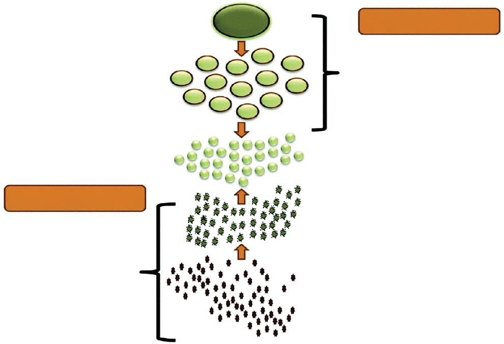
In nanotechnology, several methods have been utilized fruitfully. Novel methods will arise as the technology further progresses. Usually, through the background experiences of existing technology and researchers, the methods have been verbalized developed up to now. In numerous fields of science, for example chemistry and physics, nanotechnology has diverse definitions, and everyone recognizes its concept. With the aim to develop the next level of progression in nanotechnology, the multidisciplinary fields of nanotechnology, including chemistry, physics, electronics, biology, social sciences, and engineering, are all required to combine. By the use of nanotechnology, molecular electronics, fuel cells, nanobiological devices, mechanically strong materials, diamond molecules, quantum devices, graphene, and carbon nanotubes (CNTs) have been developed. The atomic-scale fabrication and top-down approach has been represented through “Rearranging the atoms” to develop diverse nanodevices and nanostructures, and bottom-up approach represented through the consideration of the “demeanor of atoms in a small world” [34, 35]. Through altering constituents of much larger devices via monolithic processing, the “topdown” method is based on the combination of structures. In semiconductor devices utilized in customer electronics, this method has been applied with outstanding accomplishment. Instead, through the systematic selfassembly of matter, atoms, or molecules, the “bottom-up” approach comprises the manufacture of device structures, which arrange molecules or atoms in nanostructures [36]. Nature is used to repair cells, tissues, and organ systems in living organisms by the use of “bottom-up” approach as shown in Figure 1.1, along with for life processes counting protein synthesis. The development of new concepts for tools and machines on a molecular level is of significant interest not only to mainstream research but also as a means to facilitate control of the characterization and synthesis of novel nanostructures, which yields a variety of novel products
One
Top Down Approach
Mechanical Milling
Etching
Laser Ablation
Sputtering
Electro-explosion
Nanoparticles
Supercritical Fluid Synthesis
Spinning
Sol-gel Process
Laser Pyrolysis
Chemical Vapour Deposition
Molecular Condensation
Chemical Reduction
Green Synthesis
Nuclei and its growth
Molecular/Atomic Level
Figure 1.1 Schematic representation of top-down and bottom-up approach [reprinted from the permission of Attribution-Non Commercial 3.0 Unported Licence reference 3. Copyright 2021 Royal Society of Chemistry].
of potential usage in the near future. Such procedures harvest ever tiny substances by working with such permitting, feasible researchers, which is the key developments via miniaturization. The development in advanced techniques is required with the purpose to do so [35]. Furthermore, corresponding to innovative applications, the incorporation of constantly minor matters, with constant increase in their numbers. Through the chemical processes of supramolecular constructs and self-assembling materials, the demonstration of self-organizing and organized objects has been done in the biological world.
1.4.1 Top-Down Method
The top-down method has been used by the reduction of constituents for the development of devices and machines with more efficiency. In the top-down method, the chemical, mechanical, or additional energy forms is used to convert a bulk material into its smaller pieces. At utilizing the top-down method, the electronics industry is the utmost fruitful manufacturing. At the micro/nanoscale, to manufacture functional structures,
Bulk Material
Bottom Up Approach
electronics industry uses approaches, which comprise a variety of methods, for example chemical vapor deposition (CVD), physical vapor deposition (PVD), X-ray lithography, photolithography (lithography), plasma and wet etching, and electron beam [37–39]. To manipulate increasingly tiny constituents of matter, this method has led physicists and engineers by photolithography techniques and others. The appearance of numerous instruments and electronic products have facilitated by research and development of these techniques, which has improved worldwide excellence of life. The progress of equipment linked with lithographic technology, as well as the advances in deposition technique, are equally significant and has been enhanced in the top-down approach. For instance, in terms of resolution, the ion-beam lithography methods, electron-beam lithography, and X-ray lithography have attained applications. Destructive effects on substrates and the cost are the drawbacks linked with these types of optics. Presently, with the purpose of advance recent lithographic processes, these approaches are examining which are used in the combined circuits industry. A novel production of stimulating products and features is being formed. These represents the conversion from microtechnology to nanotechnology because of incessant progresses in these techniques. The ion-beam lithography, photolithography, atom lasers, electron-beam lithography, through exponential enrichment (SELEX) the systematic evolution of ligands, LbL assembly, and coprecipitation are the methods to develop diverse NPs. Figure 1.1 shows the example of different methods on how they can be linked with each other to produce a special nanostructure [37]. Here, the used method was ion beam-chemical vapor deposition (FIB-CVD). The top-down method is being progressively interesting, for instance, the reduction of computer technology is rapidly reaching its maximum on silicon-based chips [37, 38]. Precisely, photolithography has vital economic and technical limits of less than 100 nm dimension, this is because of the large size contrast to atoms or molecules, but has extremely small size in terms of the standards of everyday life. Therefore, as Feynman presented in a famous talk, for significant reduction, there is abundance of room available at the bottom. Although providing this type of an opportunity, the top-down method does not seem accomplished.
1.4.2 Bottom-Up Method
The nanotechnology is implemented on the bottom-up approach, which is one of the most alternative and promising approaches at the nanoscale for science and technology. Top-down method is the opposite of this approach. To develop nanodevices and nanomaterials, the bottom-up
method signifies from basic chemical building blocks of the self-assembly of machines, molecules, and atoms. At the molecular level, this formation enables the progress of macroscopic concepts for devices and machines. In the development and growth of nanotechnology and nanoscience, this method fascinates the researcher’s interest. This method mainly comprises the areas of nanotechnology and nanoscience. In contrast to lithographical approaches, bottom-up method will correspond to the formation of inexpensive methods to make nanostructures of 2–10 nm of dimensions by the use of prudently controlled chemical reactions atom by atom. Generally, to develop complex structures, self-assembly is often utilized which are inadequate to moderately simple structures. For additional self-assembly steps, these self-assembly, which go on to form the base products, assists with the formation of complex or hierarchical systems. To develop multifaceted nanodevices with modified properties, the use of bottom-up approach of proteins demonstrated by drexler. Therefore, these type of nanodevices may be capable to precise applications, like selfdestruction and self-replication, which will mimic biological processes. The nanofabrication comprises some additional nanostructures, for example, frequently and naturally developed nanochannels of zeolites. For the formation of novel materials, i.e., porous carbon, these can be used in water treatment to check adsorbed water by the use of well-ordered zeolite channels or through bikitaite, which is a scarce lithium-containing zeolite. The carbon nanotube (CNT) is the most publicized material in recent years, and the molecular structures of these can be long chains of carbon or thin cylindrical tubes. The quantum dots and CNT crystals, which contain only a few hundred atoms, release diverse wavelengths of light upon excitation on the basis of their size, which can be developed using bottom-up method. Therefore, to tag nucleic acids and proteins, the developed quantum dots can be utilized. They can be utilized to discover attached proteins and when illuminated with ultraviolet light can also fluoresce. Lithography allows ink impressions to be kept. For nanofabrication and microfabrication, lithographic methods are massively significant. Newly, in the smaller features and characteristics, because of numerous confines of photolithographic processes, there are challenges to develop and improve new lithographic approaches having improved resolve. Certainly, an AFM scanning probe nanopatterning method used in the field is dip-pen nanolithography (DPN), which is recent development to distribute molecules to a surface in the ambient atmosphere using a solvent meniscus. Comprising monolayer, metals, and semiconductors functionalized surfaces, this is a simple method which gives highresolution patterning capabilities to a number of biomolecular and molecular