Two-Dimensional Materials for Nonlinear Optics: Fundamentals, Preparation Methods, and Applications
Qiang Wang
Visit to download the full and correct content document: https://ebookmass.com/product/two-dimensional-materials-for-nonlinear-optics-funda mentals-preparation-methods-and-applications-qiang-wang/

More products digital (pdf, epub, mobi) instant download maybe you interests ...

Two-Dimensional-Materials-Based Membranes: Preparation, Characterization, and Applications Gongping Liu
https://ebookmass.com/product/two-dimensional-materials-basedmembranes-preparation-characterization-and-applications-gongpingliu/

Defects in Two-Dimensional Materials Rafik Addou
https://ebookmass.com/product/defects-in-two-dimensionalmaterials-rafik-addou/


Computational Methods for Nonlinear Dynamical Systems: Theory and Applications in Aerospace Engineering Xuechuan Wang
https://ebookmass.com/product/computational-methods-fornonlinear-dynamical-systems-theory-and-applications-in-aerospaceengineering-xuechuan-wang/
Two-Dimensional (2D) NMR Methods Konstantin Ivanov
https://ebookmass.com/product/two-dimensional-2d-nmr-methodskonstantin-ivanov/


Nano-Optics: Fundamentals, Experimental Methods, and Applications (Micro and Nano Technologies) 1st Edition Sabu Thomas (Editor)
https://ebookmass.com/product/nano-optics-fundamentalsexperimental-methods-and-applications-micro-and-nanotechnologies-1st-edition-sabu-thomas-editor/
Nonlinear optics 4th ed Edition Boyd
https://ebookmass.com/product/nonlinear-optics-4th-ed-editionboyd/
Calculations and Simulations of Low-Dimensional Materials : Tailoring Properties for Applications 1st Edition Ying Dai
https://ebookmass.com/product/calculations-and-simulations-oflow-dimensional-materials-tailoring-properties-forapplications-1st-edition-ying-dai/
Tribology of Graphene: Simulation Methods, Preparation Methods, and Their Applications Oleksiy V. Penkov
https://ebookmass.com/product/tribology-of-graphene-simulationmethods-preparation-methods-and-their-applications-oleksiy-vpenkov/
Spintronic 2D Materials: Fundamentals and Applications (Materials Today)
Wenqing Liu (Editor)
https://ebookmass.com/product/spintronic-2d-materialsfundamentals-and-applications-materials-today-wenqing-liu-editor/

Two-DimensionalMaterialsforNonlinearOptics
Two-DimensionalMaterialsfor NonlinearOptics
Fundamentals,PreparationMethods,andApplications
EditedbyQiangWangandHao-LiZhang
Editors
Prof.QiangWang LanzhouUniversity CollegeofChemistryandChemical Engineering No.222TianshuiSouthRoad 730000Lanzhou China
Prof.Hao-LiZhang LanzhouUniversity CollegeofChemistryandChemical Engineering No.222TianshuiSouthRoad 730000Lanzhou China
CoverImages:©SergMyshkovsky/Getty Images;©Marco_de_Benedictis/ GettyImages
Allbookspublishedby WILEY-VCH arecarefully produced.Nevertheless,authors,editors,and publisherdonotwarranttheinformation containedinthesebooks,includingthisbook, tobefreeoferrors.Readersareadvisedtokeep inmindthatstatements,data,illustrations, proceduraldetailsorotheritemsmay inadvertentlybeinaccurate.
LibraryofCongressCardNo.: appliedfor
BritishLibraryCataloguing-in-PublicationData Acataloguerecordforthisbookisavailable fromtheBritishLibrary.
Bibliographicinformationpublishedby theDeutscheNationalbibliothek TheDeutsche Nationalbibliothekliststhispublicationinthe DeutscheNationalbibliografie;detailed bibliographicdataareavailableontheInternet at <http://dnb.d-nb.de>.
©2024WILEY-VCHGmbH,Boschstraße12, 69469Weinheim,Germany
Allrightsreserved(includingthoseof translationintootherlanguages).Nopartof thisbookmaybereproducedinanyform–by photoprinting,microfilm,oranyother means–nortransmittedortranslatedintoa machinelanguagewithoutwrittenpermission fromthepublishers.Registerednames, trademarks,etc.usedinthisbook,evenwhen notspecificallymarkedassuch,arenottobe consideredunprotectedbylaw.
PrintISBN: 978-3-527-35059-9
ePDFISBN: 978-3-527-83826-4
ePubISBN: 978-3-527-83827-1
oBookISBN: 978-3-527-83828-8
Typesetting Straive,Chennai,India
Contents
Preface xiii
ListofAbbreviations xv
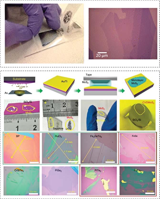
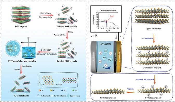
1Preparationof2DMaterials 1 YueTangandHuaXu
1.1MechanicalExfoliationof2DMaterials 2
1.2Liquid-PhaseExfoliationof2DMaterials 4
1.3ChemicalVaporDepositionGrowthof2DMaterials 6
1.4CVDGrowthofWafer-ScaleSingleCrystal2DMaterials 8
1.5ThicknessControlinCVDGrowthof2DMaterials 10
1.6PhaseControlinCVDGrowthof2DMaterials 12
1.7SummaryandProspect 14 References 15
2AnIntroductiontotheNonlinearOpticalPropertiesof 2DMaterials 21
BolongWangandHao-LiZhang
2.1Introduction 21
2.2NonlinearOpticsof2DMaterials 22
2.2.1SHG,THG,andHHGSetups 24
2.2.2Four-WaveMixing 26
2.2.3Z-ScanTechniques 27
2.2.4NonlinearOpticalImaging 29
2.2.5Pump–ProbeTechniques 32
2.3Applicationof2DNonlinearMaterials 35
2.3.1OpticalLimiting 35
2.3.2Q-SwitchedandMode-LockedLasers 38
2.3.3OpticalSwitchandModulation 40
2.3.4OtherNonlinearOpticalPhenomena 41
2.4Prospect 43
2.4.1PreciseFabricationandFunctionalizationof2DMaterials 43
2.4.2HighResolutionSpatiotemporalCharacterizingTechniques 44
2.4.3NewPhysicsof2DMaterials 44
2.4.4Ever-LastingExpansionofApplications 44 Acknowledgment 45 References 45
3ModulationandEnhancementofOpticalNonlinearityin 2DMaterials 55 XinglinWenandQihuaXiong
3.1Introduction 55
3.2NonlinearOpticsin2DMaterials 57
3.2.1BasicsofNonlinearOptics 57
3.2.2ParametricNonlinearOptics 58
3.2.3NonparametricNonlinearOptics 59
3.3NonlinearityModulationin2DMaterials 60
3.3.1StructuralEngineering 60
3.3.1.1LayerNumber 60
3.3.1.2TwistedAngle 62
3.3.1.3StackingOrder 64
3.3.1.4EdgeStates 65
3.3.2OpticalModulation 66
3.3.2.1ExcitonicEffectsEnhancedNonlinearity 66
3.3.2.2Valley-DependentNonlinearity 69
3.3.2.3OpticalCavity-EnhancedNonlinearity 71
3.3.2.4All-OpticalModulation 73
3.3.3ElectricalModulation 75
3.3.4MagneticModulation 78
3.3.5Perspectives 78
AuthorContributions 78 Notes 79 Acknowledgment 79 References 79
4CharacterizingtheNonlinearOpticalPropertiesof 2DMaterialsbyDouble4fNonlinearImagingSystemwith PhaseObjectandFour-Wave-MixingMicroscopy 87 ZhongguoLiandYinglinSong
4.1Introduction 87
4.2PrincipleofNLOMeasurementTechnique 88
4.2.1NonlinearOpticalInteractionin2DMaterials 88
4.2.2TypicalNLOMeasurementMethodin2DMaterialResearch 89
4.2.2.1Self-PhaseModulation(SPM) 89
4.2.2.2Z-Scan 89
4.2.2.3Third-HarmonicGeneration(THG) 90
4.2.2.4Two-Photon-InducedPhotoluminescence(TPL) 90
4.3CharacterizingNLOResponseof2DMaterialsviaDouble4fNonlinear ImagingSystemwithPhaseObject(NIT-PO)Microscopy 91
4.4CharacterizingNLOResponseof2DMaterialsviaFour-Wave-Mixing Microscopy 95
4.5OutlookandPerspective 97 References 98
5UltrafastCarrierDynamicsinEmerging2DMaterials 103 JiaweiHuang,NingningDong,andJunWang
5.1Introduction 103
5.2UltrafastTime-ResolvedSpectroscopy 104
5.2.1PrincipleofPump–ProbeMeasurement 104
5.2.2ExperimentforUltrafastSpectroscopy 107
5.2.3FundamentalMechanismofRecombinationDynamics 107
5.3UltrafastOpticsinvanderWaals2DMaterials 109
5.3.1Graphene 109
5.3.2TransitionMetalDichalcogenides(TMDC) 109
5.3.3BlackPhosphorus 115
5.4UltrafastOpticsinEmergingQuasi-2DMaterials 118
5.4.12DPerovskite 118
5.4.2Non-Layered2DPlatinumSulfide 120
5.5PerspectivesonUltrafastOpticsfor2DMaterial 124 AuthorContributions 125 Notes 125
Acknowledgment 125 References 125
6TransientTerahertzSpectroscopyfor2DMaterials 131 JingyinXu,KaiZhang,HongLi,andTianwuWang
6.1Introduction 131
6.2GenerationandDetectionofTHzRadiation 132
6.2.1GenerationofTHzRadiationBasedonNonlinearOpticalProcesses 132
6.2.1.1PhotoconductiveAntennas(PCAs) 133
6.2.1.2Electro-optic(EO)Crystals 135
6.2.1.3AirPlasma 136
6.2.1.4THzEmissionof2DSemiconductorMaterials 140
6.2.2TypicalTHzTime-DomainSpectroscopySetup 141
6.2.2.1Time-DomainTHzSpectroscopyUnderPressure 143
6.2.3PhotoinducedChangesoftheDielectricFunctionin2DviaTHz Spectroscopy 147
6.3NanoscaleTHzScanningProbeMicroscopyof2DMaterials 149
6.3.1ScanningNear-FieldTHzMicroscopyforPolaritonin2DMaterials 150
6.3.2THz-STM 151
6.4Perspectives 154
6.4.1TransientTHzSpectroscopy 154
6.4.2High-ResolutionSpatialandTemporalTHzSpectroscopies 155
Acknowledgment 155 References 155
7GrapheneGlassforNonlinearOptics 163 QiXiao,JingyuSun,andHao-LiZhang
7.1LightAbsorptionofGraphene 163
7.2NonlinearOpticalPropertiesofGraphene 164
7.2.1Third-OrderNonlinearOpticalPropertiesofGraphene 164
7.2.2SaturableAbsorptionofGraphene 165
7.2.3High-OrderHarmonicGenerationofGraphene 165
7.3NonlinearOpticalPropertiesofGrapheneGlass 167
7.3.1Graphene-DopedGlass 167
7.3.2GrapheneGlassFabricatedbySpinCoating 167
7.3.3GrapheneGlassFabricatedbyTransferMethod 168
7.3.4DirectlyGrowthGrapheneonGlass 168
7.3.4.1GrapheneGrowthonHigh-Temperature-ResistantGlass 168
7.3.4.2GrapheneGrowthonMoltenGlass 171
7.3.4.3Metal-Catalyst-AssistedGrapheneGrowth 173
7.3.4.4Plasma-EnhancedLow-TemperatureGrapheneGrowth 176
7.4Perspectives 179
Acknowledgment 180 References 180
82DMaterialsforNonlinearOpticalLimiting 185 WenShang,BolongWang,andQiangWang
8.1Introduction 185
8.2NonlinearOpticalLimitingMechanism 186
8.2.1ReverseSaturableAbsorption 186
8.2.2Two-Photon/MultiphotonAbsorption 187
8.2.3FreeCarrierAbsorption 188
8.2.4NonlinearRefraction 188
8.2.5NonlinearScattering 189
8.32DMaterialsforOpticalLimiting 189
8.3.1GrapheneandAnalogs 190
8.3.1.1Graphene 190
8.3.1.2TransitionMetalDichalcogenides 194
8.3.1.3BlackPhosphorus 196
8.3.1.4HexagonalBoronNitride(h-BNS) 197
8.3.2Novel2DMaterials 197
8.3.2.1Antimonene 197
8.3.2.2Tellurene 198
8.3.2.32DPerovskites 200
8.3.2.42DMetal–OrganicFrameworks(2D-MOFs) 201
8.3.3MaterialswithNewStructuresandMechanism 203
8.3.3.1NonlinearPhotonicMetamaterials 203
8.3.3.2PlasmonicEffect-EnhancedNonlinearity 205
8.3.4MultifunctionalOpticalLimitingDevices 206
8.4ConclusionsandProspects 209 Acknowledgments 210 References 210
9TheSaturableAbsorbersBasedon2DMaterials 221 Xin-HaiYan,LeiZhang,andKai-GeZhou
9.1Introduction 221
9.2TheFundamentsinthe2DMaterials-BasedSaturableAbsorbers 222
9.2.1SATheory 222
9.2.2Slow-andFast-SaturableAbsorber 223
9.2.2.1Slow-SaturableAbsorber 224
9.2.2.2Fast-SaturableAbsorber 225
9.3TheFamilyof2DMaterial-BasedSaturableAbsorbers 225
9.3.1Mono-Elemental2DMaterials 226
9.3.1.1GroupIVA-Elemental2DMaterials 226
9.3.1.2GroupVA-Elemental2DMaterials 230
9.3.2Dual-Elemental2DMaterials 234
9.3.2.1TMDs 234
9.3.2.2TopologicalInsulators(TIs) 235
9.3.3Multi-Elemental2DMaterials 237
9.3.3.1MOFs 237
9.3.3.2MXenes 237
9.3.3.32DPerovskites 239
9.4Applications 239
9.4.1FabricationofSADeviceBasedon2DMaterials 239
9.4.1.1ScotchTapeExfoliation 240
9.4.1.2CVD,PVD 240
9.4.1.3LPE 240
9.4.2Q-SwitchedLaser 242
9.4.2.1Q-SwitchedFiberLaser 243
9.4.3Mode-LockedLaser 246
9.5PerspectivesandOutlook 248
Acknowledgment 249 References 249
10Second-HarmonicandThird-HarmonicGenerationsin 2DLayeredMaterials 257 XudongJinandMinZhao
10.1Introduction 257
10.1.1FundamentalsofSHGandTHG 258
10.1.22DLM-BasedSHG 259
10.1.3Graphene 260
x Contents
10.1.4TransitionMetalDichalcogenides 262
10.1.5Other2DLMs 266
10.1.62DLM-BasedTHG 268
10.1.6.1Graphene 268
10.1.7TransitionMetalDichalcogenides 268
10.1.7.1Other2DLMs 270
10.2ConclusionsandOutlook 274 References 274
112DPerovskitesforNanolasers 281
WeiYuanandChuanjiangQin
11.1Introduction 281
11.2LaserFormationPrincipleandPerformanceParameters 283
11.2.1BasicOpticalPhysicalProcess 283
11.2.2LaserFormationCondition 283
11.2.3PerformanceParameters 284
11.2.4OpticalCavities 285
11.3TheApplicationof2DPerovskitesinNanolasers 286
11.3.1Microplates 287
11.3.2Microrods 287
11.3.3Microcrystals 291
11.3.4Nanowires 291
11.3.5Microrings 293
11.3.6ThinFilms 294
11.3.7ThinFlakes 298
11.4Prospect 299 References 300
122DMaterialsforSpaceUse 303
ShuyanWangandQiangWang
12.1Introduction 303
12.2SpaceRadiationandTwo-DimensionalMaterials 305
12.2.1SpaceRadiationEnvironment 305
12.2.22DMaterialsUnderIrradiation 307
12.2.2.1ElectronIrradiation 307
12.2.2.2IonIrradiation 307
12.2.2.3ProtonIrradiation 308
12.2.2.4 γ-RayIrradiation 308
12.32DMaterialsforSpaceUse 309
12.3.1EmergingNonlinearOpticalApplications 309
12.3.1.1LaserProtectionandModeLocking 310
12.3.1.2OtherNonlinearPhenomena 313
12.3.2SpaceX-rayDetectionandImaging 314
12.3.3PerovskiteSolarCells(PSCs) 316
12.3.42DSingle-PhotonSources 317
12.3.5IntegratedOptoelectronicPlatform 318
12.3.5.1Field-EffectTransistorandPhotodetectors 318
12.3.5.2Sensors 320
12.3.6OtherApplications:Lubricants 320
12.4Perspectives 321
Acknowledgment 322
References 322 Index 333
Preface
Thedevelopmentoftwo-dimensional(2D)materialshasgarneredincreasing interestduetotheiruniquestructureandversatileapplications.Forinstance,inthe optoelectronicandphotonicfields,2Dmaterialshavebeenbroadlyemployedfor opticalmodulationthroughopticallimiting/modelocking,photodetectors,optical communications,miniaturizedall-opticaldevices,andsoon.Theever-expanding 2Dfamilyparticularlyoffersabundantsourcestotheemergingnewphysical insightsandphenomenaintraditionalnonlinearoptics.Althoughpreviously therehavebeenmanyexcellentreviewsontheapplicationsof2Dmaterialsinone specificfield,systematicintroductionintegratingallofthekeyelementsranging frommaterialfabricationstonovelcharacterizingtechniquesandmyriadnonlinear opticalapplicationsisstillrare.
Hence,inthisbook,collectiveeffortsthroughresearchersfrominterdisciplinary fieldsfocuson2Dmaterialsfornonlinearopticalapplicationstofurthertheexciting territorytowardanewhorizon.Preparationmethodsforvarious2Dmaterials includinggrapheneglass,transitionmetaldichalcogenides(TMDs),singleelemental2DmaterialsfromGroup15,andperovskiteshavebeenthoroughlysummarized. Moreover,powerfulnonlinearopticalcharacterizingtechniques,suchasZ-scan measurement,femtosecondtransientabsorptionspectroscopyandmicroscopyare introduced.Theoriginoftheuniqueoptoelectronicpropertiesof2Dmaterialsis elucidatedfromvariousperspectiveslikeexcited-statedynamics.
Specifically,Chapter1providesacomprehensiveperspectiveonthefundamentals andpreparationmethodsof2Dmaterialswithnonlinearopticalproperties.Chapter 2isanoverallintroductiontothenonlinearopticalpropertiesof2Dmaterials, andChapter3elaboratesonthemodulationandenhancementofopticalnonlinearityin2Dmaterials.Furthermore,Chapters4–6discussthenonlinearoptical characterizationtechniquesfor2Dmaterialsandtheirapplicationsinthespecific field,includingnovelnonlinearopticalimagingsystems,ultrafasttime-resolved spectroscopyforinvestigatingcarrierdynamicsinemerging2Dmaterials,transient terahertzspectroscopy,etc.Chapter7expoundsongrapheneglassfornonlinear opticswhileChapters8–12emphasizetheapplicationsof2Dmaterialsforoptical limiting,saturableabsorber,SHGandTHG,nanolasers,andspaceuse,respectively. Thetopicscoveredinthisbookareofvitalimportanceinunderstandingthe uniqueoptoelectronicpropertiesandapplicationsof2Dmaterialsandthephysical
xiv Preface
insightsbehindthem.Wehopethebookwillbeahandytoolkitforprofessionals, researchers,andgraduatestudentsworkingorinterestedinthefieldofnonlinear opticsandmaterials.
Theeditorsthankallthecontributorsofthisbookfortheirinsightfulchapters.We aregratefultotheproductioneditorsatWiley,Ms.LifenYangandKatherineWong, fortheirdiligentworkandexpertiseinmanagingtheprocess.
Lanzhou,People’sRepublicofChina QiangWang Hao-LiZhang
ListofAbbreviations
Number
2DTwodimensional
2DLMs2Dlayeredmaterials
2DCSTwo-dimensionalcoherentspectroscopy
1DOnedimensional
0DZerodimensional
2PATwo-photonabsorption
3PAThree-photonabsorption
3PMThree-photonmicroscopy
A
ABCDAir-biasedcoherentdetection
AC-STEMAberration-correctedscanningtransmissionelectionmicroscopy
AIEAggregation-inducedemission
AFMAtomicforcemicroscope
ASEAmplifiedspontaneousemission
B
BiBismuthene
BCBirefringencecrystals
BPBlackphosphorus
BSBeamsplitter
BPDsBalancedphotodiodes
BBOBetabariumborate
BNBoronnitride
BLGBilayergraphene
BGRBandgaprenormalization
xvi ListofAbbreviations
C
CARSAnti-StokesRamanscattering
CMOSComplementarymetal-oxidesemiconductor
CVDChemicalvapordeposition
CSSChineseSpaceStation
COFsCovalentorganicframeworks
CBConductionbands
CWContinuouswave
D
DACDiamondanvilcell
DFGDifference-frequencygeneration
DLCDiamond-likecarbon
D-ADonor–acceptor
DBRDistributedBraggreflector
DSMDiracsemimetal
DFWMDegenerateFWM
DTDifferentialtransmission
DFBDistributedfeedback
DWPDouble-wavelengthwaveplate
E
ESAExcited-stateabsorption
EDFErbium-dopedfiber
EBLElectronbeamlithography
ENZEpsilonnearzero
EDElectricdipole
EQElectricquadrupole
EOElectro-optic
EFISHElectric-field-inducedsecondharmonics
F
FWMFour-wavemixing
FWRFour-waverectification
fsFemtosecond
FCAFreecarrierabsorption
FETField-effecttransistor
FTOFluorine-dopedtinoxide
FWFundamentwavelength
F-PFabry–Pérotcavity
FWHMFullwidthathalfmaxima
G
GeGermanium
GOGrapheneoxide
GDGraphdiyne
GEOsGeostationaryorbits
GSAMGraphenesaturableabsorbermirror
H
HGHarmonicgeneration
HHGHigh-harmonicgeneration
h-BNHexagonalboronnitride
HEOsHighlyellipticalorbits
HAADFHigh-angleannulardarkfield
HTHightemperature
HPHalf-waveplate
HEGHydrogen-inducedexfoliatedgraphene h-MOHexagonalmetaloxides
I
ISSInternationalSpaceStation
IPAIsopropylammonium
L
LEEDLow-energyelectrondiffraction
LDLaserdiode
LEOsLow-Earthorbits
LiDARLightdetectionandranging
LDOSLocaldensityofstates
LPELiquid-phaseexfoliation
LAPCAsLarge-aperturephotoconductiveantennas
ListofAbbreviations xvii
xviii ListofAbbreviations
M
MMagnetization
MPLMultiphotonlithography
MPEAChiral β-methylphenethylammonium
MPAMultiphotonabsorption
MRRsMicro-ringresonators
MZIMach–Zehnderinterferometer
MEOsMedium-Earthorbits
MOFsMetal–organicframeworks
MOCVDMetal–organicchemicalvapordeposition
MRAMetamaterialresonantabsorber
MDMagneticdipole
MIMultiphotonionization
MSHGMagnetization-inducedSHG
MAEFMultiphoton-absorption-excitedfluorescence
MXenesTransitionmetalcarbidesandnitrides
N
NLONonlinearoptics
NLANonlinearabsorption
NLRNonlinearrefraction
NLSNonlinearscattering
NWsNanowires
NRsNanorods
NDsNanodots
NSsNanosheets
NIT-PONonlinearimagingsystemwithphaseobject
NMPN-methylpyrrolidone
O
OPAOpticalparametricamplifier
OMOpticalmicroscope
OLOpticallimiting
OCOutputcoupler
OAOpenaperture
OROpticalrectification
P
PMMAPolymethylmethacrylate
PDMSPolydimethylsiloxane
PEEMPhotoemissionelectronmicroscopy
PtPlatinum
PCPolarizationcontroller
PDPhotodiode
PCAsPhotoconductiveantennas
POPhaseobject
PI-ISOPolarization-independentisolator
PSEPolymersolidelectrolyte
PVDPhysicalvapordeposition
PVTPhysicalvaportransport
PBPhotoinducedbleaching
PMParabolicmirrors
PMTPhotomultipliertube
PIAPhotoinducedabsorption
PtSPlatinumsulfide
PMTPhotomultipliertube
Q
QWsQuantumwells
QDsQuantumdots
R
RSAReversesaturableabsorption
rGOReducedgrapheneoxide
RIEReactiveionetching
S
SHGSecond-harmonicgeneration
SRSStimulatedRamanscattering
SASaturableabsorption
SAESonication-assistedexfoliation
SEEsSingle-eventeffects
SEUSingle-eventupset
SEFISingle-eventfunctionalinterruption
SETSingle-eventtransient
SELSingle-eventlatch-up
SNSPDSuperconductingnanowiresingle-photondetectors
SDIspectral-domaininterferometry
SOISilicononinsulator
SEMScanningelectronmicroscopy
SFMSum-frequencymixing
ListofAbbreviations xix
xx ListofAbbreviations
SPMSelf-phasemodulation
SNOMScanningnear-fieldopticalmicroscopy
STESelf-trappedexciton
SVEASlowlyvaryingenvelopeapproximation
SESAMSemiconductorsaturableabsorbermirror
STMScanningtunnelingmicroscopy
STSScanningtunnelingspectroscopy
SECTSlowevaporationatconstanttemperature
SNRSignal-to-noiseratio
TTPATwo-photonabsorption
THGThird-harmonicgeneration
TPFTwo-photonfluorescence
TPFTiltedpulsefront
THzTerahertz
TFISHTHz-field-inducedsecondharmonic
TPLTwo-photonluminescence
TPEFTwo-photonexcitationfluorescence
TAMTransientabsorptionmicroscopy
TASTransientabsorptionspectroscopy
TACThermallyassistedconversion
TCRTransition-Cherenkovradiation
TMDsTransitionmetalchalcogenides
TMDCsTransitionmetaldichalcogenides
TITunnelionization
TIDTotalionizingdose
tr-SNOMTime-resolvedscanningnear-fieldopticalmicroscope
TRTSTime-resolvedTHztime-domainspectroscopy V
vdWvanderWaals
VBValencebands
ListofAbbreviations xxi
WTungsten
WPWollastonprism
WDMWavelengthdivisionmultiplexer
WGMWhispering-gallerymode
XUVExtremeultraviolet