1 | 2023 A PAN EUROPEAN MAGAZINE https://international.electronica-azi.ro INTERNATIONAL


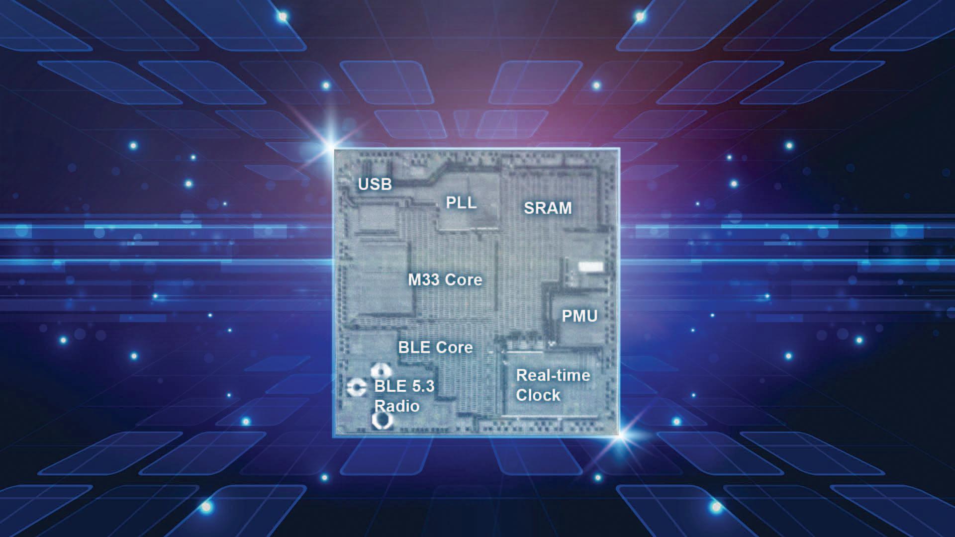
Wireless Microcontroller Integrating Bluetooth® 5.3 Low Energy Employs Most Advanced Process Node Available for MCUs

Renesas Electronics Corporation announced that it has produced its first microcontroller (MCU) based on advanced 22-nm process technology. By employing stateof-the-art process technology, Renesas can provide customers with superior performance at lower power consumption driven by reduced core voltages. The advanced process technology also offers the ability to integrate a rich feature set including functions such as RF. Additionally, the advanced process node uses a smaller die area for the same functionality, resulting in smaller chips with higher integration of peripherals and memory.
The first chip produced on the new 22-nm process is an extension to Renesas’ popular RA family of 32-bit Arm® Cortex®-M microcontrollers. This new wireless MCU delivers Bluetooth® 5.3 Low Energy (LE) with the integration of a software-defined radio (SDR). It offers a future-proof solution for customers building products targeting a long lifetime. Whether during development or after deployment, the devices can be upgraded either with new application software or new Bluetooth
capabilities to assure compliance to the latest specification versions. End product manufacturers can leverage the full feature set of previous Bluetooth LE specification releases. Whether designing devices for direction-finding applications utilizing the Bluetooth 5.1 Angle of Arrival (AoA) / Angle of Departure (AoD) features, or adding low power stereo audio transmission to products by employing Bluetooth 5.2 isochronous channels, developers now only need one device to support all of these features.
Renesas will combine the new 22-nm MCUs with numerous compatible devices from its portfolio to offer a wide array of Winning Combinations. These Winning Combinations are technically vetted system architectures from mutually compatible devices that work together seamlessly to bring an optimized, low-risk design for faster time to market. Renesas offers more than 300 Winning Combinations with a wide range of products from the Renesas portfolio to enable customers to
speed up the design process and bring their products to market more quickly. They can be found at renesas.com/win.
Renesas MCU Leadership

Renesas is the industry’s #1 supplier of MCUs, shipping more than 3.5 billion units per year, with approximately 50% of shipments serving the automotive industry, and the remainder supporting industrial and Internet of Things applications as well as data center and communications infrastructure. Renesas has the broadest portfolio of 8-, 16- and 32-bit devices, delivering unmatched quality and efficiency with exceptional performance. As a trusted supplier, Renesas has decades of experience designing smart, secure MCUs, backed by a dual-source production model, the industry’s most advanced MCU process technology and a vast network of more than 200 ecosystem partners. For more information about Renesas MCUs, visit renesas.com/MCUs.
Renesas Electronics Corporation


www.renesas.com

3 | Renesas Samples Its First 22-nm Microcontroller

6 | Nexperia releases leading-edge 650V Silicon Carbide diodes for demanding power conversion applications
7 | Infineon drives decarbonization and digitalization for a greener future with innovative semiconductor solutions at PCIM Europe 2023
8 | 50 years of interdisciplinary expertise for best-fit solutions
36 | How integrated features can save the day in your temperature measurement system
39 | Würth Elektronik offers WR-CIRCM12 M12-A circular connectors
39 | Contributing to a sustainable future: Toshiba proves its power credentials at PCIM 2023
40 | Flexible workflow for more efficient development
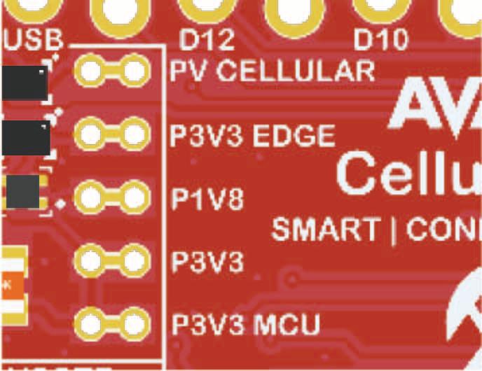
45 | Renesas Cellular-to-Cloud Development Kits Now Connect Seamlessly to Microsoft Azure Cloud Services
46 | Mouser Electronics Sponsors Nordic Semiconductor Connect for Good Challenge on Building a Smarter, More Sustainable Future
9 | MicroSys Electronics introduces evaluation kit for NXP S32G -based System-on-Modules
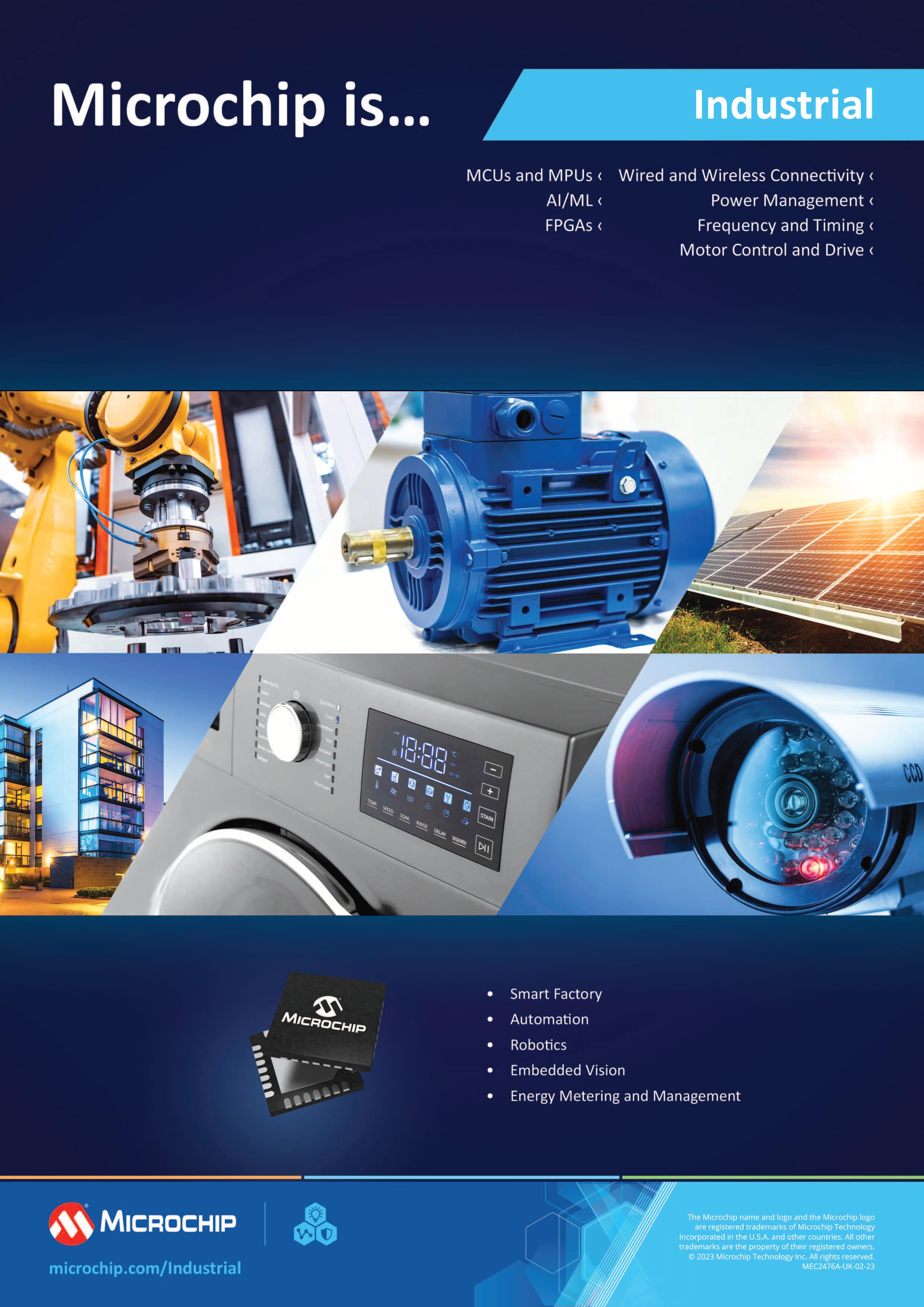
10 | Enabling Smart & Flexible Manufacturing with more Advanced Robotics
14 | Challenges in the design of radar transceivers for ADAS/AD

47 | u-blox and Position Partners roll out PointPerfect GNSS augmentation service to Australia
48 | SEGGER announces support for ST’s STM32C0 MCU series
48 | Navitas Power Forward with Next-Gen GaN and SiC Power Semiconductors at PCIM 2023
49 | Hi-Lo Systems supports Infineon’s OPTIGA™ TPM firmware programming to accelerate device manufacturers’ time-to-market

50 | New Dual Status Profiled Backlights™ combine two colours in a single device for cost-effective, dual-colour status indication in displays
50 | element14 Community launches ‘Path to Programmable III’
51 | New eBook from Apex Microtechnology and Mouser Offers Expert Perspectives on High Reliability Designs
18 | Why and How to Kickstart Cellular IoT Projects using Microchip’s IoT development board

24 | Product Procurement Expands with Digi-Key’s New myLists’ Features

27 | Wi-Fi 6 and Wi-Fi 6E the latest Wi-Fi standards
30 | How to Realize Power-Saving Analog-to-Digital Conversion for Highly Accurate Measurements

32 | DNA, PCR & Power Supplies - What do they have in common?
Management
Managing Director - I onela G anea
Editorial Director - Gabriel N eagu
Accounting - I oana P araschiv
Advertisement - Irina G anea
Web design - Eugen Vărzaru
Contributing editors

Cornel Pazara
PhD. Paul S vasta
PhD. N orocel C odreanu
PhD. Marian Blejan
PhD. B ogdan G rămescu
52 | Energy harvesting PMIC from Nexperia enables environmentally friendly energy-autonomous low-power devices
52 | Mouser Electronics Expands Smart Agriculture Content Hub with Resources for Engineers

53 | IAR Embedded Secure IP upgrades solutions portfolio with late-stage security
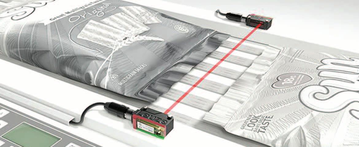
56 | Sensors with convincing cost effectiveness on conveyor lines and in the packaging industry
“Electronica Azi” is a registered trademark at OSIM - Romania, Registered position: 124259
ISSN: 1582-3490

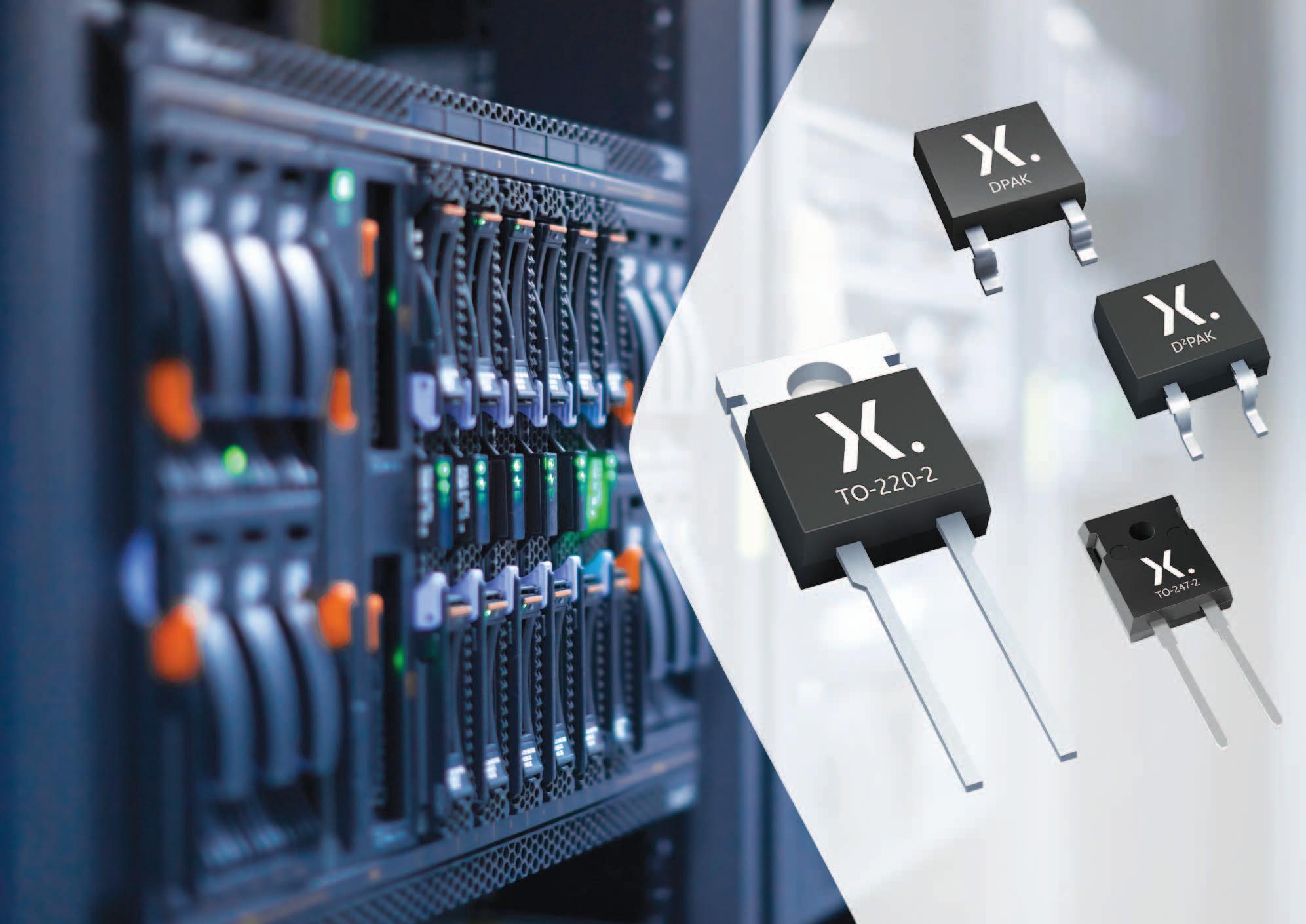
Nexperia, the expert in essential semiconductors, today introduced a 650 V Silicon Carbide (SiC) Schottky diode designed for power applications which require ultra-high performance, low loss, and high efficiency. The 10 A, 650 V SiC Schottky diode is an industrial-grade part that addresses the challenges of demanding high voltage and high current applications. These include switched-mode power supplies, AC-DC and DC-DC converters, battery-charging infrastructure, uninterruptible power supplies and photovoltaic inverters and allow for more sustainable operations. Data centers, for example, equipped with power supplies designed using Nexperia’s PSC1065K SiC Schottky diode will be better placed to meet rigorous energy efficiency standards than those using solely silicon-based solutions.
The PSC1065K delivers leading-edge performance with temperature-independent capacitive switching and zero recovery behavior culminating in an outstanding
figure-of-merit (QC x VF). Its excellent switching performance is almost entirely independent of current and switching speed variations. The merged PiN Schottky (MPS) structure of the PSC1065K provides additional benefits, such as outstanding robustness against surge currents that eliminates the need for additional protection circuitry. These features significantly reduce system complexity and enable hardware designers to achieve higher efficiency with smaller form factors in rugged high-power applications. Designers can be further reassured by Nexperia’s proven reputation as a supplier of high-quality products in a range of semiconductor technologies. This SiC Schottky diode is encapsulated in a Real-2-Pin (R2P) TO-220-2 throughhole power plastic package. Additional package options include the surface mount (DPAK R2P and D2PAK R2P) and through-hole (TO-247-2) with a real 2-pin configuration that enhances reliability in high-voltage applications at temperatures up to 175 °C.
Nexperia plans to continuously augment its portfolio of SiC diodes by including automotive-grade parts that operate at 650 V and 1200 V voltages with currents in the 6-20 A range. Samples and production quantities of the new SiC diodes are available now.
To learn more about Nexperia’s new 650 V SiC Schottky diodes, visit: www.nexperia.com/sic_diodes
You can also dive deeper with our blog posts “Why all SiC Schottky diodes are not made equal” and “8 Reasons Why Silicon Carbide Diodes Outperform their Silicon Peers”.
For a comparison of Nexperia’s PSC1065K with existing top-tier MPS and JBS counterparts see these charts:
• Switching behavior
• Efficiency in Power Factor Correction (PFC) topology
• Outstanding figure-of-merit Nexperia

Infineon Technologies AG (offers power solutions such as CoolSiC™ and CoolGaN™ that enable higher energy efficiency. This makes them key to sustainable designs and an important building block for the energy transition. At PCIM Europe 2023, Infineon will showcase how its latest solutions in power semiconductors and wide bandgap technologies provide answers to the current challenges of green and digital transformation. Under the motto “Driving decarbonization and digitalization. Together.”, the company will offer numerous demonstrations, live TechTalks, and the opportunity to discuss design challenges with experts. Alternatively, industry professionals can register for the Infineon’s virtual platform, which will be available around the clock from 27 April onwards.
WBG technologies take energy efficiency to the next level
Infineon’s wide bandgap (WBG) portfolio offers comprehensive options with excellent efficiency and very high power density. Highlights of Infineon’s wide bandgap portfolio include CoolGaN based USB-C adapters and chargers, as well as solutions
for e-mobility with CoolGaN SG HEMTs, EiceDRIVER™ gate driver ICs and XENSIV™ sensors. New chip technologies including HybridPACK™ Drive CoolSiC G2 simplify automotive electrification, and packaging innovations for Si, SiC and GaN power technologies with topside cooling (TSC) enable pushing the limits of efficiency and power density in high-performance industrial and automotive applications. These and other demonstrations will be showcased at Infineon’s booth #412 in hall 7.
• Energy transition technologies
• Electric vehicle charging solutions
• Energy efficient industrial automation
• Smart Home & Smart Building
• AI-powered analysis of machines and industrial equipment
In addition to the wide range of demonstrations, Infineon has organized a comprehensive series of TechTalks at its booth. The nine talks cover a wide range of topics including solid-state circuit breakers, energy storage systems, EV charging, heat pumps, hydrogen production, solar
and traction inverters as well as CoolSiC and CoolGaN solutions. In addition, Infineon experts will participate in the PCIM conference and poster sessions. Full details of Infineon’s conference presentations, technical workshops and TechTalks can be found here.
At the PCIM Europe 2023 tradeshow, Infineon is showcasing innovative product-to-system solutions for applications that will power the world and shape the future. Company representatives will also be giving several presentations at the accompanying PCIM Conference and Industry & E-Mobility Forum with live and on-demand video presentations, followed by discussions with the speakers. “Driving decarbonization and digitalization. Together.” at the Infineon booth #412 in hall 7, 9-11 May, 2023 in Nuremberg/Germany. Information about the PCIM Europe 2023 show highlights is available at www.infineon.com/pcim
Infineon Technologies
www.infineon.com
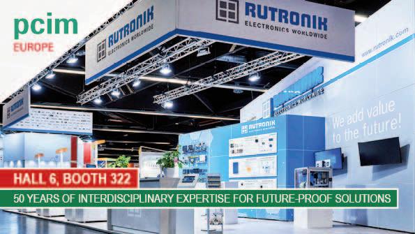
Every new application has the potential to shape progress and the current transformation. Whether in the areas of Industry 4.0, autonomous driving, eMobility, or IoT – almost every new technology requires energy and underscores the importance of power electronics. That development is also evident at Rutronik’s booth at PCIM Europe (May 911, 2023). In Hall 6 at Booth 322, the broadline distributor presents state-of-
the-art components from leading manufacturers through forward-looking complete solutions from the power and sensor technology sectors. Rutronik’s experts aim to develop the best possible solution for the respective application and have done so already for 50 years.
For five decades, Rutronik and its partners have supported customers in the development of forward-looking solutions and have offered advice. At ten counters at PCIM Europe in Hall 6, Booth 322, the experts provide insight into the latest trends in power electronics and sensor technology.
The focus is on components from wellknown manufacturers and solutions relating to Energy Management, Connectivity, Smart Metering, and alternative Drive Systems. In the power segment, visitors can look forward to product highlights from the manufacturers Infineon, Littelfuse, ROHM, RECOM, Toshiba, ELMOS, and Samwha. Products from the manufacturers TDK, Sensirion, Murata, and Omron show up in the sensors sector.
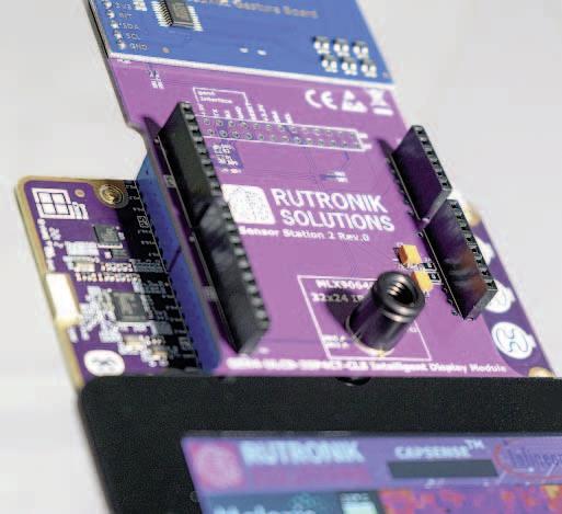
In addition, the experts from Rutronik System Solutions introduce the complete board family consisting of Base and Adapter Boards. The latest member of the family – the RDK3 – which offers a unique approach to the development of ultra-low power Bluetooth applications, is also presented. For all Base and Adapter Boards, only components are used that are also available in Rutronik’s product portfolio.
“The demand for efficient approaches to energy supply and electromobility is constantly increasing. Our customers benefit from our 50 years of expertise and broad portfolio, including power and sensor components, to help shape this change with your application”, says Andreas Münzer, Senior Manager Product Marketing Power at Rutronik Elektronische Bauelemente GmbH. “Together with our partners, we support the ongoing transformation in the areas of energy management, connectivity, smart metering, and alternative drive systems.”
MicroSys Electronics announces a new evaluation kit for its miriac System-onModules based on NXP Semiconductors S32G processor family. Deployed in vehicle networks as headless controllers, these highly integrated and performance scalable processors support ADAS and other functions for increasingly autonomous vehicles.
Developers can use the new miriac evaluation platform, which is designed as a modular single board computer (SBC), to test the performance balancing of their applications and to connect their CAN-, LIN-, FlexRay- and 100BASE-T1-based peripherals via automotive connectors. The evaluation kit includes NXP S32G274A and/or new NXP S32G399A based miriac System-on-Modules, a carri-
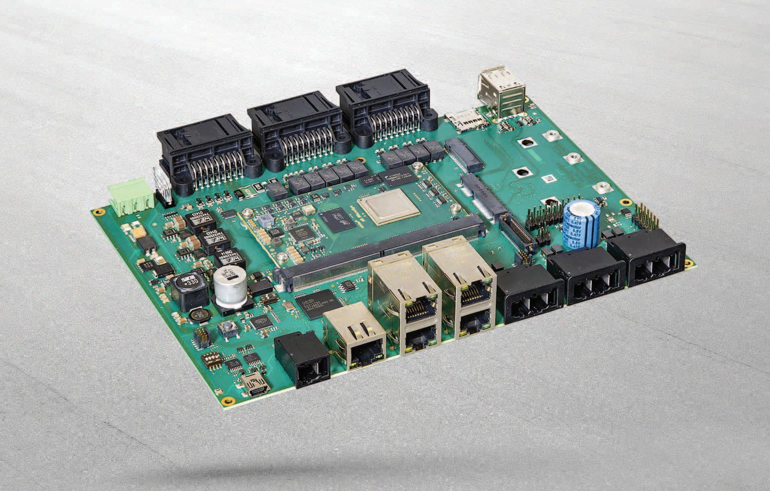
er board in the shape of a dedicated modular SBC, as well as the appropriate power supply, cable sets and a pre-installed Linux image.
Developers of mixed-critical safety applications benefit from up to eight Arm Cortex-A53 cores and four Arm Cortex-M7 dual-core lockstep pairs. This is sufficient to process LiDAR and video data alongside functionally safe vehicle control.
When extended with one or two Hailo-8 AI processor modules, the evaluation kit also provides numerous pre-trained computer vision models for situational awareness. OEMs using such application ready System-on-Module based platforms – for which MicroSys also develops certification
ready system designs – gain access to rapid prototyping, advanced connectivity for their specific use cases, comprehensive software support, and documentation required for safety certification up to ASIL D. Target markets are real-time connected and increasingly autonomous vehicles, all types of mobile machines, as well as automotive test and measurement equipment.
The new miriac SBC-S32G399A based evaluation kit is available now.
For more information, please visit: https://www.microsys.de/en/products/s bc/arm-architecture/miriacr-sbcs32g399a/
MicroSys Electronics
https://microsys.de


Technologies are finally getting to a level where advancement in system deployments are allowing robots to become more real time environmental aware. Driving this technology era, where sensors, integration and compute units are powerful enough to enable more advanced system architectures, allow new and much more scalable autonomous robotic designs.
Together, this enables a more streamlined manufacturing methodology enabling smarter and more flexible robotic cell deployment, supporting higher level market and legislative demand for better and even more sustainable production flow. During this article, the technology enhancement of these sensors, fusion integration, and deployment methods, will be discussed with the overarching real-time environmental awareness theme. All in all, capturing how a more flexible and scalable production deployment will evolve robotic integration and design thus advancing going forward.
The Challenge – impacted by growth in global supply demand, regionally changes and labor shortage, more organizations are advancing in smarter and more flexible manufacturing installations
to make production cost-effective, more scalable, and efficient. However, due to the global impact of the COVID-19 pandemic and changing economic climate, these efforts have been slowed. In fact, nearly half (49%) of manufacturers have delayed current smart manufacturing implementations because of these two impacts. The concept of smart and more flexible manufacturing is an innovative approach to optimize production flow with the use of robots, sensors, and other advancements for automating parts of the complete manufacturing process. This inherently defines, the sub systems and implementation structure of the factory and are opening a new playbook for how to define, design and implement robotic systems, robotic cells, and their integration into the manufacturing floor. There are many specialized tasks in the overall
process that require accurate monitoring of all systems installed. Not only simple sensing units like pressure, temperature and flow are quantified but now also, environmental perception, localization of mobile systems, real-time optimization of installed robots manufacturing performance and machine to machine communication. All put in place to ensure highest throughput, throughout the complete manufacturing process.
The scalable solution – Integration and installation of robotic systems are, heavily depending on which functionality and capability are needed for the given manufacturing flow. How the layout and build of the factory has been defined and architected to support the required manufacturing process. The robotic ecosystem including sensor, motor, drives, tool makers and
many more has been pushing toward a more open source and easy installation methodology over the last years. This push in combination with more advancement in processing performance and better real time connectivity, in a safe manner, are now enabling this methodology.

The base technology providers have developed and adopted higher performance technologies, supporting simplified higher data throughput from the analog to digital domain in core and modular sensor deployment. This integration is enabling more advanced middleware to run either at the edge, or in more centralized compute units using higher performance interconnectivity like GMSL (Gigabit multimedia serial layer), or other high performance communication medias.
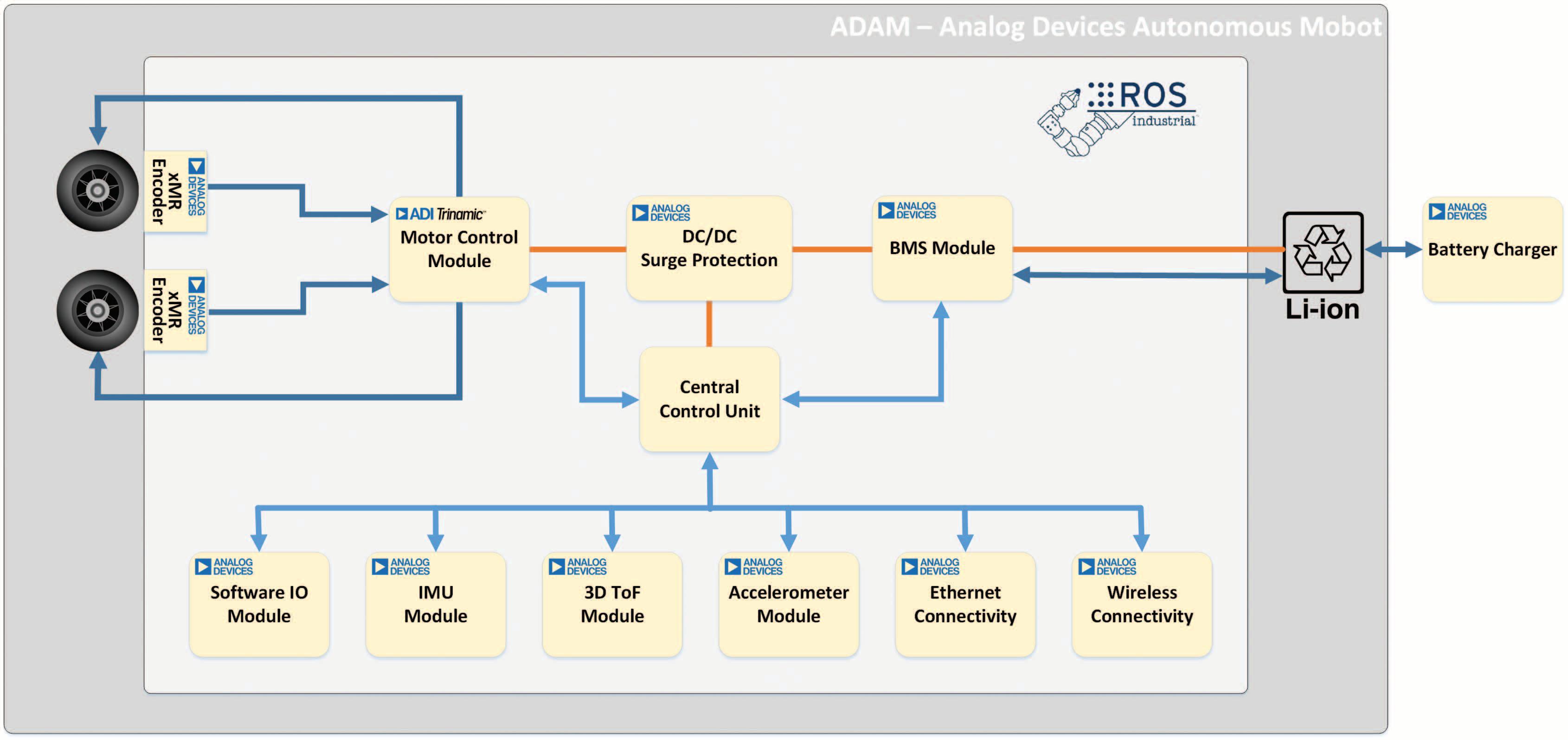
Looking at the block diagram below a high-level representation of the core modules in an autonomous system has been highlighted.
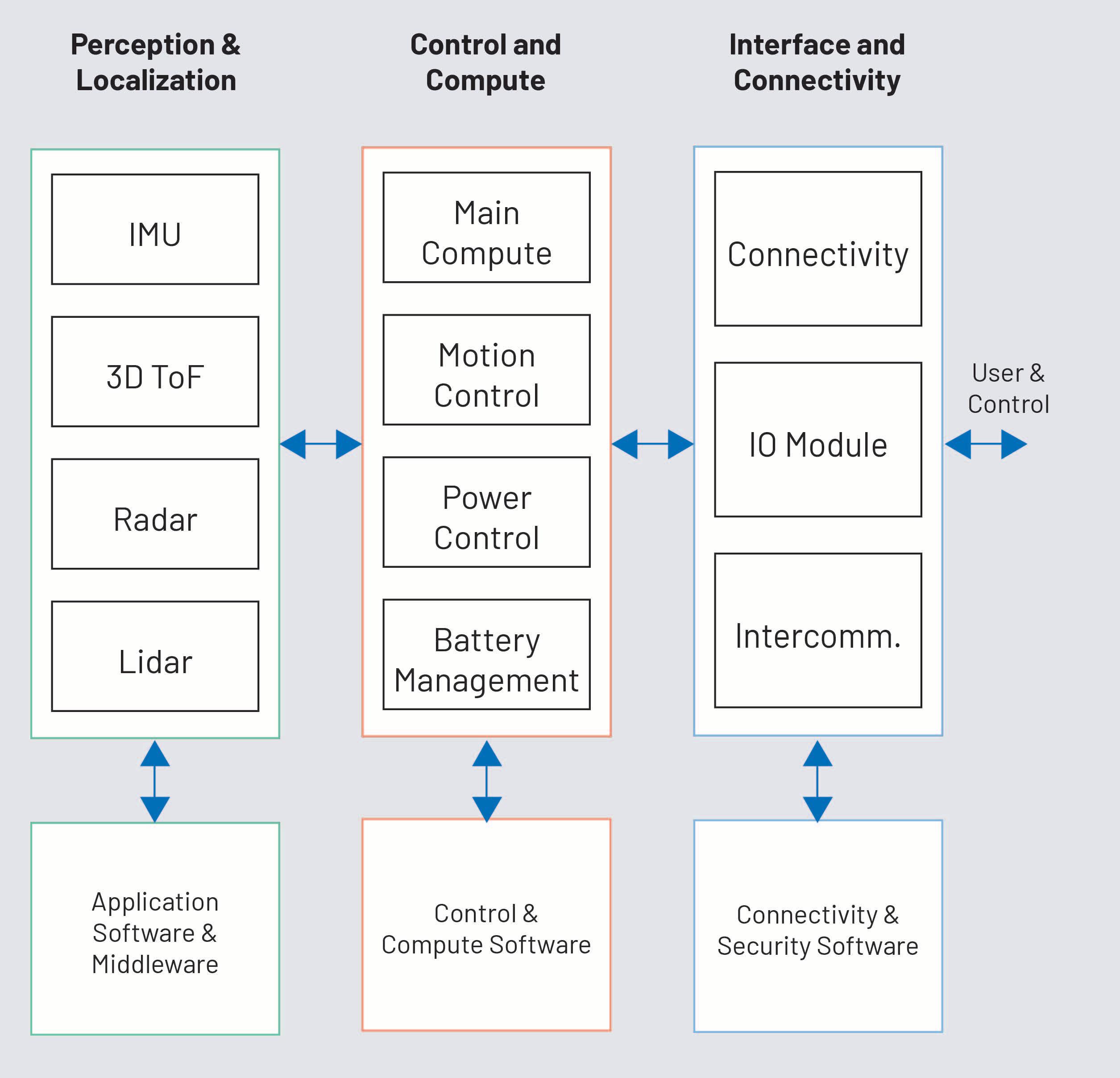
Each of the modules representing an intelligent sub-system, capable of delivering real time data from sensor or interface to the main control units.
These blocks are created in a fashion that natively embrace open-source deployment and in most robotic system would be deployed with ROS (Robotic Operating System), as the main software interface between each of the nodes in the system. The ROS community has lately been focused on advancing both the real time aspect in deployment including enhancement beyond sensor technologies into more complete system aspects as far as security and safety. the mixed-signal device.
functionality beyond normal defined output, expanding the total knowledge of the system beyond none fused systems.
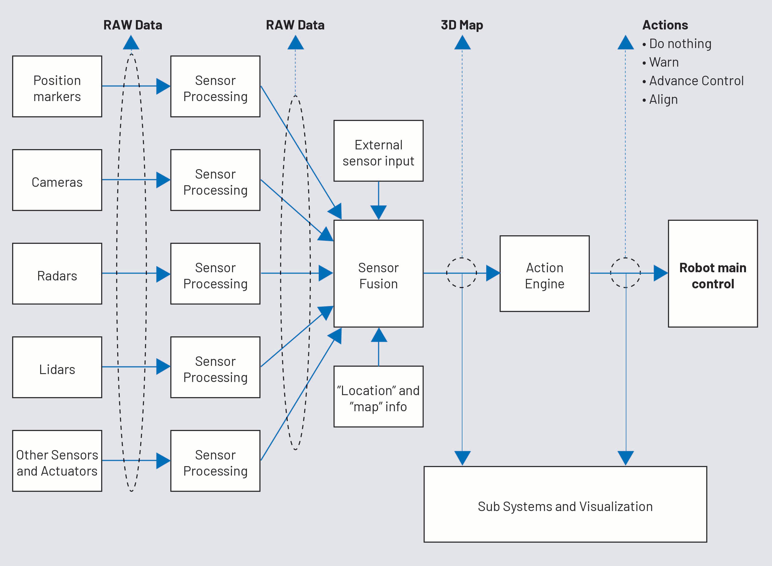
Modular perception and advanced sensor fusion – Sensor fusion done in a real time environment, adds value in both visualization, mapping and control loop for the robotic engine and bring benefits directly into a more precise and real-time aware controlled system.
As an example, by fusing perception (Camera, Radar, etc.), actuator information and localization data it is possible to optimize the mapping path for autonomous robots without losing information and trusted data for the functionality of the manufacturing robot. This sensor combination continually enhances and expand the functionality for the autonomous system and will in many cases maximize the sensor
One method of implementation of sensor fusion is a class of Kalman Filters, which models the current and previous state of the robotic system based on with real time measurement and prediction. In case where false information are applied, tampered, into the sensor system the architecture can be enhanced by using techniques in combination with machine learning and neural networks creating a higher level of security and data protection. Sensor fusion increases the system integrity, reliability, and robustness in controlled real-time operations and provides additional benefits against sensor network attacks originating from the analog domain. By implementing sensor fusion into the systems, designers and architects can mitigate the risk from malfunction or malevolent action that can cause injury to people or property.
Another value in doing sensor fusion is that data can be used for multipurpose to enhance other sensor or data information to a given format.
Allowing the designer to optimize the data paths and functionality of a give system, but also reuse the sensor modules in a fashion that best suit the use case and deployment method.
approach to the individual elements in the system, and by having ROS interfaces for them. This enables the modules to interconnect and inter-operate easily, while also enabling the designer to take advantage
(perception) at high-speed data output to enable true real-time depth information. (2) IMU modules that incorporate trusted data paths for localization and guidance, in combination with (1), the perception module, to enable SLAM and full navigation.
From the motion / movement perspective (3), Analog Devices’ motor control division “Trinamic” has a large set of individual modules facilitating smooth drive and control of motor systems supporting drive of each wheel. Specifically in harsh and changing environment, using sensor fusion of vision, localization, motor position and movement, now allowing SLAM, still to be carried out even with some missing set of data from individual sensors. (4)
As can be seen above, raw data can be taken out of the system independently and correlated with compressed and already existing data to create the correct and/or corrected dataset out of the action engine. All in all, the optimized data will have one purpose, create a faster and more intelligent system allowing the robot to move more self-aware and perform more optimized decisions based on the perception and sensor impression. Analog Devices has a large set of system-, application-, and software- modules, where the individual optimization paths for different sensors are designed for multipurpose use-cases and end applications. Overall, these types of fusion system are expanding the functionality and real time capability of the autonomous systems, benefitting the manufacturing setup with a lower total operating cost through better optimization, even resulting in cases where the sensor fusion enablement, will allow remote operation from control-centers, to drive the smarter factory toward higher level of sustainability and economic prosperity.
Taking the above approach and deploying it on a real autonomous robotic system is greatly facilitated by taking a modular
of the open-source software and applications modules such as those developed for SLAM (Simultaneous localization and mapping), and simulation environments such as RViz (ROS visualization). Typical modules for navigation consist of (1) a camera frontend (3D-ToF), where the 1MPix quality imager enhance the overall depth mapping
The power combination is covering both the DC/DC for the local POL and the BMS supporting battery balancing and cell monitoring, enabling transparency of battery consumption and health. (5) Other sensors, interfaces, accelerometers, wireless transceivers, ethernet connectivity are also deployed in the platform, these are end-system and specialized sub-modules and can be added as extra features (nodes) to the overall platform where needed.
In the pictuire below, Analog Devices’ ADAM (Analog Devices Autonomus Mobot) are shown in physical form and with the high level modular archectecure of the autonomus robot.
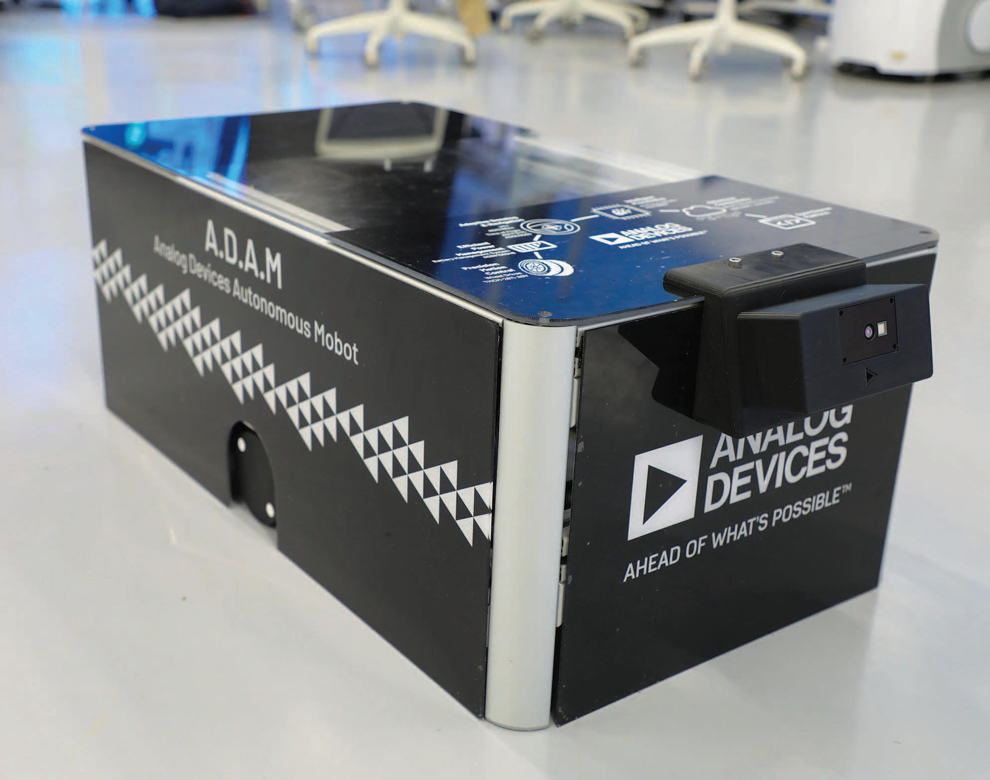

Each of the modules are connected in realtime, supporting sensor and modules to enable autonomous guided driving functionallity. ROS has been used to enable ease of configuration and scalablity, supporing the overarching modular design theme as already mentioned.
Bridging technologies from silicon implementation to modular deployment – during this article it has been discussed how to improve and advance deployment of autonomous and advanced robotics. From an academic point of view, it will always be possible to use and implement systems towards optimal performance, however in a full manufacturing and optimized solution, total cost of deployment and functionality matters to an extent only the end user and controller has in mind. Analog Devices has due to this paradigm, expanded their solution focus by bringing together the academic world, innovators, partners, and customers along with Analog Devices core and module technology in a creative innovation center in Ireland, Limerick.
This center, named Catalyst, is forming a new standard for co-creation and development of advanced system design, not only at a standard component and system level, but also learning from the ecosystem requirements and bringing system and modular designs to a new era of integration. The Design Center, Catalyst, will embrace new standards for how
Analog Devices are enabling designs supporting more advancement in areas of sensor fusion, intercommunication in a fashion that secures even more flexible and sustainable production facilities in the future. For more information about how Analog Devices are enabling this new robotic era, please go and visit analog.com/robotics.

■ Analog Devices www.analog.com

Engage with like-minded members and ADI technology experts in our online community, EngineerZone®. Expand your network, ask your tough design questions, share your expertise, browse our rich knowledge base, or read about new technologies and the engineers behind them in one of our blogs.

Visit https://ez.analog.com
https://ez.analog.com

Modern communications and sensing technologies have revolutionized the way cars are designed. To increase safety and move towards autonomous driving, new vehicles must include systems that can interact with their surroundings, infrastructure, or other traffic participants to detect possible sources of danger. Automotive sensors are therefore key to improving road traffic safety and reach high levels of autonomous driving. Their use will help reduce the number of traffic accidents and deaths on the roads worldwide, with the final objective set by Vision 0: Zero deaths in traffic accidents by 2050.
Author: Marta Martínez-Vázquez Senior Staff Product Marketing Engineer − Automotive Analog Product Marketing Division Renesas Electronics Europe GmbH
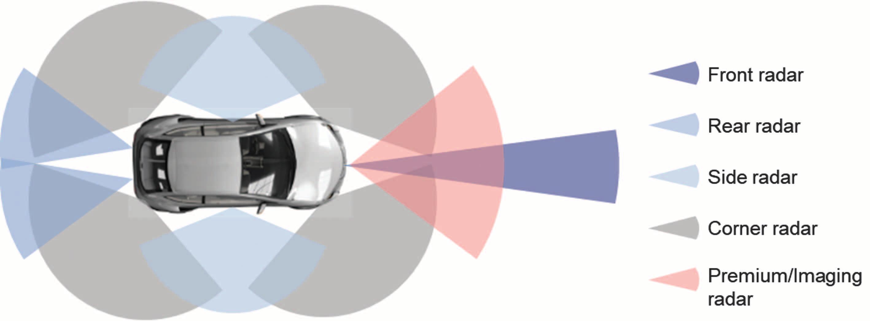
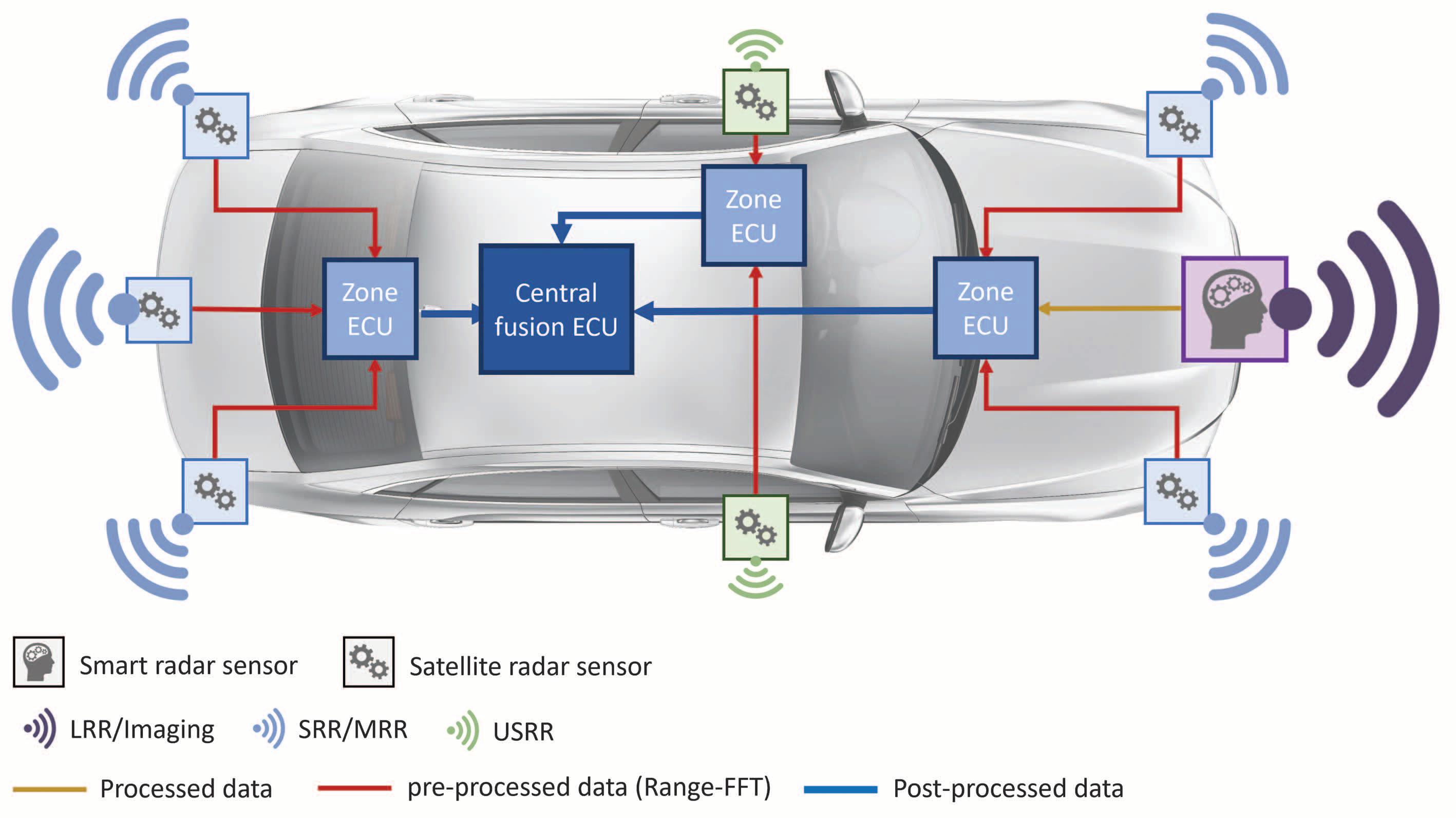
Among the sensors that are considered for assisted and autonomous driving, radar has proved to be extremely reliable for ADAS applications such as adaptive cruise control. Applications for radar are expected to expand in the future, as radar is often used together with other sensing technologies such as video cameras and lidar. The advantages and drawbacks of the different sensor types are summarized in the table below. Full autonomous driving will most likely require the fusion of data obtained from different sensing technologies. With sensors distributed around the car, it will be possible to provide full 360° coverage, creating a safety “cocoon” around the car. Figure 1 illustrates the concept when only considering radar sensors.
Optical imaging Large field of view.
CONS
Limited by weather and light conditions.
(video) High resolution. High processing workload.
Ultrasonic Operation in all weather & Very short range. light conditions. Very low cost.
Infrared Operation in low light conditions. Short detection range.
LiDAR High accuracy
Limited by weather conditions (fog, snow).
(range, resolution & position). No direct information about velocity.
Radar Less sensitive to weather Complex angle measurement. conditions. Complex target classification. Long detection range. Not mature for fully AD. Good resolution and position estimation.
Pros and cons of different sensor technologies for automotive applications
An additional advantage of radar is that radar sensors can easily be installed behind common elements of the car, like bumpers or emblems, so that they are invisible and do not affect aesthetics. The frequency band from 76 GHz to 81 GHz has been accepted by most countries as the frequency band for automotive radars. The physical integration gets easier with high frequencies of operation, as the size of the radar antennas will be reduced. Yet new challenges appear when going up in frequency, due to tradeoffs in power, higher losses, and higher impact of manufacturing tolerances.
Radar is also especially suited for automotive applications, as vehicles are good reflectors for the radar waves. It can be used for both “comfort” functions such as automatic cruise control, but also for highresolution sensing applications, which add
to the passive and active safety of a vehicle. Examples include blind spot detection, lane-change assist and rear-traffic-crossing-alert, detection of pedestrians and bicycles near the vehicle. Nowadays, radar sensors can be classified based on their detection range, as shown in figure 2 below.
• Short Range Radar (SRR): up to 50 m with wide field of view and high resolution
• Mid-Range Radar (MRR): up to 100 m with medium field of view
• Long Range Radar (LRR): 250 m or more range, with narrower field of view and less focused on resolution
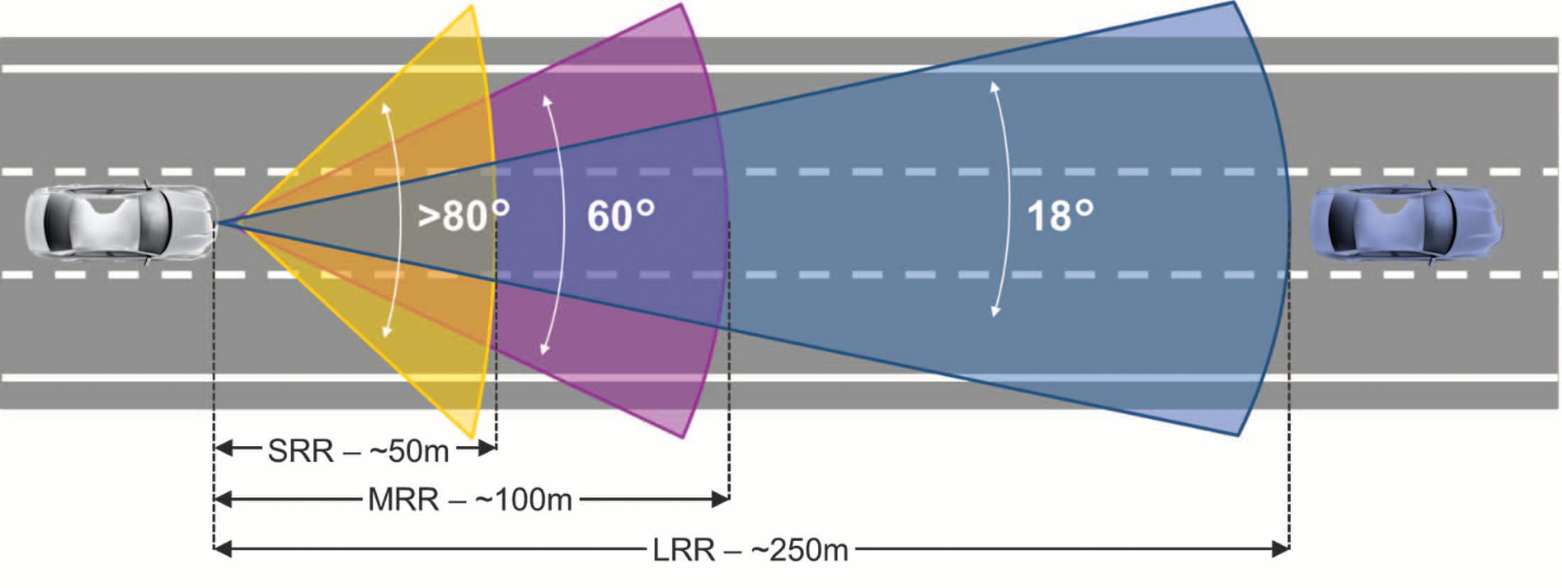
With new technology development, the range is expected to extend beyond these limits, while the vertical dimension
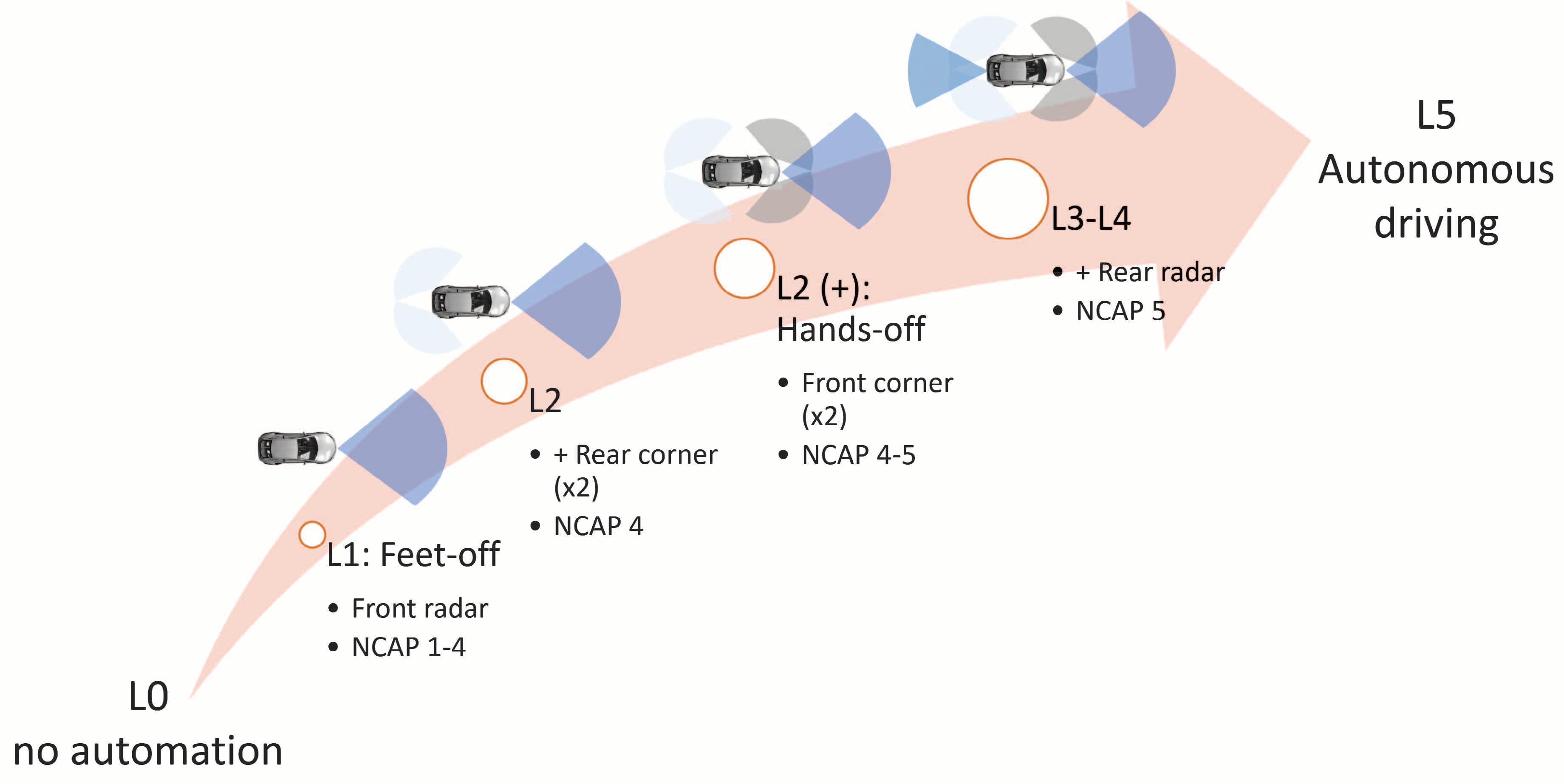
is added to the detection, to provide a full 3D image of the surroundings. In the future, multiple radar modules will be added to cars, to move from a basic forward-looking radar configuration which provides basic Level 1 autonomous driving to Level 4 in the NCAP (new car assessment program). Soon more cars will be equipped with corner radar sensors to reach Level 2+ autonomous driving and NCAP 4-5 in standard cars, and Level 3-4 in autonomous driving and NCAP 5 for the premium segment (figure 3).
Yet, the way the radar data will be handled will strongly depend on the vehicles’ architecture. The current trends towards increased performance of the central computing units are also driving an evolution of in-vehicle E/E architecture to shift to a distributed architecture.
Although the migration to a fully distributed architecture will not be completed until the 2030s, partial implementations will appear in the market earlier. First, some domain controllers will be used for specific functions such as ADAS. Then the number of domain controllers will increase, while zone controllers will also be introduced along before a fully centralized E/E architecture is established, in which the vehicle central computer will be connected to the sensors through the zone control units. This evolution will also require increasing the capacity and reliability of the vehicle’s networks, and well as the software complexity.
With the new E/E architectures being introduced, part of the radar processing could be offloaded from the radar sensor module (edge computing) to the zone or the central ECU, allowing for more efficient computations. Today, the full radar processing is carried out on the edge, with “smart sensors,” as shown in figure 4 below. This means that a number of independent radar modules are distributed around the vehicle, each of them with their own transceiver and processing capabilities. The processed data, normally the object list, is then transferred to an ADAS ECU for further processing, and,
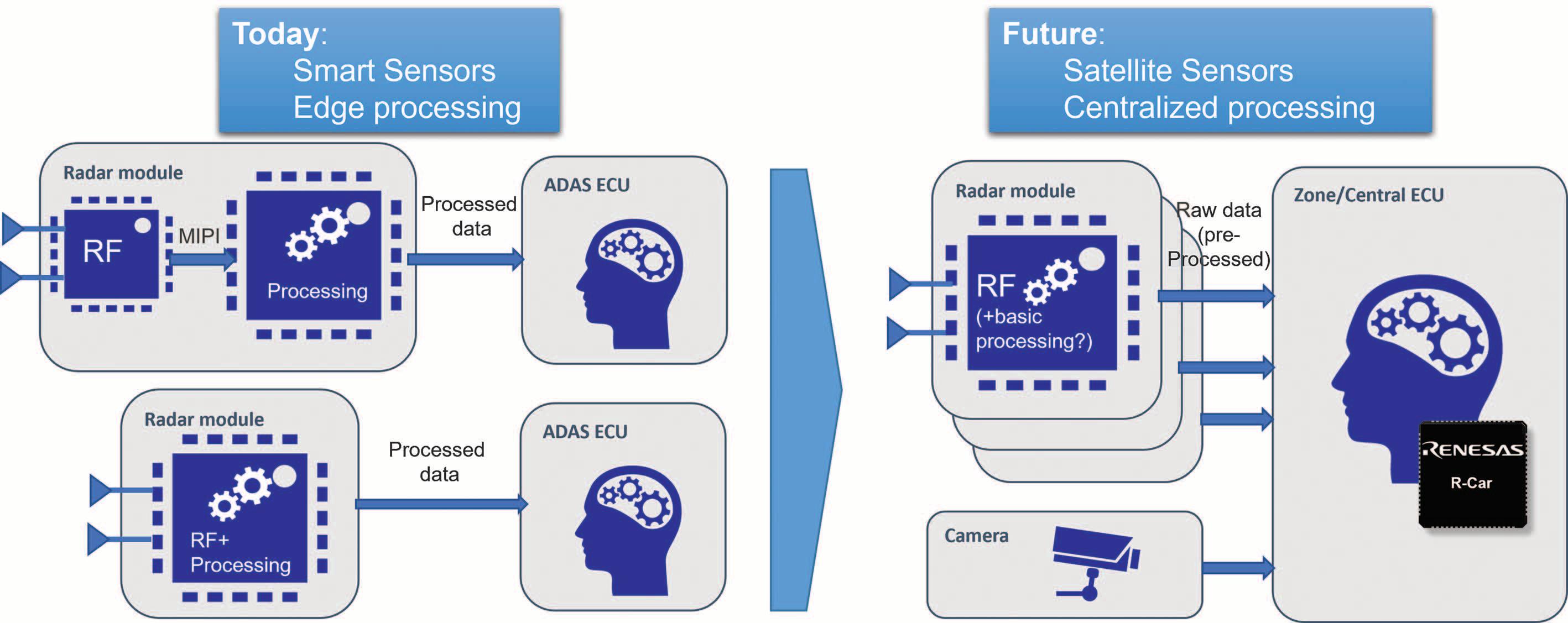
potentially, fusion with the data from other sensors. With appropriate distribution of sensors in the car, the environment of the vehicle can be properly perceived, and obstacles can be identified. With the development of centralized computing architectures, the processing of the data from some radar modules will probably be shifted from the radar sensor to a remote processing unit, either a zone ECU or the vehicle’s central computer directly. The radar modules themselves would then be less “smart” and perform only a limited amount of processing of the received radar signals.

For example, the module will determine the distance to the different objects and provide the range profiles to the remote processor. It will then receive the preprocessed data from different satellite radar modules and perform the remaining processing steps for each set of data, to generate the object list with their respective characteristics (distance, direction, and velocity), to create the full image of the surroundings. The obtained results will then be fused together or combined with the results obtained from other sensors. This new, multi-sensing configuration will provide the required accuracy and eliminate redundancies to enable high levels of autonomous driving, as shown in figure 5 above.
In the first implementations of this centralized architecture, the pre-processed from the different radar sensors can be transferred to zone or central ECUs using the car’s Ethernet backbone. When higher definition is needed and the amount of radar is too large, as in the case of forward-looking or imaging radar, the radar processing may still be carried out on the sensor itself, to reduce the amount of data to be transferred.
Centralized processing of data from remote radar sensors offers a wide range of benefits.
Firstly, the radar modules themselves become less complex, thus saving size and cost, and reducing heat dissipation problems. Reparations and upgrades, both for hardware and software, become easier.
Secondly, using the existing network of the car, namely the ethernet backbone, also reduces the costs and weights for cabling. Additionally, the data transferred through Ethernet will be available in a format which makes them easier to store and work with.
Finally, processing the data on the vehicle’s control units opens the door for higher efficiency and more sophisticated and complex operations. The sensing capabilities can be enhanced by implementing data fusion with the information obtained from other sensing technologies, such as cameras or lidar. Machine learning and artificial intelligence can be considered for advanced detection and prediction, thus allowing for higher levels of autonomous driving.
Both edge processing and centralized computing are expected to coexist for some years. The migration to E/E architectures with centralized computing will require access to high-speed links throughout
the vehicle, which may lead to the use of different standards for data exchange. In any case, additional security measures become necessary to guarantee the integrity and security of the transferred data. The increased number of radar modules on the car itself and on other vehicles, all of them transmitting and receiving radio waves, can also lead to interference problems that will need to be solved.
Renesas is working towards providing cutting edge solutions for future vehicles.
Renesas has just presented its first millimeter-wave radar transceiver for automotive, the RAA270205, to expand its sensing solutions for ADAS. Renesas aims to provide innovative components for the radar modules with radar transceivers for imaging, centralized processing, and imaging applications, coupled with ECUs based on the R-Car Gen4 series.
■ Renesas www.renesas.com

This article briefly outlines the benefits of cellular IoT before explaining the design complexities that the technology can introduce. The article then describes how the use of cellular IoT development boards can eliminate much of this complexity. Finally, the article describes how to set up a Microchip Technology development board to send simple color and temperature data to the cloud.
Author: Rolf Horn | Applications Engineer Digi-Key Electronics
Cellular Internet of Things (IoT), a low power wide area network (LPWAN) technology, offers a clear and proven path to secure and robust IoT for applications ranging from smart cities to agriculture, and remote infrastructure monitoring. However, cellular IoT is a complex technology, daunting for inexperienced designers embarking on a project. However, cellular IoT design challenges can be eased by basing projects on cellular development boards which use familiar general-purpose microcontrollers (MCU) and integrated design environments (IDEs). Backed up by libraries of
open-source software and simple sensor connection, these development boards make it easier for the designer to get started with cellular IoT projects from hardware layout all the way up to sending data to the cloud.
What is cellular IoT?
Cellular IoT uses low-power cellular technology to connect IoT end devices (such as sensors and actuators) to the cloud. It is an LPWAN technology characterized by kilometer-plus range, high-density enddevice support, and low throughput. While other LPWAN technologies exist
notably LoRaWAN (see, “Accelerate LoRaWAN IoT Projects with an End-to-End Starter Kit” and Sigfox cellular IoT offers some key advantages, including:
• Future proofing: As a standard, the specification for cellular IoT is constantly under review and development.
• Scalability: Cellular IoT can support the rapid deployment of IoT through established cellular architecture.
• Quality of Service (QoS): Cellular IoT offers high reliability because it’s based on infrastructure that’s proven and mature in high-volume commercial applications.
• IP interoperability: End devices can be directly connected to the cloud without the need for expensive and complex gateways.
Designers need to factor in that with cellular IoT is there is an ongoing expense associated with data transfer. This is not the case with competing technologies such as LoRaWAN which use the unlicensed frequency spectrum. However, cellular IoT data costs are trending down due to competitive pressures and increased use of edge computing, reducing the volume of unremarkable data sent across the network.
Cellular IoT is governed by a telecom standard regulated and updated by the Third Generation Partnership Project (3GPP). Release 13 of the 3GPP’s standard extended its machine-to-machine (M2M) modem categories to allow for low-cost, lowpower, and low-throughput modems suitable for IoT connectivity. Further releases to the standard have resulted in further enhancements to these IoT modems. Wireless sensors equipped with cellular IoT modems can send data across kilometers to the cloud without the need for expensive and complex gateways, along with the security and QoS for which cellular is known.
The difference between
LTE-M and NB-IoT
Cellular IoT comes in two forms, LTE category M1 (LTE-M) and narrow band IoT (NBIoT). Both types are designed for use with resource-constrained, often battery-powered devices that are typical of the IoT and Industrial IoT (IIoT). Because IoT modems connect to established cellular infrastructure, each requires its own subscriber identity module (SIM).
LTE-M is based on stripped-down LTE (“4G”) technology. It supports secure communication, ubiquitous coverage, and high system capacity. Its ability to operate as a full-duplex system over a relatively wide bandwidth (1.4 megahertz (MHz)) improves latency and throughput compared with NB-IoT. The raw data throughput is 300 kilobits per second (Kbits/s) downlink and 375 Kbits/s uplink. The technology is suitable for secure end-to-end IP connections, and mobility is supported by LTE cell handover techniques. LTE-M is suitable to mobile applications such as asset tracking or healthcare.
NB-IoT is primarily designed for energy efficiency and for better penetration into buildings and other RF unfriendly areas. Unlike LTE-M, it is not based on the LTE physical layer (PHY).
Modem complexity is even less than that of an LTE-M device, as NB-IoT uses a 200 kilohertz (kHz) bandwidth. While raw data throughput is a modest 60/30 Kbits/s, range is better than LTE-M. NB-IoT is suited to static applications such as smart meters that might be obscured by walls.
A range of commercial LTE-M/NB-IoT modems is now available. One example is the Monarch 2 GM02S module from Sequans. The device supports a single stock keeping unit (SKU) RF front-end suitable for 20 of the global LTE bands.
The modem is designed solely to look after communication between the end-device and the base station. A separate supervisory and application processor is needed to control the modem while also running the sensor application software. In addition, the designer also needs to consider the antenna circuit(s), power supply, and equipping an end-device with a SIM to ensure seamless connectivity with the cell network (see, “How to Use Multiband Embedded Antennas to Save Space, Complexity, and Cost in IoT Designs”. Beyond the hardware design, some coding skills are needed to get a cellular module to connect to the network and receive/ transmit data. If the design uses an external application MCU, it typically communicates with the cellular module using a UART serial link (although other I/O interfaces are also used).
AT (“attention”) commands are the standard means of controlling a cellular modem. The commands comprise a series of short text strings that can be combined to produce operations such as dialing, hanging up, and changing the parameters of the connection.
It is supplied in a compact LGA module measuring 16.3 × 17 × 1.85 millimeters (mm). The module meets the requirements of 3GPP Release 14/15. Powered from a single supply of 2.2 to 5.5 volts, the modem is capable of a maximum transmit power of +23 decibels referenced to 1 milliwatt (mW) (dBm).
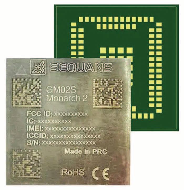
The GM02S supports an external SIM and eSIM as well as integrated SIMs. A 50 ohm (Ω) antenna interface is included. The device is supplied with an LTE-M/NB-IoT software stack and Sequan’s Cloud Connector software for ease of connection to commercial cloud platforms (Figure 1).
While the GM02S modem is a highly integrated device supplied with a software stack and cloud connectivity, like all commercial modems, there is still considerable development work required before an IoT application is seamlessly sending data over kilometers to the cloud.
There are two types of AT commands: Basic commands are those that don’t start with “+”. “D” (Dial), “A” (Answer), “H” (Hook control), and “O” (Return to online data state) are examples. Extended commands are those that do start with “+”. For example, “+CMGS” (Send SMS message), “+CMGL” (List SMS messages), and “+CMGR” (Read SMS messages) (see “Use a Cellular Module to Connect a Maker Project to the IoT”.
These hardware and software considerations bring complexity to cellular IoT that could slow progress with less-experienced designers. Fortunately, application MCU and cellular IoT modem makers have now gotten together to offer hardware and software design tools that make it much easier to take advantage of this important LPWAN technology.
Tackling the challenges of cellular IoT design is considerably eased by basing a prototype on a purpose-designed development board. The development board hardware typically includes an antenna, a power source, a SIM with some free data allowance, an application processor, and tuning networks to ensure good RF performance.
This gives designers a solid hardware head-start for their project and allows them to focus on application development. With the right choice of development board, the application development can even be conducted in a familiar IDE.
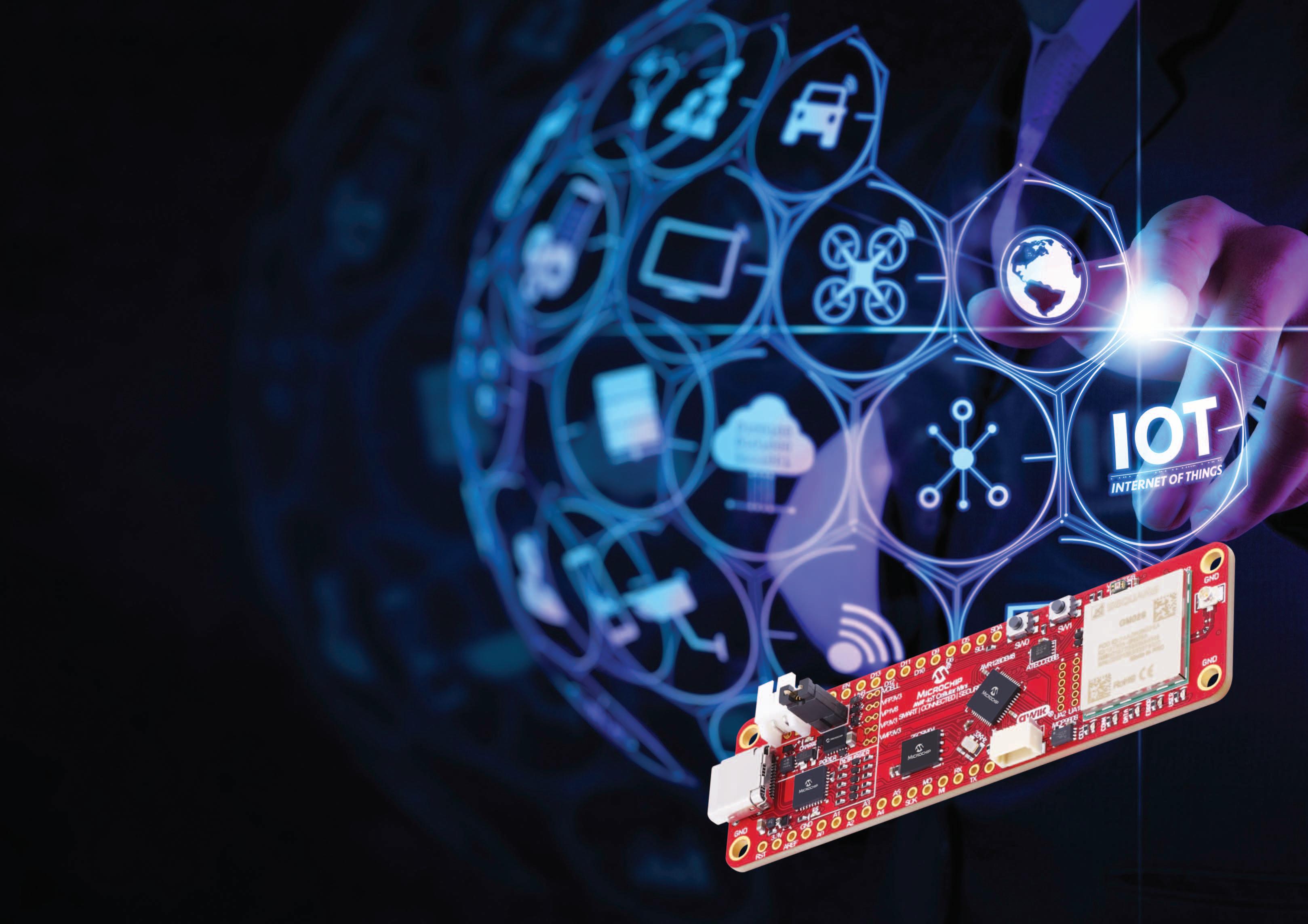
One example of a popular cellular IoT development board is the EV70N78A AVRIoT Cellular Mini Development Board from Microchip. This is a hardware platform based around the popular Microchip AVR128DB48 MCU, and the Sequans Monarch 2 GM02S cellular module detailed above. The MCU is an 8-bit, 24 MHz device. It has 128 kilobytes (Kbytes) of flash, 16 Kbytes of SRAM, 512 bytes of EEPROM, and comes in a 48-pin package.
The development board also integrates an ATECC608B; secure element; once connected to an LTE-M or NB-IoT network, the ATECC608B is used to authenticate the hardware with the cloud to uniquely identify every board. To make things even easier for the designer, the Microchip development board also includes an activation-ready Truphone SIM card with 150 megabytes (Mbytes) of data.
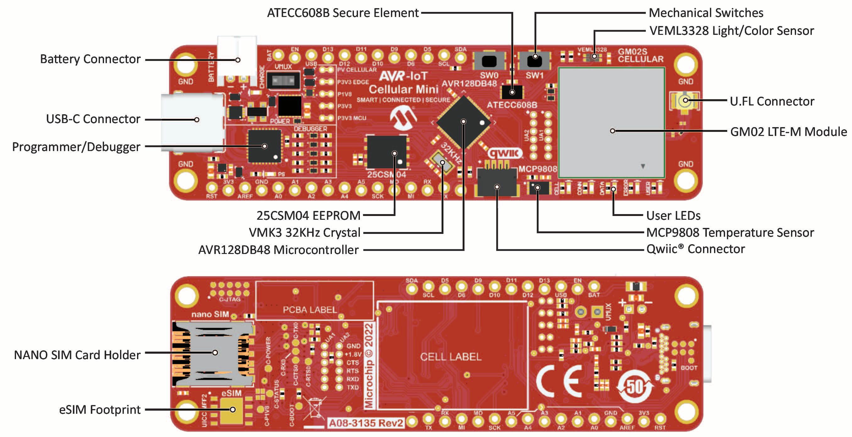
The development board features five user LEDs, two mechanical buttons, a 32.768 kHz crystal, color and temperature sensors, an Adafruit Feather compatible edge-connector, a Qwiic I2C connector, an on-board debugger, a USB port, battery and external input power options, and an MCP73830 Li-ion/Li-po battery charger with charge status LED (Figure 2).
Starting a cellular IoT project
The purpose of cellular IoT is to wirelessly connect IoT end-devices such as sensors and actuators so their data can be sent over kilometers to the cloud. On the Microchip development board, the MCU is preloaded with a firmware image forming a demo application that lets users quickly connect and send data from the onboard temperature and color sensors to a cloudbased sandbox (hosted by AWS).
To get the hardware ready for development, it’s simply a case of activating and inserting the SIM card, connecting the external antenna to the board, connecting
the debug USB-C port on the board to the PC, scanning the QR code on the bottom of the board or opening the massstorage device, and following the CLICKME.HTM to the kit web page.
A Microchip IoT Provisioning Tool, available from Github, provides an easy-touse solution for configuring an AVR-IoT Cellular Mini to the selected cloud provider, setting the network provider, and selecting cellular frequency bands. (For the sandbox demo firmware to work, the development board must be provisioned for the AWS Microchip sandbox.)
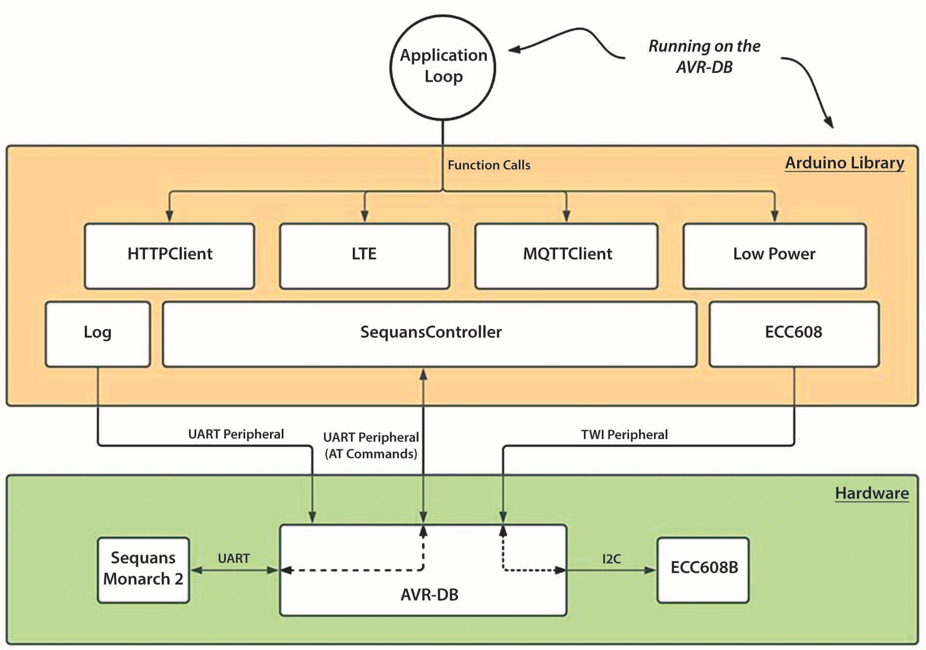
Once developers have gained some confidence with the demo application, they can start to build their own application using the development board’s full Arduino IDE support. This support is based on an AVR IoT cellular Arduino library hosted on Github. The library is built on top of the open-source DxCore (Figure 3).
The on-board debugger (PKOB nano) supplies full programming support for the Arduino IDE. There’s no need for any external tools, and it also provides access to a serial port interface (serial-to-USB bridge) and two logic analyzer channels (debug GPIO). The on-board debugger on the AVR IoT Cellular Mini board appears as a human interface device (HID) on the host computer’s USB subsystem. For more ambitious projects, the development board’s Qwiic and Feather compatible
edge connectors allow for easy expansion from a wide selection of add-on boards from Sparkfun and Adafruit (Figure 4).
On the Microchip development board, power to all the board parts is connected through five cut-straps.
4 Run a single-ended analog-to-digital conversion (ADC).
5. Calculate the voltage using the equation: V = ADC result × VREF × 4/ADC resolution.
Finally, it is also simple to measure the supply voltage by following these steps:
1. Configure the voltage reference for the ADC.
2 Select VDD or VDDIO2 as the positive input to the ADC. (VDD and VDDIO2 are available internal input channels to the MCU’s ADC.)
3 Run a single-ended ADC conversion.
4 Calculate the voltage using the equation: V = ADC result × VREF × 10/ADC resolution.
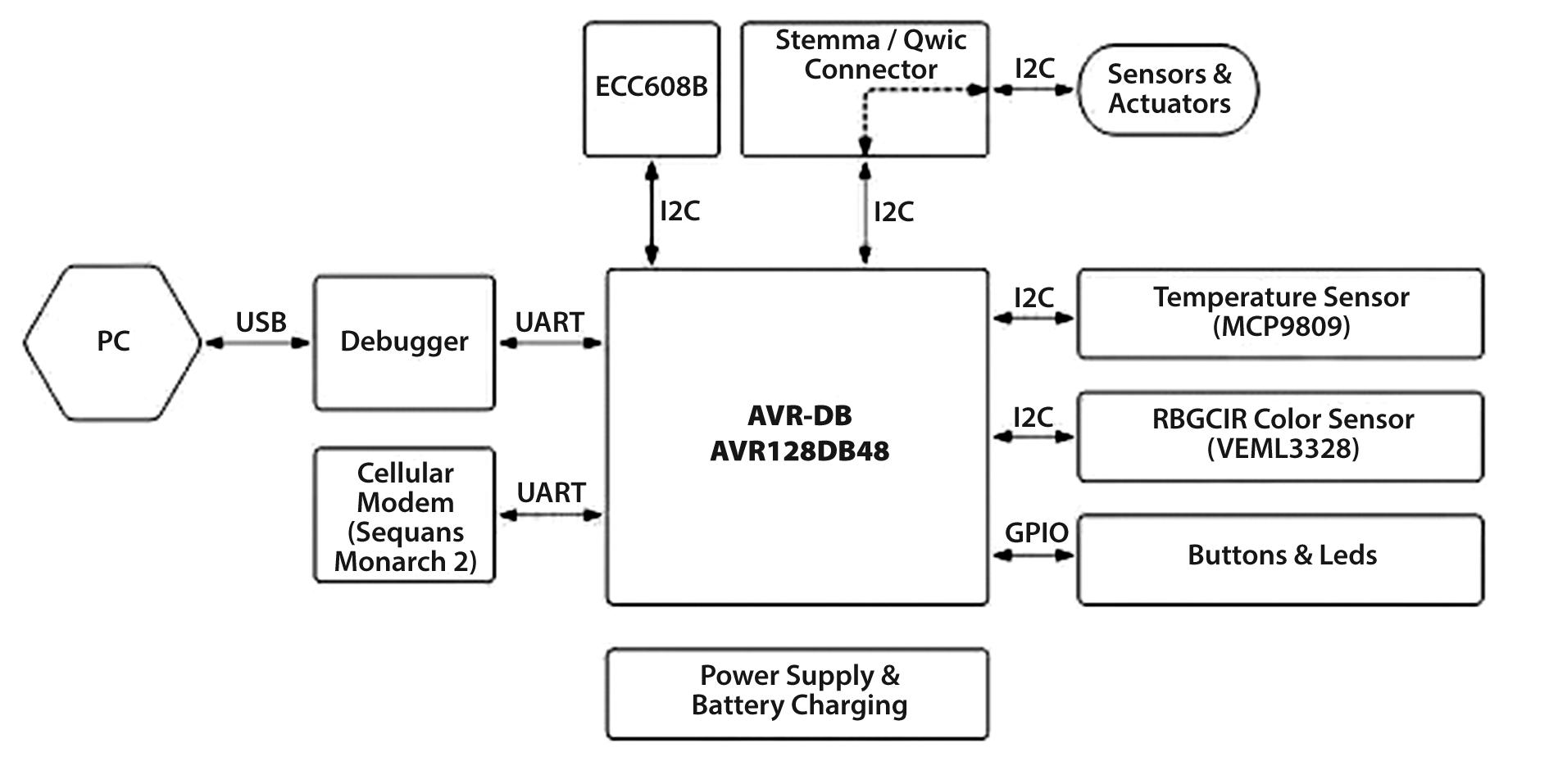
This AVR IoT development board block diagram shows that the connection to the host PC is via the debugger’s USB link, while programming of the application MCU is via the debugger’s UART link. Note the connection between the application MCU and the cellular modem is also via UART
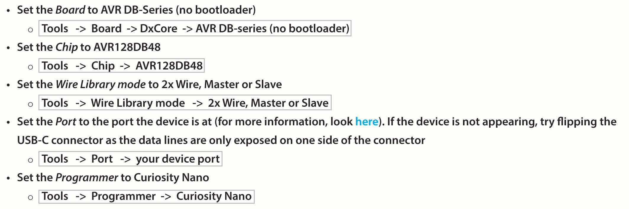
Getting started on application programming requires downloading and installing the Arduino IDE and DxCore. Next, the Arduino IDE needs to be configured to allow the AVR IoT cellular Arduino library to run (List 1).
These are also intended for current measurement purposes.
To measure power on the desired circuit, it is a case of cutting the strap and connecting an ammeter across the holes (Figure 5).
Once the IDE is configured the library can be installed. When this is done, several library examples for the development board can be accessed. Designers familiar with the Visual Studio Code IDE can use it for AVR IoT development, providing they install the Arduino plugin. Arduino application code developed in either IDE is ported to the development board’s MCU via the on-board debugger.
Cellular IoT is designed to run at low power to extend the life of battery-powered IoT end devices. It’s therefore important to optimize the application code toward minimal power consumption.
The development board also has a system voltage measurement circuit using its MIC94163 switch and a voltage divider connected to an ADC pin on the MCU, enabling on-demand measurement and preventing power leakage through the voltage divider. To measure the system voltage, follow these steps:
1 Configure the voltage reference for the ADC.
2. Set the MCU GPIO system voltage measurement enable pin (PB3) high to enable the voltage divider.
3. Set the MCU ADCO system voltage measurement pin (PE0) as the input for the ADC.
Conclusion
Cellular IoT is a popular LPWAN with increasing commercial potential. However, designing cellular IoT-powered end devices requires both hardware and software expertise. To enable designers, new cellular IoT development boards, such as Microchip’s EV70N78A AVR-IoT Cellular Mini Development Board, offer a quick prototyping route.
The development board uses a high-end LTE-M/NB-IoT modem and a popular Microchip MCU. Application code development is simplified using the Arduino or Visual Studio Code IDE.
■ Digi-Key Electronics www.digikey.com


Digi-Key recently launched new features to myLists, its platform that streamlines the ordering process for engineers, designers and their team members. These additions are part of the company’s commitment to better serving customers and supporting collaboration in the electronics industry. The new myLists features make the ordering process easier than ever for every stakeholder involved, no matter what stage a project is in. From shopping to quoting to ordering, the latest ability to easily share lists will improve the customer experience.
Before myLists, each step of the process was spread across different web services, making the experience cumbersome and time-consuming. It also had created challenges in timely ordering, which increased gaps in availability and frustration between collaborators.
Digi-Key’s recently released myLists feature streamlines communication and collaboration between engineering and purchasing. This vital line needs to be as seamless as possible to make sure that budgets stay on track and project schedules are met. myLists’ new list sharing feature solves this problem by making collaborating between engineering and purchasing as easy as a couple of clicks.
Digi-Key has added new customizable administrative privileges to allow users to be able to share their bill of materials (BOM) with anyone – internal partners or external team members – in just a few clicks. Anyone with the link will be able to view the shared list and if “editing” permissions are enabled, they will be able to edit the list as well.
This addition is key to expanding innovation in the electronics industry by empowering makers of any skill-level to share their lists, get feedback, order parts and communicate said list with any other team members who need insight into the BOM.


No one likes having to re-key information. It takes too much time, is frustrating and information can be lost due to human error. By being able to share BOMs, engineers, designers and procurement professionals are able to create their lists, compare the best options and convert it into quotes and orders without any data loss. It makes collaboration between engineers and the rest of their team easier and more seamless than ever by giving everyone the most up-to-date information and insight into how the project is progressing.


With a full suite of features that make quoting, ordering and managing a BOM a breeze, myLists is more powerful than ever. The full feature list for myLists includes:
• BOM Management – Share as much or as little as you want with team members with myLists’ customizable administrative permissions, read-only and edit. Be confident that the BOM is current and tracking availability from suppliers. With revision management, assembly controls and approved alternates, managing BOMs has never been so easy or error-free. Easily minimize gaps, reduce timelines and communicate with your team.
• Price and Availability – Each item has live pricing and live availability data, making it as easy as a click or two to add, approve or delete line items on your BOM.
• Quote Functions – Keep your budget stable despite the unknown future as well as up-to-date with myLists’ quote function where you can easily lock in pricing for 30 days and reference it anytime during the purchasing process.
• Assembly Controls – Without having to change the original quantities in your BOM, users can now multiply list quantities by a desired value. This streamlines when you need to move your BOM from a single product build to full production.
• List Preferences – Users can set and save preferences as a default for future lists, allowing for auto-updates to quantities or package type selections and notifications of price savings at higher quantities.

By uniting all of these capabilities in a single place, Digi-Key’s myLists ensures that engineers don’t lose their in-progress BOMs, can secure the best price, are able to get input from teammates and more easily manage the entire process to make sure everything stays within the desired timelines.

List builders can also easily make a copy of a list and add it to their own workflow, making this perfect for public collaborations or when you want to share the list without giving access to the original document. But when you do want to share the original, you can keep the administration privileges locked down so your collaborators get the latest updates in real time. No gaps and no missed communications. Only the most accurate information at your fingertips at all times.
Digi-Key’s myLists enable engineers, makers and designers across the globe to focus on innovation and collaboration with procurement teams while empowering purchasers to secure inventory faster. Digi-Key also believes that collaboration is central to innovation, which is why the latest features streamline every step of the purchasing process to bring people together to work on the parts of the process that matter most. By simplifying the sourcing process, every stakeholder, no matter if they’re an individual maker or a part of a large organization, can save financial resources, cut down on the time it takes to finish the project, and rest easy knowing that every person who needs to be involved has the insight they need, every step of the way.
The latest Wi-Fi standard, Wi-Fi 6, and its extension, Wi-Fi 6E, promise high data transmission speeds, higher capacity, and low latency, even in environments with many network subscribers. These advantages open up numerous new application options and areas of use, but also give rise to new requirements.
Author: Kerstin Naser Corporate Product Manager Wireless Rutronik

The much-cited refrigerator that automatically orders food has not caught on, but many other smart home devices have, such as washing machines that inform their owners via smartphone that the laundry is done. This is made possible by Wi-Fi, one of the best-known and most widespread wireless technologies. More and more devices offer a Wi-Fi interface, and not just in the smart home sector. Wi-Fi is also increasingly finding its way into industrial environments through applications such as mobile robots, crane systems, automated guided vehicles, or even safety and security systems and the networking of sensors in production lines. Virtual reality and gaming applica-
tions as well as wallboxes also use this wireless technology.
The new application areas also place new requirements on the technology; and despite the increasing number of subscribers in the Wi-Fi network, users expect a stable network connection. That is why the Wi-Fi Alliance is constantly further developing the standards. Since the first IEEE 802.11 protocol appeared back in 1997, data throughput has improved significantly with each new Wi-Fi standard. This time, however, the Wi-Fi Alliance has not only optimized the technology, but also the naming: Wi-Fi 6 and Wi-Fi 6E (E = enhanced/extended) replace the cumbersome title IEEE 802.11ax.
The predecessor standards have also been given new names: IEEE 802.11ac is now called Wi-Fi 5 and IEEE 802.11n is now Wi-Fi 4. Technically speaking, Wi-Fi 6 and Wi-Fi 6E offer a whole range of enhancements:

• OFDMA (orthogonal frequency division multiple access): OFDMA is an extension of the OFDM method used in Wi-Fi 5 technology. While only one data packet can be transmitted to a single terminal within a given time window when using OFDM, OFDMA enables the transmission of multiple sets of data for various terminals in the same data packet. This increases data rate efficiency and reduces network latency significantly.

• 1024-QAM (quadrature amplitude modulation): Compared to Wi-Fi 5, which uses the 256-QAM modulation method, 1024-QAM allows a 25% higher data throughput with Wi-Fi 6. With 1024-QAM, a total of 10 bits can be transmitted; with 256-QAM, it is only 8 bits. This is particularly advantageous in environments characterized by a high density of WLAN terminals, for example in railroad stations or at large events.
• MU-MIMO (multi-user - multiple input, multiple output): By breaking up the available bandwidth into separate spatial streams, communication via multiple antennas between an access point and multiple devices is possible simultaneously, both downlink and uplink. With Wi-Fi 5, this only worked for downlink. As a result, Wi-Fi 6 further reduces network latency and provides greater stability.
• TWT (target wake time): TWT “wakes up” network subscribers to transmit data only at specific times. The rest of the time, the devices “sleep” and thus require less energy. This also avoids interference in the network communication, since sleeping subscribers do not transmit data and do not block the communication streams – a decisive plus point, especially in industrial automation with many sensor applications.
• BSS (basic service set) coloring: Each BSS, consisting of an access point and the clients, is assigned a “color” (i.e. a number) as soon as another BSS is in its vicinity. Signals from another network can therefore be detected and ignored. This allows more efficient use of the streams and better transmission quality.
• Security standard WPA3 (Wi-Fi Protected Access 3): Compared to its predecessor standard WPA2, WPA3 provides significant enhancements in the area of authentication and encryption, as well as in the configuration of WLAN devices. Moreover, it ensures greater security at public hotspots. The WPA3 standard is mandatory for Wi-Fi 6 certified products.
Wi-Fi 6E offers even more advantages
Wi-Fi 6E offers more than just the previously mentioned advantages: extension to the 6 GHz band, for instance.
Wi-Fi 6E is also based on the IEEE 802.11ax Wi-Fi standard, thus supporting all the technologies mentioned, just like Wi-Fi 6. However, only the now heavily congested original 2.4 GHz and 5 GHz bands are defined for Wi-Fi 6.
In contrast, the 6 GHz band is also available with Wi-Fi 6E. Further 80 MHz and up to seven additional 160 MHz spatial streams for data transmission allow even higher data throughput with wider spatial streams. The 2.4 GHz and 5 GHz bands, which devices with older Wi-Fi standards use for transmission, are relieved, which in turn leads to lower latency. This makes Wi-Fi 6E an ideal solution for gaming, streaming, and virtual reality applications.
Switching over requires new hardware Anyone who is now considering switching to Wi-Fi 6 or Wi-Fi 6E should keep in mind that devices with older Wi-Fi standards cannot simply be upgraded to Wi-Fi 6/6E through a software update. This means that all routers and devices that need to use the latest standard must be equipped with new hardware. Wi-Fi 6/6E devices, on the other hand, are backwards compatible with older Wi-Fi standards.
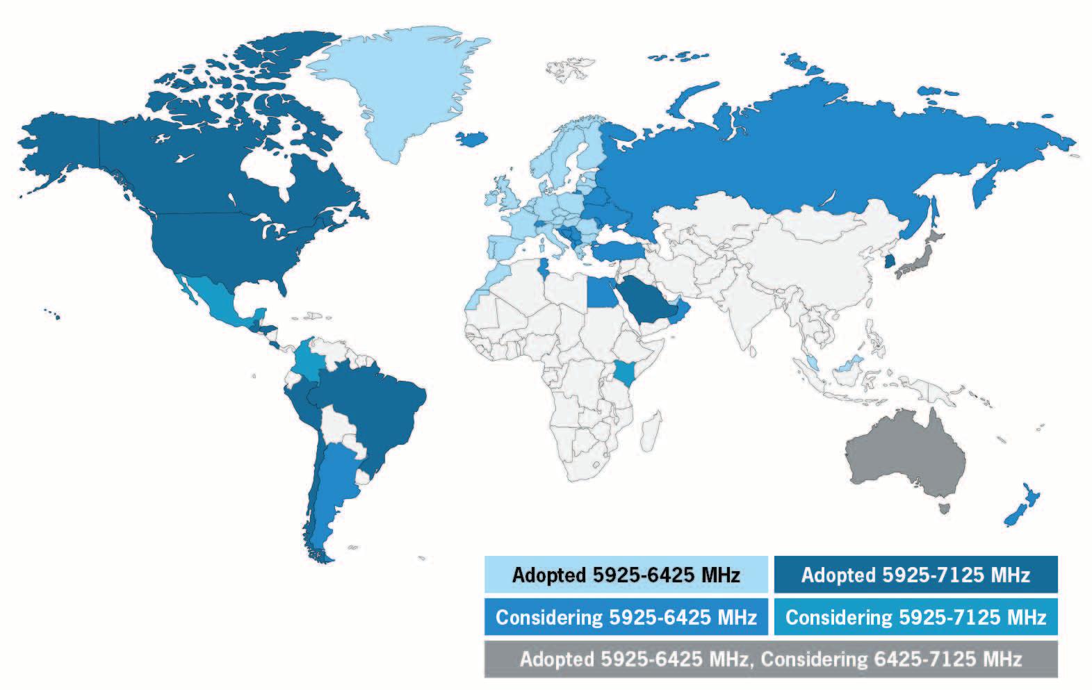
However, Wi-Fi use of the 6 GHz band has not yet been opened up in some countries. The USA started in 2020; Figure 1 shows which other countries have since followed its lead.
Rutronik already has products from various suppliers in its portfolio for both WiFi 6 and Wi-Fi 6E: Intel offers combination cards for Wi-Fi 6 and Bluetooth with its AX200 and AX201
models in form factors M.2 2230 and M.2 1216. Wi-Fi 6E cards are also already available with the two M.2 cards AX210 and AX211 from Intel. All Intel plug-in cards can be obtained in a range of variants, both with and without vPRO. AX210 is additionally offered for the industrial temperature range. Development kits are also available.
Silex offers a Wi-Fi 6 and Bluetooth 5.2 BR/EDR/LE card. SXPCEAX is based on Qualcomm’s QCA2066 SoC and is available in various form factors (SMT, half-size PCIe, M.2). The module is also certified for the 6 GHz band for Wi-Fi 6E.
Advantech has several Wi-Fi 6 plug-in cards in its product range: AIW-163 is an M.2 2230 card with an A-E Key (the key describes the connection form of the M.2 header) and a temperature range of 0 °C to 70 °C. AIW-165 in form factor M.2 2830 has an E Key and a temperature range of –40 °C to +85 °C. Advantech has announced two more M.2 2230 E Key cards for late 2022. Kits are also available from Advantech.
Module supplier Murata relies on chip sets from Infineon/Cypress and NXP for its Wi-Fi 6 and 6E products. Type 1XL is an NXP-based Wi-Fi 6 and BLE 5.2 2x2 MIMO module in a small form factor of 19.1 mm × 16.5 mm. More modules will be launched from the beginning of 2023: Type 2EA is based on the Cypress CYW55573 and will support Wi-Fi 6E. Type 2DL/2DR and 2EL/2ER are based on different NXP chips. The 2Ex variants also support Thread in addition to Bluetooth and Wi-Fi 6. The 2xR modules feature an extra antenna for Bluetooth.
Panasonic will also launch its first Wi-Fi 6 modules in 2023.
Rutronik offers complete routers with the new Wi-Fi 6/6E standard from Asus; and Silex also plans to add Wi-Fi 6E to its wireless bridges, device servers, and wireless presentation systems.

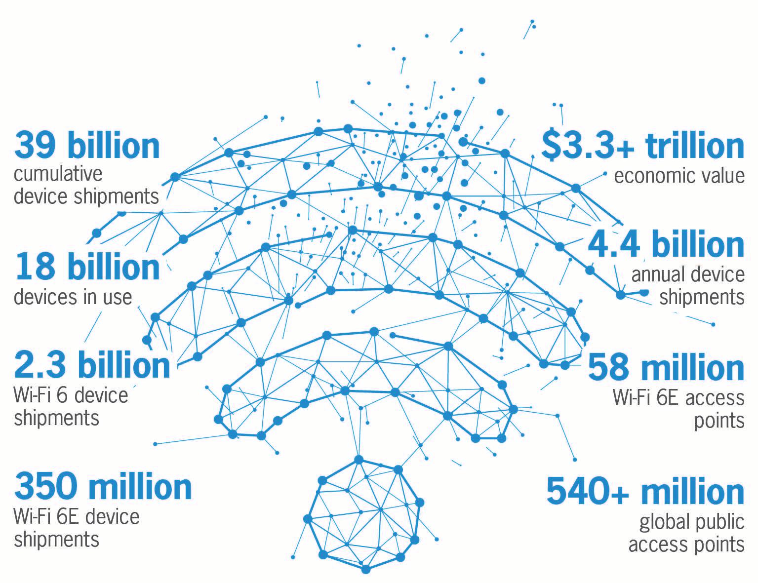
Established standard
Products are, therefore, available and numerous device suppliers are already applying them. According to information from the Wi-Fi Alliance, 2.3 billion and 350 million of the total 29 billion Wi-Fi devices shipped in 2022 will be equipped with Wi-Fi 6 and Wi-Fi 6E respectively (Fig. 2). Thanks to their advantages, the overall share of the new standards will certainly increase significantly.
While Wi-Fi 6 and Wi-Fi 6E are establishing themselves on the market, the Wi-Fi Alliance is already working on the next standard: Wi-Fi 7 or IEEE 802.11be. Users can look forward to three bands (2.4, 5, and 6 GHz) and even higher data transfer speeds. However, the Wi-Fi Alliance will not finalize this standard until mid-2024. So, it will be quite some time before hardware with Wi-Fi 7 is available on the market.
■ Rutronik www.rutronik.com
 Author:
This article presents a low power analogto-digital converter (ADC) solution for high precision measurement applications. A typical application in electrical engineering is the recording of physical quantities by sensors and forwarding of these quantities to a microcontroller for further processing. ADCs are needed to convert the analog sensor output signals into digital signals. In high precision applications, either SAR-ADCs or sigma-delta ADCs are used. With low power applications, every mW that can be saved counts.
Signal Conversion with Sigma-Delta ADCs
Sigma-delta ADCs offer a few advantages over SAR-ADCs. For one, they often have higher resolutions. In addition, they often come integrated with programmable gain amplifiers (PGAs) and general-purpose inputs/outputs (GPIOs). Thus, sigmadelta ADCs are well suited for DC and low frequency high precision signal conditioning and measurement applications. However, due to the high, fixed oversampling rate, a sigma-delta ADC often has a higher power consumption, which translates to a lower lifetime in the case of battery-operated applications.
If the input voltage is small - that is, in the millivolt range - it first has to be amplified so that it can be more easily managed by the ADC. A PGA analog front end (AFE) is required to connect a small voltage with a 10 mV output voltage. For example, to connect small voltages from a bridge circuit to a sigma-delta ADC with a 2.5 V input range, the PGA has to have a gain of 250. This, however, leads to additional noise at the ADC input because the noise voltage is also amplified.
The effective resolution of a 24-bit sigmadelta ADC is thereby drastically reduced down to 12-bit. However, in some circumstances, there is no requirement to use all codes in the ADC and at some point, further amplification no longer provides a dynamic range improvement. Another disadvantage of sigma-delta ADCs is the usually higher costs resulting from their internal complexity.
Benefits of Combining a SAR-ADC with an In-Amp
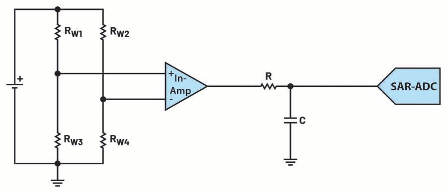
The function of a SAR-ADC can be divided into two phases: the data acquisition phase and the conversion phase. Basically, in the data acquisition phase, the current consumption is low. Most SAR-ADCs even power down between conversions.
In contrast to such slow measurements, sigma-delta ADCs have the strengths of oversampling, while using a much higher internal oscillator frequency than the output rate. This allows designers to optimize sampling for higher speeds with worse noise performance or for lower speeds with more filtering, noise shaping (pushing the noise into the frequency band outside the area of measurement interest), and better noise performance.
However, that means a lot more power consumption with sigma-delta ADCs compared to SAR-ADCs. The effective resolution and noise-free resolution of many sigma-delta ADCs are mentioned in their data sheets, making it easy to compare the trade-offs.
Conclusion
Both sigma-delta ADCs in combination with PGAs and SAR-ADCs with an in-amp are suitable for signal conversion in high precision measurement applications. The solutions both have a similar accuracy.
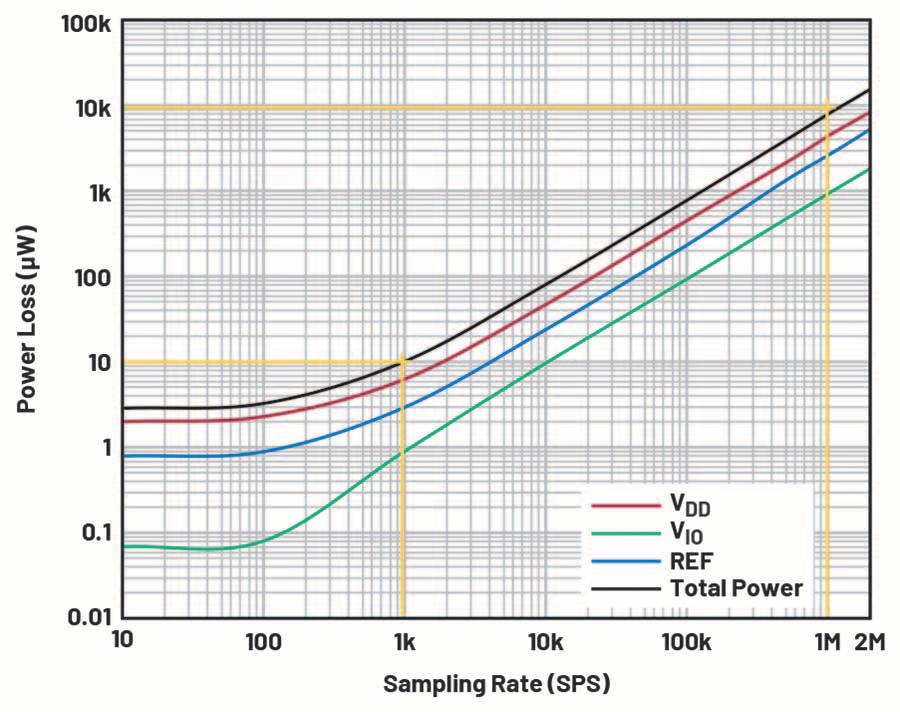
So, the conversion phase draws the most current. The power consumption is dependent on the conversion rate and linearly scales with the sample rate. For power-saving applications for slowresponse measurements - that is, measurements in which the measured quantities change slowly (for example, temperature measurements) - a low conversion rate should be used to keep the current draw and thus the losses low.
Figure 2 shows the power losses in the AD4003 at various sampling rates as an example. At 1 kSPS, the power loss is approximately 10 μW; at 1 MSPS, it has already risen to 10 mW.
For power-saving or battery-operated measurement applications, however, the combination of the SAR-ADC and the inamp is better because it offers a lower power consumption and lower costs compared with the solution consisting of the PGA and the sigma-delta ADC. In addition, a PGA with a high gain often limits the performance because the noise is also amplified. This article just covers one possible solution for a SAR-ADC.
There are more integrated solutions available such as a sigma-delta converter like the AD7124-4 / AD7124-8 with an integrated PGA. ■

On 11th of February 2020, the International Committee on Taxonomy of Viruses adopted the official name ‘severe acute respiratory syndrome coronavirus 2’ for the coronavirus that causes COVID-19 otherwise known as SARS-CoV-2. During the past two years or so, in one way or another the world population has been affected by this virus, and the polymerase chain reaction (PCR) test has entered into our daily lives. At this point we could quite easily question what a power supply has to do with PCR, but behind the scenes the power supply industry and the latest digital power technologies have contributed greatly to make the PCR process efficient and accurate. Before we disclose how, let’s go back in time to the origin of everything.
Author: Patrick Le Fèvre Chief Marketing and Communication Officer Powerbox (PRBX)

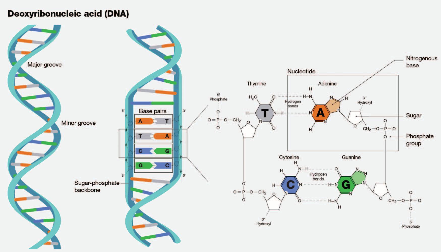
Reading inside the double helix! We all learned at school about the human hereditary material known as deoxyribonucleic acid, or DNA, carrying all the genetic information and instructions needed for organisms to develop, grow, survive, and reproduce. Originally discovered in 1866 by Gregor Mendel, known as the ‘Father of Genetics’, it was to be many years later that scientists discovered how to break the DNA’s secret code and how it could be best used for the good of humanity.
With high regard for the numbers of scientists making discoveries, a major cornerstone was reached in 1953 when James Dewey Watson and Francis Harry Compton Crick published on DNA’s double helix structure that twists to form the typical ladder-like structure we have all seen in many repre-
sentative forms (Figure 1). Their work was rewarded in 1962 with the Nobel Prize in Medicine, which they shared with Maurice Hugh Frederick Wilkins for their discoveries concerning the molecular structure of nucleic acids and its significance in information transfer in living material. DNA composition is like individual letters of the alphabet. When they are combined with one another in a specific order they form to make words, sentences, and stories. Reading the book and understanding its contents required intensive research and it was only in March 2022 that scientists finally mapped the first complete human genome, composed of more than 3 billion of base-pairs. It is hard to visualize what it represents, but translated into something more tangible it would be the equivalent of a book with one million
pages – a lot of bed time reading. The completion of the human genome has been made possible by a great number of technological innovations e.g., Oxford Nanopore’s DNA sequencing method which can sequence up to 1 million DNA letters at once but with some mistakes, and the PacBio HiFi DNA sequencing method, which can read 20,000 letters with 99.9% accuracy. Great achievements, but both would not have been possible without pioneering inventors’ discoveries.
Understanding DNA has been a very important research area and a developing toolbox to decode, it is the dream of every biochemist and it is worth mentioning Kary Banks Mullis who in 1983 invented the PCR that has contributed to boost the research and speed of in depth DNA understanding.


The DNA copy-machine is born! Urban legend or reality? it is said that in 1983 while driving from the Bay area to his cabin in Mendocino, like a bolt of lightning out of the California sky Dr. Kary Banks Mullis imagined a way to pinpoint a particular stretch of DNA and synthesize an enormous amount of copies. At that time Mullis worked for the company Cetus and focused on turning his vision into a process. After many ups and downs, in 1987 Mullis submitted a paper to the review Nature: “Methods in Enzymology” which was the trigger of the PCR evolution. In 1993 he received a Nobel Prize in chemistry for his invention of the polymerase chain reaction (PCR). The process, which Mullis conceptualized in 1983, is hailed as one of the monumental scientific techniques of the twentieth century.
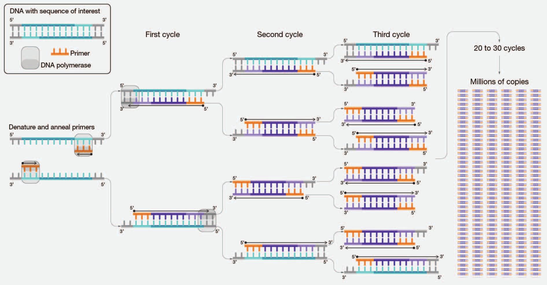
The polymerase chain reaction (abbreviated PCR) is a laboratory technique for rapidly producing (amplifying) millions to billions of copies of a specific segment of DNA, which can then be studied in greater detail. PCR involves using short synthetic DNA fragments called primers to select a segment of the genome to be amplified, and then multiple rounds of DNA synthesis to amplify that segment (Figure 2). This is done by using a specific process that requires the samples to be placed in tubes and exposed to a very
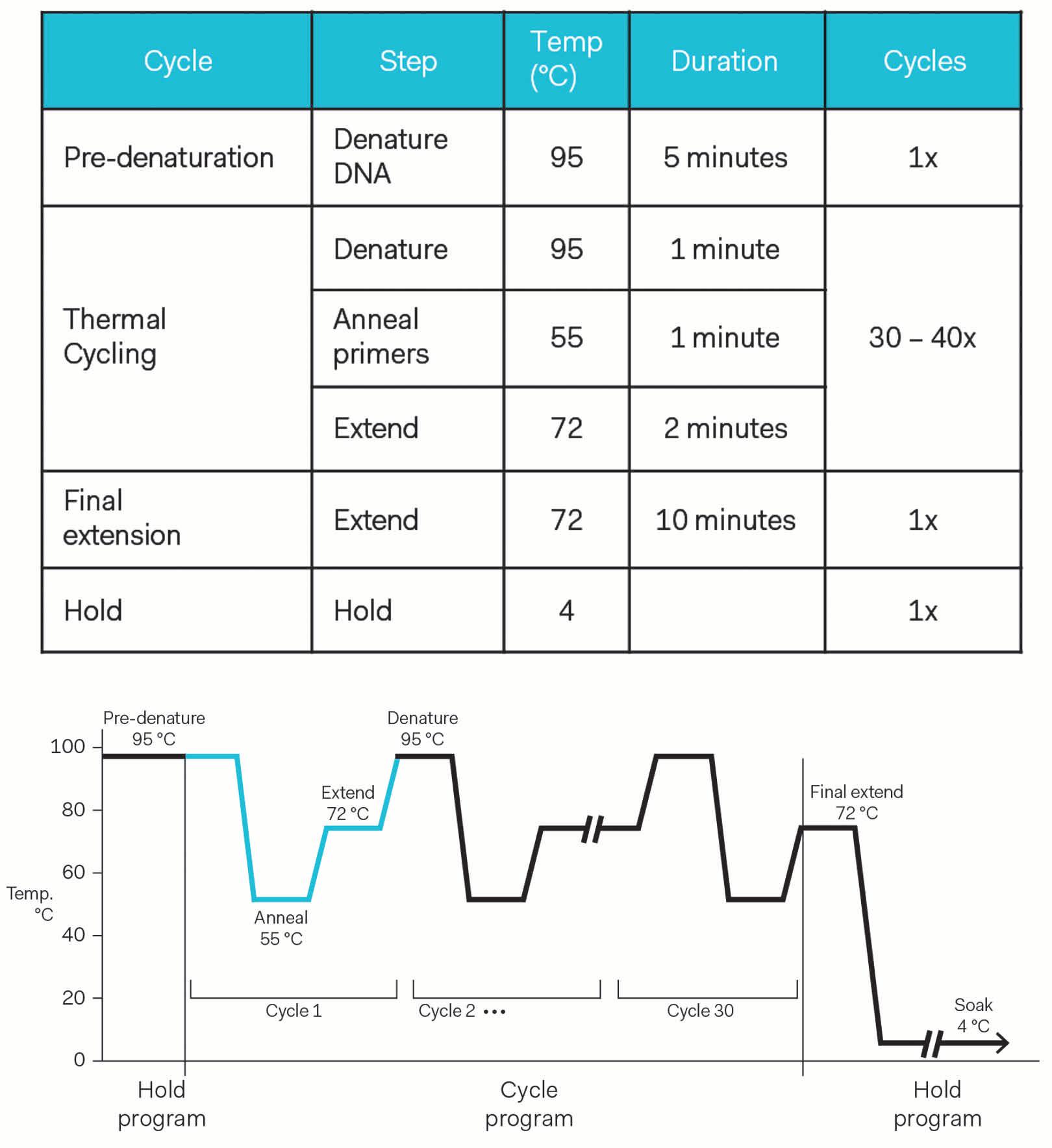
precise thermo-cycling, and this is where the power supply meets the DNA! This process includes several steps but three are the most critical (Denaturation, Annealing, Extension) and repeated a number of times to make copies of the DNA segments (Figure 3). Without entering into too much detail we can summarize the three critical steps below:
The preparation contained in the tube is heated to at least 94°C. The heat breaks the hydrogen bonds of the original DNA sample and separates the DNA into single strands.
The temperature is lowered to approximately 5 °C below the melting temperature of the primers, between 50 to 60°C, allowing the DNA primers and the DNA polymerase enzyme to bind to the individual strands of DNA that were separated by the heat. At this point, the nucleotides (A, T, C, G) from the added mixture solution will pair with the individual separated strands of DNA that resulted from the heating process.
The temperature is then increased up to 72°C to start the extension process. Then, once segments are joined together they form a new complementary strand of DNA.
A new duplicate double-stranded DNA molecule has been formed from each of the single strands of the original sample molecule. When the sequence is completed the temperature is then increased to start a new cycle. Steps one to three are then repeated about 30 to 40 times which automatically repeats the heating and cooling cycles of the process, resulting in the DNA sequence being doubled each time the heating/cooling cycle is conducted. At the end of the process millions of copies of the original sample are obtained.
A final step of extension is required to allow all the PCR products to be correctly synthesized, usually at 72°C for 10 min. Finally, the temperature should be reduced to 4°C to store the PCR product until analysis.
Depending on the final target, time or level of accuracy required, variations of this process are often used e.g., Quantitative real-time PCR (qPCR), Reverse transcription-PCR (RT-PCR), Reverse transcriptionquantitative PCR (RT-qPCR), Digital PCR (dPRC) and digital droplet PCR (ddPCR), Microfluid PCR.
There are many medical applications requiring thermal control e.g., neonatal incubators, blood warming for Hemolysis, laboratory incubation chambers and so on.
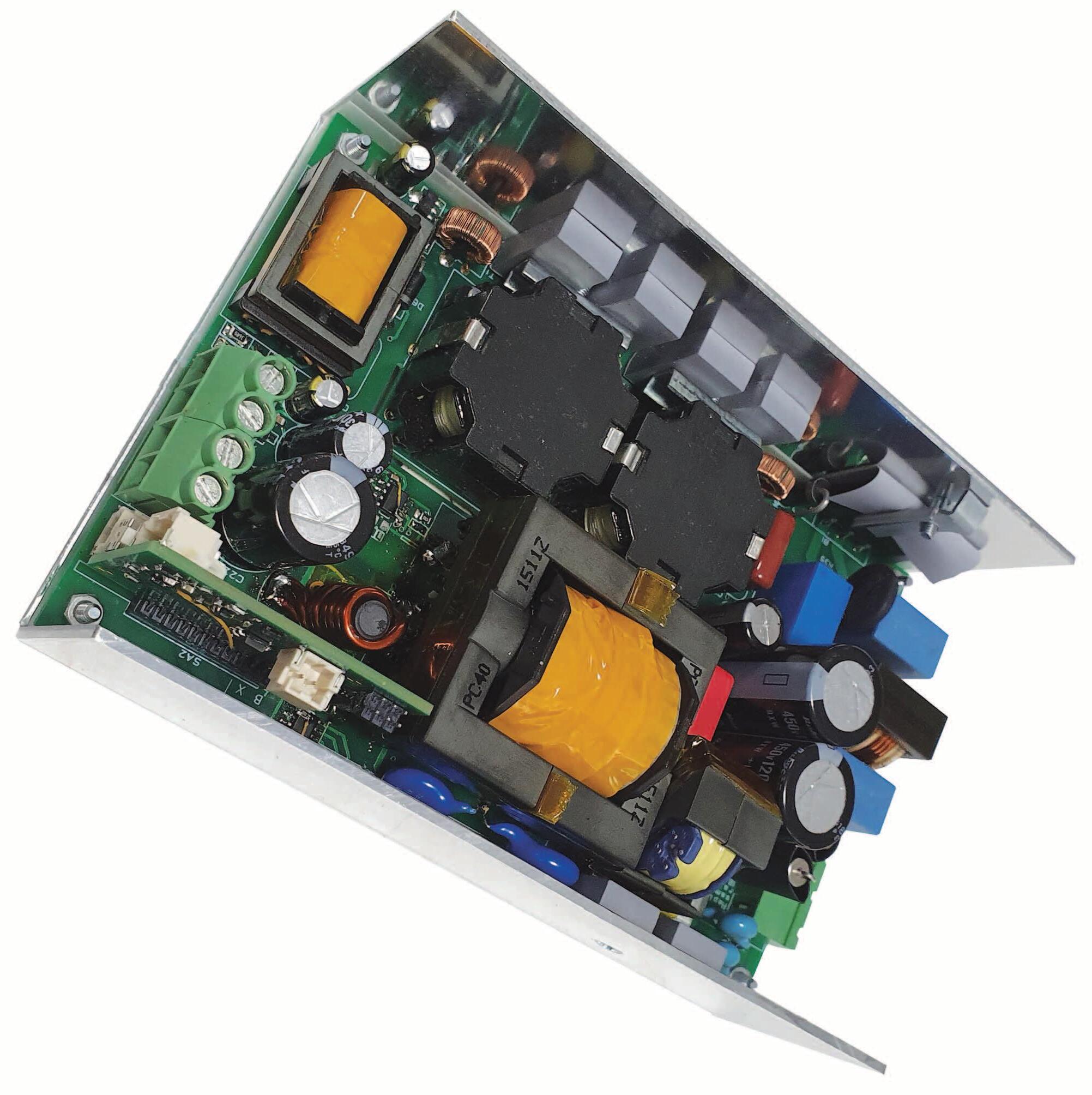
Most of those applications require accurate thermal regulation and most of the medical power supplies with output voltage control are suitable for such applications. In the case of the PCR equipment
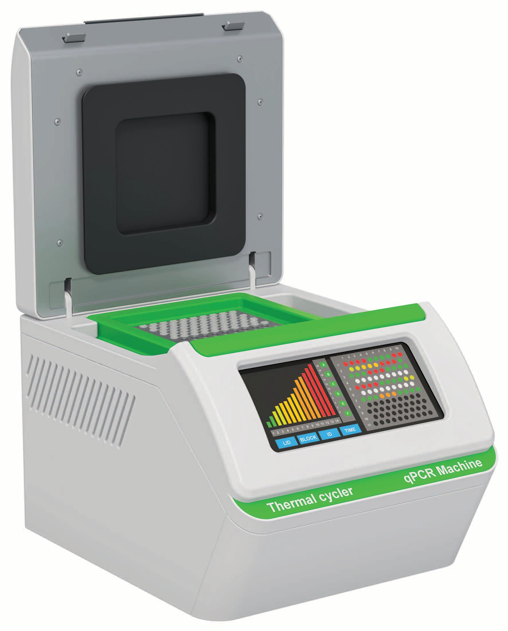
(Figure 4) and the specificity of the thermal cycling with high accuracy and repetitive sequences, they require a specific power solution, and often adopt a modular approach with the power train and control
built in the PCR thermal-control loop. As shown in figure 3 the thermal cycles are fairly short, requiring the heating element to adjust its temperature between +95C high, +50C low, +72C plateau and back to +95C after four minutes. This cycle is repeated 30 to 40 times, with a very high accuracy level. There are different methods to generate and control the temperature in thermocyclers but many are using Peltier effect elements. If the main application of the Peltier effect is cooling, the Peltier effect can also be used for heating or control of temperature. It could also be associated to another heating element and then using a controlled hysteresis, cool down the thermal chamber. PCR thermocycler manufacturers have developed very
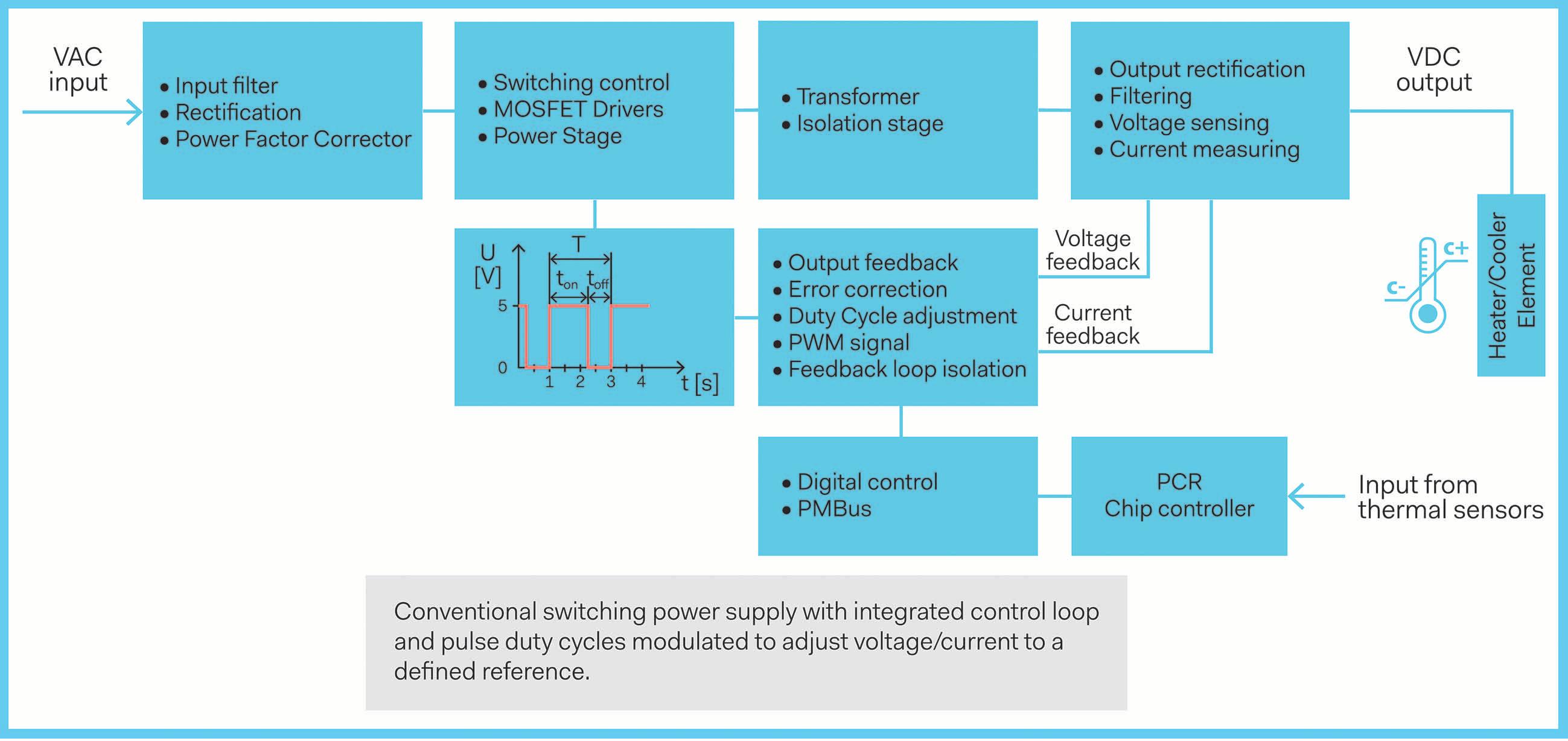
Power supply controlled by and external PWM signal part of the PCR control loop.
complex algorithms to adjust and control the level of temperature with high accuracy. With the introduction of digital power and control and energy management it has become easier to interface the thermocycler CPU to the switching stage and to control voltage and current via a digital interface e.g., PMBus, to power the heating/cooling elements (Figure 5).
In some case the PWM signal is generated by the thermocycler controller and injected into the power supply switching stage to tightly control the parameters without additional steps (Figure 6).
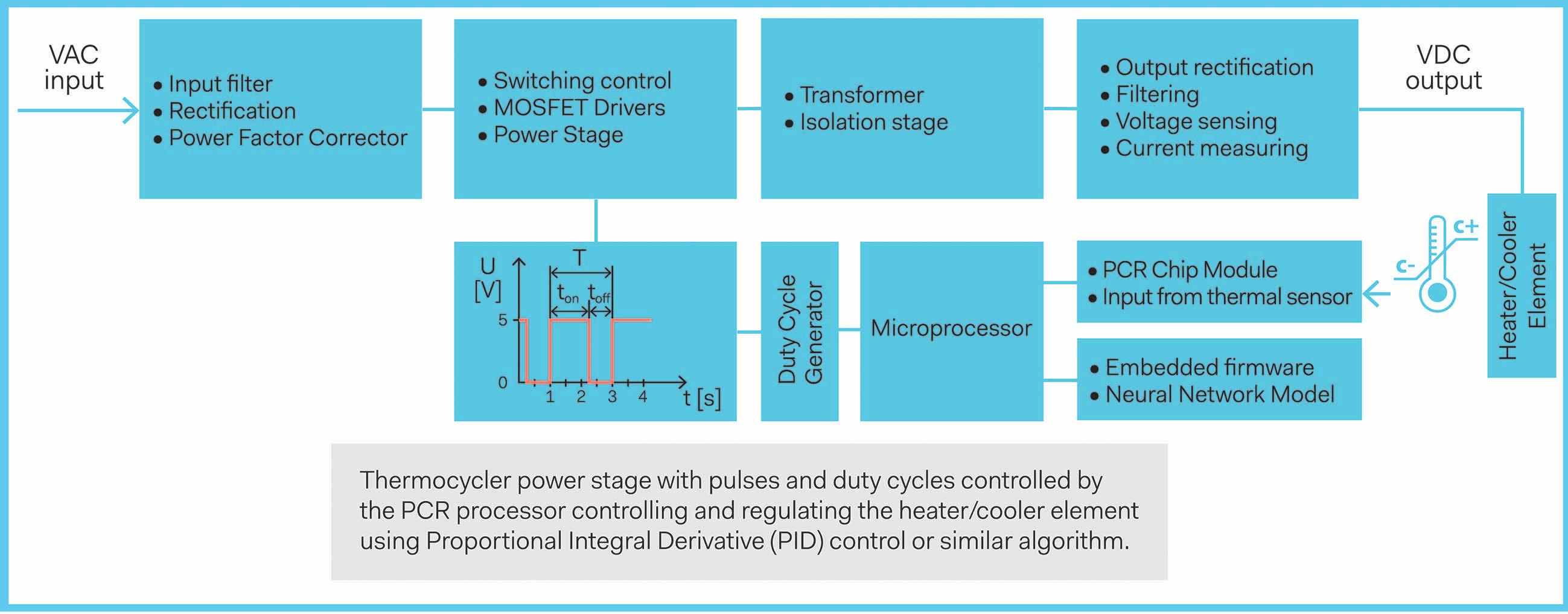
Because the power stage is highly integrated into the thermal control loop, it often becomes a part of it and power designers have to work in close cooperation with the programmers to offer the
most optimized response time to a spe cific demand, which is very interesting and indeed quite different from the more conventional ways of working when designing power solutions.
From its discovery by Dr. Kary Banks Mullis in 1983 to the mass application to detect the presence of SARS-CoV-2 virus in billions of samples, PCR technology has played a very important role in med ical research and public health. This has also been a very interesting area for power electronics engineers to design power solutions (Figure 7) in tight coop eration with the medical industry to develop very specific power supplies with a high level of programming and system integration. Who said the power supply industry is boring?
https://www.science.org/doi/10.1126/science.abj6987
https://www.genome.gov
■ PowerBox www.prbx.com
In this article, we will discuss an easy and cost-effective way to accurately measure your product’s temperature while also deploying unique bestin-class safety and reliability functionality in your system, would you be interested in learning more.
First, integrated NVM use provides the capability to record critical data locally in the temperature sensor. An example of critical data is logging temperature extremes of the end-product that could force system shutdowns or failures, record temperatures, date/time, fault counts, power-on duration and many other things designers would like to avoid.
Consider the impact to your future product improvements if you could review and study your end customer product failure returns by simply reading the integrated memory inside the temperature sensor. You could learn things like how many times the product reached a critical temperature and the date and time it occurred.
This data alone could tell you if your customer operated the product in a consistently harsh temperature environment, perhaps voiding the warranty or any warranty claims due to customer misuse. The integrated memory could be viewed almost like the crash data recorders found in cars and planes today.
The stored data could help improve future product development and or product improvements by relating the stored temperature violations to, perhaps a wrong component selection where its performance degraded over time.
Second, the integrated memory enables the capability to track how your end customers are using your product’s features or functions to determine if customers actually use them or not. Perhaps you have new features or specific new functions that you want to try out with customers.
Today’s electronic systems are running faster, but their silicon content continues to increase as well. That means applications are generating more heat than ever before, making real-time temperature monitoring vital to the operation of industrial, consumer, computing, and communications designs.
Increasing your product’s operational value to your customers, while protecting your investment, is critical to long term success. This is only available with Microchip’s integrated (Non-volatile Memory) NVM temperature sensor family. You might be wondering why it is important to use the integrated NMV inside; we will share three important reasons.
This new access to data will allow you do get important information about what your customers are using in your designs. These results could be even more valuable than a customer survey or even a focus group!
The final reason to use integrated NVM is for critical data storage for factory, system configuration settings and parametric data. The integrated memory could be used to store critical factory testing information about how the product was tested to certain test program revision. The test setup and equipment location, along with its parametric data, would help on customer product returns by providing unbiased information on how the product was factory tested. In addition, the integrated memory could be used to store critical system configuration data that helps the power up and initialization process to configure the system or product. The value here is that future product upgrades could be done by simply reprogramming the previous configuration data in one simple programming operation.
The AT30TSE752A/754A/758A contain the world’s only set of nonvolatile registers to retain the configuration and temperature limit settings even after the device has been power cycled, thereby eliminating the need for the device to be reconfigured after each power-up operation. This additional flexibility permits the device to run self-contained and not rely upon a host controller for device configuration. In addition, these devices contain a full array write protection feature via the Reversible Software Write Protect (RSWP) mode that once enabled, disables the EEPROM write circuitry and therefore, protects the contents of the entire memory array against any intentional or unintentional write operations.
A temperature sensor with integrated EEPROM, such as the AT30TSE758A from Microchip, enables manufacturers to take advantage of the three core benefits discussed above. Precise temperature monitoring devices combine a high-precision digital temperature sensor, programmable high and low temperature alarms,
integrated nonvolatile registers and 8 Kbit EEPROM into a single compact package. These features make it applicable for use in a wide variety of applications like consumer, industrial and computing that require measurement of local temperatures as an integral part of the system’s function and reliability.
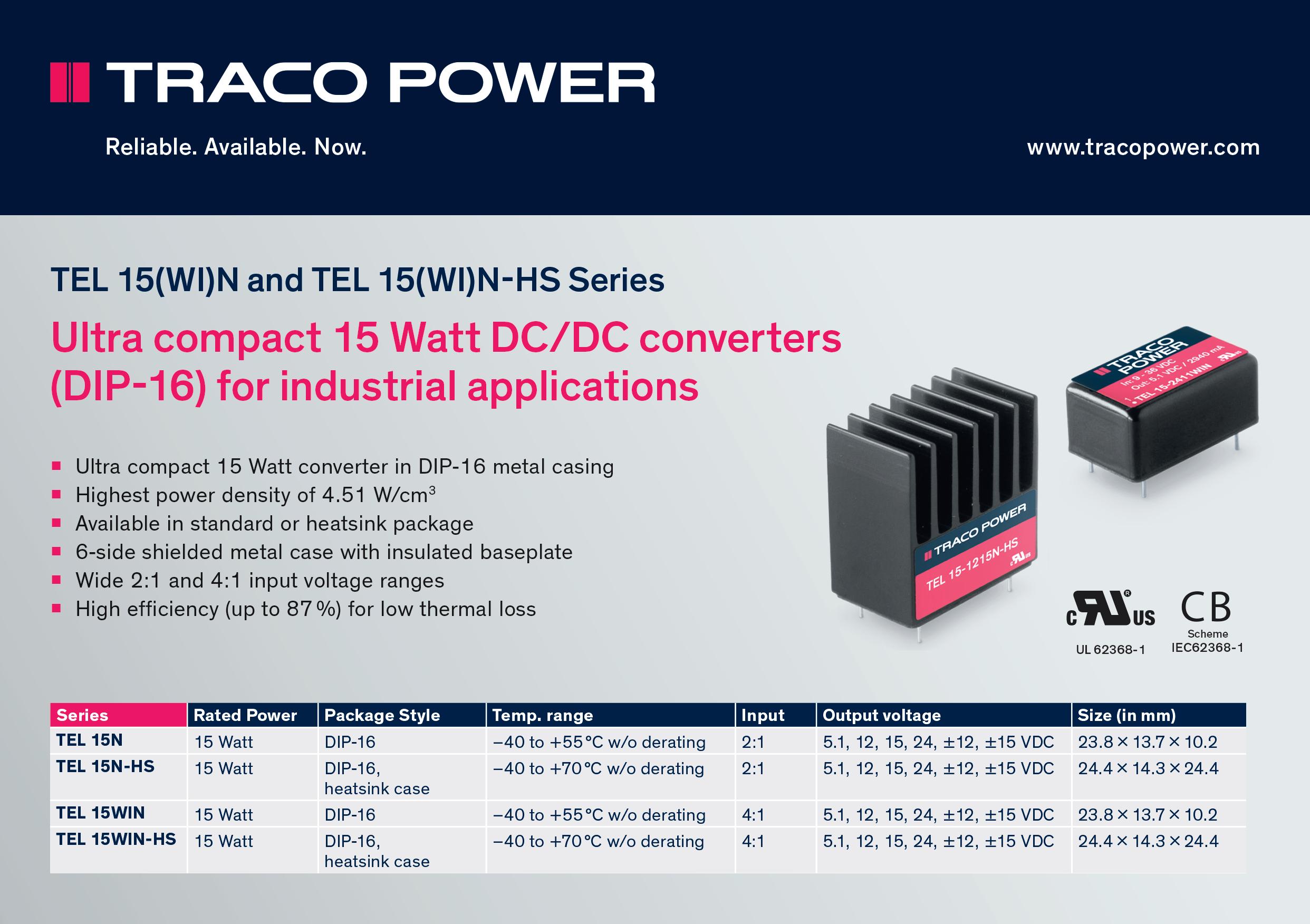
Conclusion
Using integrated NVMs that complement your thermal management endeavors is extremely important, and we hope this article has helped explain why. Microchip is committed to this market segment, which is why we’ve created the AT30TSE752A/4A/8A product line, which allows designers to bypass the typical thermal design roadblocks, improving the safety and reliability of an application. For more information, please visit https://www.microchip.com/wwwproducts/en/AT30TSE758A
■ Microchip Technology www.microchip.com
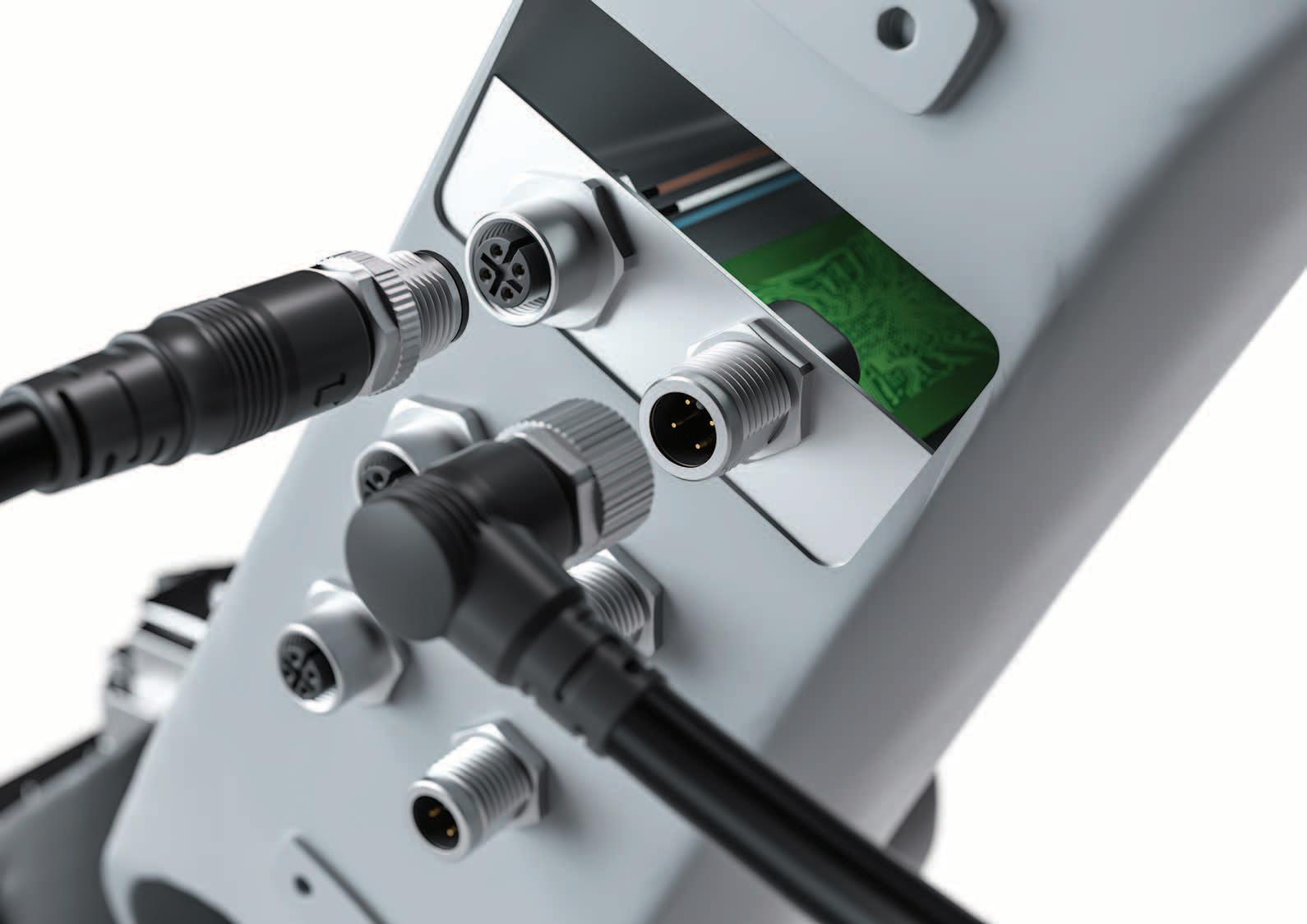
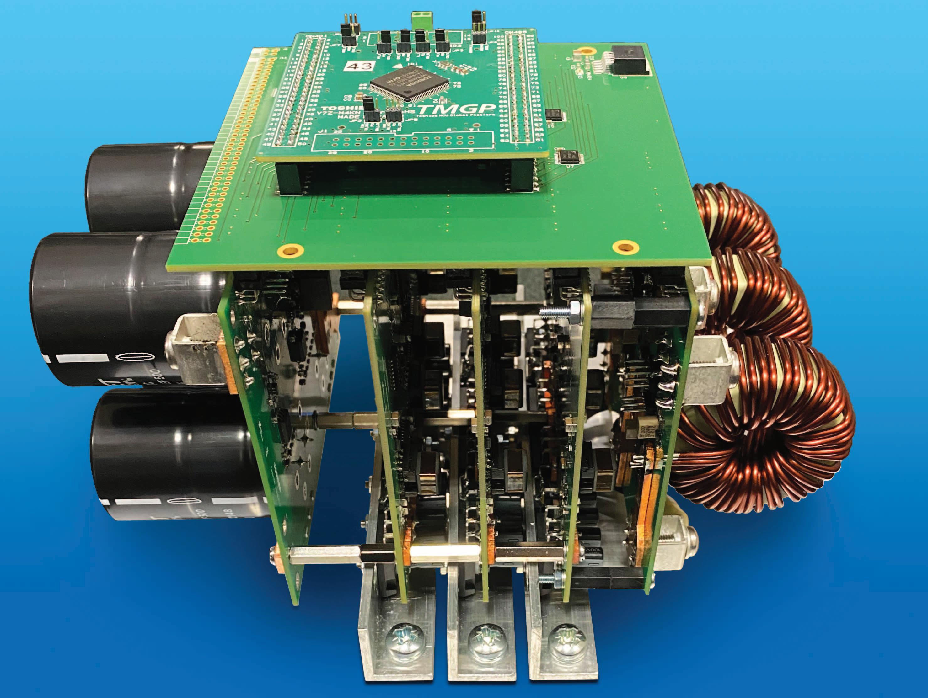
Würth Elektronik now offers a wide product portfolio of A-coded M12 circular connectors (DIN EN 61076-2-101). The high-quality female and male connectors with screw mating for panel mounting and cable attachment are suitable for use in harsh environments with moisture, dust and vibration. WR-CIRCM12 is available in four-, five- or eight-pole versions.
M12-A stands for data cables with the option of DC power supply – particularly suitable for fieldbus applications in industry, manufacturing engineering and automation. Sensors and actuators can be connected via the robust dustproof and waterproof connections with IP67 or IP68 ingress protection. Packaging variants are available with metal or plastic bushings. The O-rings and seals are made of elastomers and epoxy resin and the contacts are gold-plated. All solderable products from the WR-CIRCM12 family have UL94V0 certified packages, and the pre-attached cables and field-attachable products with screw terminals comply with UL94-HB. The M12-A product group includes cables with male or female connectors, field-attachable connectors as well as plugs and receptacles for device installation, including prewired connectors or those to be placed on the board as THT components, for example. Free samples can now be ordered.
■ Würth Elektronik eiSos
www.we-online.com
Toshiba Electronics Europe GmbH (“Toshiba”) is fully prepared for this year’s PCIM conference and exhibition (Nuremberg 9th – 11th May). The company will use the event to showcase its latest engineering advances in making industrial and automotive power systems more efficient. These will underline the instrumental role it will play in society’s progression towards carbon neutrality. Developed at the High Voltage Lab that Toshiba has established in Dusseldorf, the intention of the SiC-CUBE proof-of-concept is to accelerate power system implementation by leveraging parallelism. This totem-pole power factor correction (PFC) building block supports 22kW 3-phase operation. It is based on the company’s latest wide bandgap technology – featuring its third generation SiC MOSFETs, as well as Schottky barrier diodes and smart gate drivers. By having such closely matched constituent components, it has been possible to deliver a fully optimized PFC reference design platform on which highly effective power systems can be developed. Its power switching boards, plus inductor and capacitor boards, are all connected to a TMPM4K microcontroller board via individual bridge legs. The 3D stacking arrangement means major footprint savings are realized.
Achieving industry-leading power density, the SiC-CUBE has a compact 140mm × 140mm × 210mm form factor (which is then attached to a heatsink). Use of 650V-rated MOSFETs, rather than ones with 1200V ratings, presents a more cost-effective modular way of implementing PFC than competing solutions, with system bill-of-materials costs kept down. Thanks to the 3-level configuration, the voltage swing across each MOSFET can be restricted, so the power losses experienced are minimized. The coupling of DC-DC converter hardware to the PFC will result in creation of off-board EV charging infrastructure, while the addition of inverter hardware will address renewable energy generation requirements.
Among the highlights of the Toshiba booth at will be the SiC-Cube proof-ofconcept developed at the Duesseldorf Toshiba High-Voltage Lab. It supports the acceleration of power system design and their implementation. Alongside SiC-CUBE, there will be a multi-axis robot arm demonstration. This will also rely on one of Toshiba’s TMPM4K motor control MCUs (and accompanying software) for smooth, high-precision FOC-based movement, with 3 motors being driven simultaneously. It also utilizes cutting-edge MOSFET, photocoupler and voltage regulator technology.
■ Toshiba Electronics Europe https://toshiba.semicon-storage.com/eu/top.html

The success of a product also depends on the efficient development of the embedded software. For this, developers and teams must be able to work together as flexibly as is optimal for them. The central question is, what features and capabilities do development tools need to bring to make this possible?
Authors: Ralf Kern, Line Manager, Rutronik Clark Jarvis, Senior Staff Technical Marketer, InfineonMost semiconductor manufacturers offer their own development tools to support efficient product development for their components. Whether these provide everything necessary for this can only be answered if more is considered than just the pure tools. Rather, a holistic development environment consisting of hardware and software tools, embedded runtime drivers, libraries, documentation and more is needed.
Using Infineon's ModusToolbox™ software as an example, we will show here what actually increases the efficiency of the embedded engineer's development work.
ModusToolbox software is an extensible development environment that supports a wide range of Infineon microcontrollers and development kits. It includes a collection of various development tools, libraries and embedded runtime assets for flexible embedded software development.
The desktop applications can be used to create new embedded projects, manage software components and configure device peripherals and middleware. Add to that the typical development tools for compiling, programming and debugging.
They leverage numerous GitHub-hosted repositories from Infineon and partners that include code samples, board support packages, middleware and application support. Together with documentation, training content and a support community, the result is a complete workflow for embedded developers.
If you set out to find the ideal workflow for embedded systems development, you do not have to look far. The first engineer you ask will swear that the workflow they personally follow is the right one.

Therefore, since each development team or embedded developer has an own unique workflow, the development environment should provide a high degree of flexibility. This is also a central pillar of ModusToolbox software.
The heart of the development process is the integrated development environment (IDE). The embedded developer on a daily basis when coding and debugging embedded firmware uses it. Ideally, it should be a familiar environment for every developer. ModusToolbox includes an Eclipse-based IDE for users who want to develop within the Eclipse framework and with the Arm® GCC compiler. As an alternative editor, Microsoft VS Code is available, which uses exactly the same Arm GCC toolchain and build commands. Through the VS Code extensions, it provides full programming and debugging capabilities.
In addition, ModusToolbox projects can also be used on all leading IDEs and toolchains with native support for IAR Embedded Workbench and Arm Microcontroller Developers Kit (μVision). However, a flexible and efficient development environment must go beyond visual code editors and graphical debugging. That is why the core of ModusToolbox software is a Makefile-based build system and a command-line shell to automate build systems and facilitate a continuous integration workflow. This scriptable build system is crucial for a truly flexible development environment that can be tailored to the exact requirements of the developer While doing so, he can be sure that the compiled output will be consistent with the supplied Eclipse IDE or VS code because it uses exactly the same build system commands and compiler options.
Such support for scriptable build commands and continuous integration lead quasi-automatically to workflows for collaborative development. Version control, Git repositories, make recipes - they are critical to the way embedded runtime assets are distributed and managed within ModusToolbox. At the same time, they are the central components for collaborative development within a team.
Extending these capabilities of Modus Toolbox to the user application code allows developers to collaborate efficiently
within the team and ensure the correct versioning of the provided drivers, middleware, libraries and BSPs consistently in the continuous integration build flows.
the underlying hardware specifics are hidden in favor of typical use case functions. It also enables rapid integration of middleware libraries and communication stacks.
HAL and low-level drivers open up more possibilities
For embedded engineers, every decision represents a balancing of tradeoffs and optimizations. From the choice of device and product features, to the ideal balance between their performance and capabilities on the one hand, and cost and power consumption on the other, to the specific APIs used to develop an application.
Often the possibilities for optimizing the APIs are limited by the drivers provided by the semiconductor manufacturer. Not so with the ModusToolbox software. This is because it provides both low-level peripheral drivers and a hardware abstraction layer (HAL). The hardware abstraction layer provides unified APIs that are consistent across different device families. As a result, application code developed with these functions is highly reusable and typically easier to program because some of
However, compromises have to be made when working exclusively on an abstract level. This is because any kind of abstraction leads to a certain degree of inefficiency, and the further you move away from the underlying hardware, the more you move away from the detailed control of the peripheral in question. In contrast, lowlevel drivers give full control over the peripheral. They also provide functions specifically designed for the features and capabilities of the corresponding device.
Since ModusToolbox offers HAL and lowlevel drivers, an embedded developer can use both within one application. On the one hand, this makes it possible to achieve the necessary balance between portability and code reuse with HAL APIs, but on the other hand, it also makes it possible to develop code in such a way that is tightly coupled to the capabilities of the hardware.
From this point of view, code and memory-saving software can be developed that is optimally adapted to the specific application in question.
Middleware and libraries
Another challenge for embedded engineers is the integration of libraries and middleware. Most semiconductor vendors provide access to an industry-standard ecosystem of middleware that is specifically developed and provided by that vendor, sometimes in collaboration with partners.
In some cases, however, the offering is very rudimentary. Others provide reference examples within the development environment. These can act as a starting point and show that the middleware can work on the hardware in question. Modus Toolbox also has code samples within the ModusToolbox Project Creator for sample projects from Infineon and partners.
The embedded developer is often left with the task of integrating this middleware into his specific application.
ModusToolbox makes this possible with a library manager that is able to collect the necessary source files from Git Hub repositories, resolve any dependencies on related middleware, and update the necessary make recipes to include the selected sources. The documentation provided with each middleware source folder describes in detail all Makefile changes necessary to use the middleware in the application.
The foundation for efficient development is a flexible development environment that allows embedded developers to define their individual workflow. Together with one of the supported PSoC™ microcontroller development kits, ModusToolbox provides this kind of flexibility, from the choice of supported IDE or command line build support to the various options for driver APIs and middleware integration.
■ Rutronik www.rutronik.com


Renesas Electronics Corporation announced that its cellular-to-cloud development kits powered by Renesas’ 32-bit microcontrollers (MCUs) now fully support Microsoft’s popular Azure cloud services. The two Cloud Kits – the CK-RA6M5 and CK-RX65N – enable users to readily connect and manage wireless IoT devices via the cloud. With these latest updates, IoT device developers can now take advantage of unique features and services available through Azure, an open and flexible cloud computing platform used by billions of devices worldwide.
Both cloud development kits incorporate Renesas’ LTE CAT-M1 module, which wirelessly connects MCUs to cloud services without a gateway. The kits are equipped with Microsoft’s new Embedded Wireless Framework, providing a simplified link to the Azure cloud platform. The Embedded Wireless Framework lets any network adapter securely connect to the cloud, providing greater flexibility and better lifecycle management of cloud-based products. Asset tracking, building automation, medical data management, voice command and industrial control are some of the embedded applications that can benefit from the Renesas Cloud Kits.
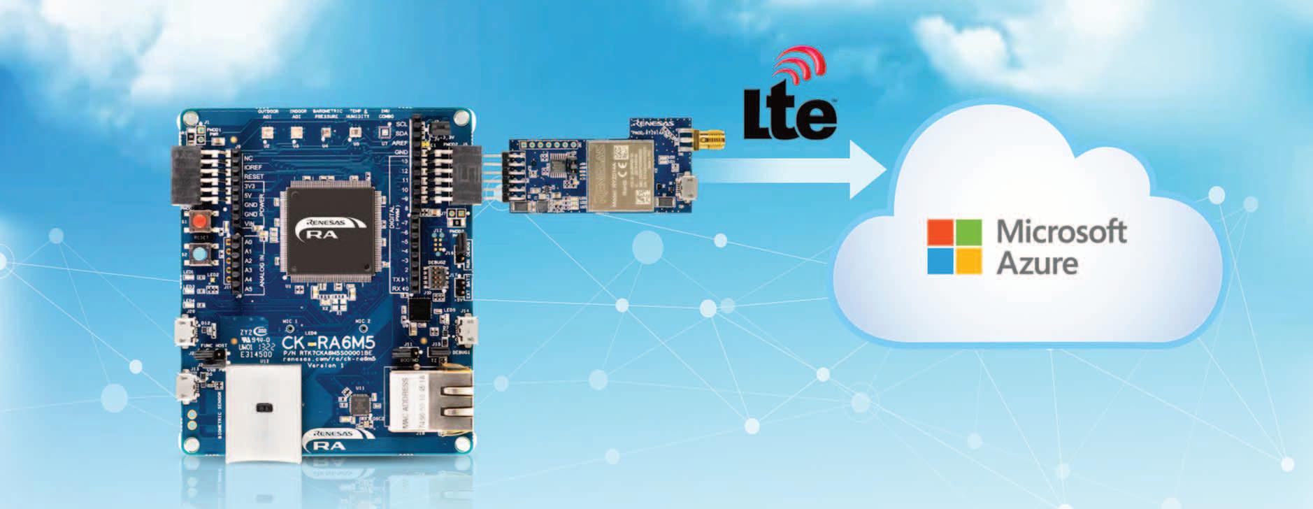
To ensure reliable functionality and interoperability, both CK-RA6M5 and CKRX65N kits have been certified by Microsoft Azure. This means that the devices are validated to connect with
Azure IoT Hub and can be securely provisioned through the Device Provisioning Service. Additionally, both devices are IoT Plug and Play-certified, enabling developers to integrate the devices into their solutions using pre-defined device models. This eliminates the need to manually configure hardware.
The Renesas Cloud Kits include a high-performance MCU, the RYZ014A Cat-M1 Pmod, six on-board sensors, and extensive peripherals, including a USB FS connector, USB-to-UART serial converter, two Pmod connectors, and a battery connector. For additional layers of security, Renesas collaborated with its partner, Crypto Quantique to implement a softwarebased IoT cryptography platform that securely connects IoT devices to serverhosted applications on-premises or in the cloud. Hardware-based security such as the Renesas Secure Crypto Engine 9 (SCE9) and Trusted Secure IP (TSIP) driver has been incorporated on the RA6M5 and RX65N MCUs respectively.
Renesas’ Cloud Kits make it easy to collect data from onboard sensors, upload them to the cloud for AI/Machine Learning processing and tools, and download the model back to the end point. Simplified development software is available out-ofthe-box, including Reality AI Tools and Edge Impulse Studio. Reality AI Tools provide a
true endpoint AI for a range of applications, including anomaly detection and voice recognition. The Edge Impulse Studio integrated cloud environment enables end-to-end AI/ML development using the kits’ accelerometer for asset and package tracking use cases.
Renesas MCU Leadership
Renesas is the industry’s #1 supplier of MCUs, shipping more than 3.5 billion units per year, with approximately 50% of shipments serving the automotive industry, and the remainder supporting industrial and Internet of Things applications as well as data center and communications infrastructure. Renesas has the broadest portfolio of 8-, 16- and 32-bit devices, delivering unmatched quality and efficiency with exceptional performance. As a trusted supplier, Renesas has decades of experience designing smart, secure MCUs, backed by a dual-source production model, the industry’s most advanced MCU process technology and a vast network of more than 200 ecosystem partners. For more information about Renesas MCUs, visit renesas.com/MCUs
For more information about Renesas cloud solutions, please visit: renesas.com/cloudsolutions
Renesas Electronics Corporation www.renesas.com

Mouser Electronics Inc., the New Product Introduction (NPI) leader empowering innovation, is pleased to sponsor the Connect for Good: Low Power Wireless Sustainability Challenge, presented by Nordic Semiconductor and Wevolver, going on now through 12 October. Entrants are encouraged to submit a project that utilises low-power wireless technology to solve various issues related to the United Nations Sustainable Development Goals, including clean energy and sustainable cities among others.
The first 100 entries will receive a free Nordic Semiconductor nRF9160 Development Kit for low power cellular loT. The grand prize winner will receive:
• Up to $20,000.
• One year subscription to nRF Cloud Services for up to 500 devices.
• Soracom connectivity for each device. Soracom is a global provider of smart IoT connectivity, offering a cloud-native wireless service designed specifically for the needs of connected devices.
• Support from Crowd Supply to get the winning design to market. Crowd Supply is a launchpad for open hardware, hackables and high-end goods that embrace the principles of open design.
"Mouser is excited to partner with Nordic on this initiative. Our company has a legacy of empowering innovation and creativity in engineers, makers and students," said Kevin Hess, Senior Vice President of Marketing at Mouser Electronics. "We support the entire product development process, through supplying individual components and kits, as well as providing design tools, services and resources.”
“The winning design will be an innovative product that is energy-efficient, helps fight climate change, protects ecosystems, or is beneficial to society,” said Geir Langeland, EVP Sales and Marketing at Nordic Semiconductor. “We are excited to have the support of Mouser which is committed to encouraging engineering innovation for the future.”
Each project should incorporate the Nordic Semiconductor nRF9160 DK low-power hardware platform as part of the design. The challenge is open to all engineers and students, ages 18 and up, with sufficient engineering capability to develop a working prototype. Entries will be judged based on the technical and commercial feasibility of the solution, the level of innovation shown and the potential impact on the selected UN Sustainable Development Goals (Goals 7, 11, 13 and 15).
Nordic Semiconductor is also offering technical support and education for entrants, including Nordic Developer Academy, an online learning platform, and one-on-one technical support through Nordic DevZone
For more information on how to enter, eligibility rules, judging criteria and other terms and conditions, please visit https://www.wevolver.com/article/connect-forgood-low-power-wireless-sustainability-challenge/.
■ Mouser Electronics | www.mouser.com
u-blox and Position Partners, an Australasian provider of intelligent positioning solutions, have announced the expanded coverage of the PointPerfect global navigation satellite system (GNSS) augmentation service to Victoria and New South Wales, including Melbourne and Sydney, as an initial step in rolling out the service to the Australian and New Zealand markets.
Access to industry-standard high accuracy positioning for fleet and Internet of Things applications
Available via Thingstream, u-blox’s enterprise-grade IoT service delivery platform, PointPerfect is the first PPP-RTK (Precise Point Positioning, Real-Time Kinematic) high-precision positioning solution commercialized in the region. PointPerfect adopts the global industry driven SPARTN messaging format that enables the highly efficient transfer of GNSS correction data.
The collaboration between Position Partners and u-blox will facilitate the rollout of accurate positioning for a diverse range of applications, from autonomous shuttles and public transport to service robots and other Internet of Things (IoT) uses.
At last year’s IGNSS Conference in Sydney, Position Partners presented the results of a case study in Melbourne, where PointPerfect was tested in an urban setting on e-scooter micro mobility devices.

■ u‑blox | www.u-blox.com/en
SEGGER’s embOS is a preemptive RTOS, designed to be the foundation for developing embedded applications. Now in its 4th decade of continuous use and enhancement, its reliability and performance underpin the firmware in every J-Link and JTrace. Visit here for information on testing embOS on the STM32C011-DK board
SEGGER’s Embedded Studio is the leading multi-platform IDE. Characterized by its flexibility of use, it includes all the tools and features a developer needs for professional embedded C and C++ programming & development. Under SEGGER’s Friendly License, Embedded Studio can be downloaded without registration and be used free of charge for educational and non-commercial purposes, as well as be evaluated on all platforms without code size, feature, or time limitations. An Embedded Studio CPU support package containing project templates and system files for the STMicroelectronics STM32C0 series is available.
The STM32C0 series is also supported by embOS-Ultra, SEGGER’s high-performance RTOS. embOS-Ultra uses Cycleresolution Timing for greater precision and time resolution than any other RTOS on the market. Switching to embOSUltra immediately enhances performance and saves power. It also gives the application the option to use both cycle-based and microsecond-based timing. API is compatible to traditional embOS, making migration easy with no application changes required and with traditional RTOS behavior maintained. embOS-Ultra simply provides Cycle-resolution Timing where new additional API calls are used. There is no need to choose between the traditional and the revolutionary. https://www.segger.com/evaluate-our-software/ https://www.segger.com/evaluate-our-software/st-microelectronics/st-stm32c011-dk/
■ SEGGER | www.segger.com
Navitas Semiconductor, the only pure-play, next-generation power semiconductor company, will introduce and display an expanded portfolio of leading-edge gallium nitride (GaN) and silicon carbide (SiC) power products at Europe’s prestigious PCIM 2023 conference. Featuring over 400 international technical papers, with a comprehensive technology and application-focused conference program, PCIM –which takes place in Nuremberg, Germany, from 9th to 11th May – is Europe’s leading event for professionals involved in the fields of “power, control and intelligent motion”.
Visitors to the Navitas exhibition booth (Hall 9, #525) will discover how GaN and SiC deliver the advanced performance, functionality, reliability and ease-of-use demanded by next-generation EV, solar, energy storage, home appliance and industrial drives. Highlights include GaNFast™ power ICs that integrate GaN power, sensing and control in a single device, and robust, high-voltage, high-efficiency GeneSiC™ SiC semiconductors optimized for reliable operation in harsh-environment, high-power designs.

“PCIM is a key event in the power-electronics calendar,” says, Alessandro Squeri, Navitas’ senior director for European sales “Continuing our ‘Electrify our World™’ mission, Navitas’ demonstrations, papers and panel discussions provide critical insight into how next-generation GaN and SiC deliver power-conversion and fast-charging solutions that could reduce global CO2 emissions by as much as six Gigatons per year by 2050.”
During this year’s conference Navitas will participate in the following sessions:
Tuesday 9th May
• “GaN Power ICs Drive Efficiency and Size Improvements in BLDC Motor Drive Applications.”, - 11:40am: GaN Devices Session, Brüssel 1, Alfred Hesener, Senior Director, Industrial Applications
• “GaN Power ICs Enable 300cc 700kHz 300W AC-DC Converter.”
- 11:40am: Power IC Session, München 2, Tom Ribarich, Senior Director Strategic Marketing
• “GaN-based High-Frequency, High-Power-Density, 2-in-1 Bi-directional OBCM Design for EV Applications.”
- Power Electronics for Electric Cars Poster Session, Foyer, NCC Mitte, Bin Li, Senior Applications Manager, for Minli Jia, Sr. Staff Applications Engineer
Wednesday 10th May
• “Wide Bandgap Design with GaN HEMT and Vertical GaN.” (panel)
- 1:05pm, Hall 7, #480, Stephen Oliver, VP Corporate
Marketing & Investor Relations
Thursday 11th May
• “Reliability and Quality Requirements for SiC and GaN Power Devices.” (panel)
- 12:10pm, Hall 7, #480, Stephen Oliver, VP Corporate
Marketing & Investor Relations
• “High-Frequency High-Efficiency LLC Module with Planar Matrix Transformer for CRPS Application Using GaN Power IC.”
- 2:20pm, DC-DC Converters Session, Brüssel 1, Bin Li, Senior Applications Manager
■ Navitas Semiconductor | www.navitassemi.com
Infineon Technologies and Hi-Lo Systems, a Taiwan based IC programming and testing company, announced their partnership in the area of Trusted Platform Module (TPM) security chips. Hi-Lo Systems has officially become an Associated Partner of Infineon in the Greater China market and will provide firmware update programming services for Infineon’s OPTIGA™ TPMs. This will help accelerate time-to-market for a wide range of device manufacturers.
Digitalization and the Internet of Things (IoT) have brought more intelligence and convenience to everyday life. At the same time, the information security requirements for devices have also increased. TPMs provide a secured platform for data and processes of embedded systems by creating and storing keys, and enabling the integrity of the device’s operating system and firmware. Infineon’s OPTIGA TPM series supports TCG TPM 1.2 and the latest 2.0 standards. It is the ideal choice for ICT, computer, server, and IoT security.
Device manufacturers very often need to decide how to cope with Operating System (OS) updates or the evolution of TPM versions. In order to make the best and most flexibly use of the chip inventories of different versions, device manufacturers may also need to perform firmware updates on the TPM. For them, performing firmware updates in their factories is an additional task that needs to be deployed. This is facilitated by the partnership between the two companies, in which Hi-Lo Systems provides industry-leading security programming technology to support the firmware updates for the full range of Infineon’s OPTIGA TPMs.
Hi-Lo Systems operates many locations around the world including more than 20 programming centers with secured programming zones that can help device manufacturers deploy TPM devices quickly and flexibly. This reduces the effort and cost of updating firmware, thereby accelerating the time-to-market and meeting the market’s demand for fast supply chains.
■ Infineon Technologies | www.infineon.com

Hi-Lo Systems supports Infineon’s OPTIGA™ TPM firmware programming to accelerate device manufacturers’ time-to-market
New from OMC, the pioneer in optoelectronics design & manufacture, Dual Status Profiled Backlights™ combine two colours of emitter in a single profiled backlight, enabling designers to use the single backlight source to indicate status very clearly, rather than a single colour backlight that is simply on or off. Dual Status Profiled Backlights provide a clean, bright and clear illumination for a display to ensure the machine-human interface is easy to understand. As robust components with an extended product life, Dual Status Profiled Backlights can be used in multiple applications and industries, including harsh environment applications such as the petrochemical industry (explosive gas detector systems, display systems for oil pipeline valves, gas and electricity metering) and in research, instrumentation and medical applications (life support system displays, imaging applications, measurement instrument displays).
Dual Status Profile Backlights bring benefits to industrial applications where colour backlights have not previously been a practical solution for displays, as they solve the additional cost and reliability issues around adding multiple LEDs to a backlight cost-effectively when custom dimensions are required. Dual Status Profiled Backlights are easy to drive, take up less space in a design and provide a cost-effective solution, even for small to medium volume requirements. The two colours indicate status very clearly and provide a way to attract attention even from an oblique angle. Temperature status is a common application, where the use of a red LED emitter alongside a green LED emitter, enables a fast “switch to red” warning.
Dual Status Profiled Backlights have individually addressable LED emitters, and available colours range through ultrabright blue, four greens, three yellows, orange, three reds and ultrabright white.
■ OMC | www.omc-uk.com
AMD-sponsored series continues the path for community members to learn, create and design with FPGA-based SoCs
element14, an Avnet Community, along with AMD recently launched Path to Programmable III; a free training program that includes an FPGA-based SoC development kit and a design/build phase where selected participants will have the opportunity to win up to $4000 in prizes.

Path III is the third session in the element14 Community’s structured FPGA-based system-on-chip (SoC) training. The first Path was held in 2018 and focused on programmable logic devices (PLDs) and featured the AVNET MiniZed development board, based on AMD’s Zynq-7000 SoC. Path II convened in 2019 and offered more advanced learning opportunities and featured the AVNET Ultra96-V2 development board, based on AMD’s Zynq UltraScale+ MPSoC.
Path III will double the fun by offering structured training on both the MiniZed and Ultra96-V2 boards. Each training track will be followed by a design/build phase. To spice up the competition, element14 Community is offering up to $4000 in prizes and four different design paths.
New Dual Status Profiled Backlights™ combine two colours in a single device for cost-effective, dual-colour status indication in displays
‘Path to Programmable III’
“The Path to Programmable series offers our members a unique opportunity for professional growth, and with programmable technology driving innovation in various industries, this training will equip participants with the knowledge and tools to advance their careers,” said Dianne Kibbey, Global Head of Community and Social Media for element14. “We are excited to see what our participants will create and look forward to the continued innovation that programmable technology will bring.”
After participants complete the training modules for the MiniZed and Ultra96-V2, they will design and build a project following one of four design paths:
• The Vision Path: Embedded/Machine Vision, Face Recognition, Accelerated AI Video, Image/Video Streaming
• The Core Technology Path: AI/Machine Learning, Connectivity, DSP, Ethernet

• The Market Path: Health, Home, Gaming, Industrial
• The Environmental Path: Dirt & Plants, Streets & Highways, Pets & Critters, Water & Oceans
Applications are now open through April 30. Participants will be announced on May 3. The training begins on May 12 followed by the design/build phase beginning on July 14. Winners will be announced in August 2023.
element14 Community will award the grand prize winner an MP720025 US Digital Oscilloscope and HP OMEN 17ck1020nr 17.3” Gaming Laptop of $1900 value. The runner-up will receive an MP720644 US CAL DU Oscilloscope of $1000 value. The third-place prize winner will receive a FLIR C3-X WIFI Thermal Imager of $600 value. The fourth-place prize winner will receive a FLUKE-175 ESFP Handheld Digital Multimeter of $400 value.
To learn more about Path to Programmable III, and to sign up to enter before April 30, please visit community.element14.com
■ element14 | www.element14.com

Mouser Electronics, Inc. announces a new eBook in collaboration with Apex Microtechnology, exploring the challenges and nuances involved in designing high reliability components. In An Engineer’s Guide to High Reliability Components, subject matter experts from Apex Microtechnology offer rich insights into the most difficult aspects of high reliability design. The eBook includes five detailed articles, covering topics including thermal management, hermetically sealed packaging, and silicon carbide.
New electronic devices are enabling significant performance improvements in industrial, medical, and aerospace applications. However, these critical industries require the highest levels of reliability; any technology failure could result in disastrous consequences. An Engineer’s Guide to High Reliability Components, the new eBook from Mouser and Apex Microtechnology, addresses the specific design challenges involved in analogue power electronics for high reliability devices. The eBook also includes product information for 10 relevant Apex Microtechnology solutions, connecting engineers with the specific components needed to improve the reliability of their device designs. The Power Operational (Linear) Amplifiers from Apex Microtechnology support applications that require high current and high voltage, with output currents ranging from 0.01 A to 100 A (peak) and slew rates of up to 3000V/μs. The power operational amplifiers are an ideal choice for precision power analogue applications including electrostatic/magnetic deflection and DC/servo motion control.
The new eBook from Apex Microtechnology and Mouser also features information on the SA310 Brushless DC Motor Driver. Leveraging silicon carbide MOSFET technology, the SA310 motor driver offers improved efficiency with 30 A continuous output per phase. The SA310 Brushless DC Motor Driver supports a range of applications including motor control, test equipment, power inverters, and variable frequency drives.
Apex Microtechnology’s range of products, available from Mouser, includes amplifiers, power modules, and evaluations kits.
■ Mouser Electronics | www.mouser.com
Energy harvesting PMIC from Nexperia enables environmentally friendly energy-autonomous low-power devices
Nexperia, the expert in essential semiconductors, announced an expansion to its range of Power ICs with Energy Harvesting solutions to simplify and enhance the performance of low-power internet of things (IoT) and other embedded applications. The NEH2000BY is a high-performance power management integrated circuit (PMIC) which recharges a battery or storage capacitor using energy harvested from ambient sources, such as light (which can be harvested using a photovoltaic cell). As a result, Nexperia’s NEH2000BY will enable the development of electronic devices that are self-powered, smaller, and environmentally friendly. Furthermore, this energy harvesting solution can help mitigate the environmental impact of the billions of batteries produced and discarded each year.

Nexperia’s NEH2000BY PMIC makes it much easier to design energy harvesting solutions which can be up to 20x smaller than other competing offerings and do not require manual optimization for individual applications. In addition, the PMIC was designed without inductors, simplifying PCB design, and significantly reducing overall BOM and board size, with a 12 mm² assembly area.
To achieve the highest conversion efficiency, energy harvesting solutions must be able to adapt as the ambient energy source fluctuates. The NEH2000BY performs Maximum Power Point Tracking (MPPT), an adaptive algorithm to optimize how it transfers harvested energy and to achieve optimum average conversion efficiency by up to 80%. This unique MPPT algorithm combines speed with accuracy, allowing the PMIC to adapt to environmental changes in less than a second. This is significantly faster than any other currently available solution and maximizes the amount of energy harvested over the course of a day, vastly expanding the number of application areas. Furthermore, due to its self-optimization functionality and ability to operate autonomously without the requirement for pre-programming, the NEH2000BY makes it easier for designers to power devices with ambient energy.
■ Nexperia | www.nexperia.com
Mouser Electronics, Inc., the New Product Introduction (NPI) leader™, equips engineers and agricultural professionals with an easy-to-navigate resource library focused on the latest advancements and technologies in the field of agriculture. From robotic solutions to embedded systems, Mouser’s comprehensive Smart Agriculture hub gives users access to a world of innovative products and solutions to further drive farming industries into the future. Mouser provides an expansive lineup of articles, blogs, products, eBooks and more, exploring topics such as vertical farming within smart cities, data fusion and building a smart greenhouse.
Mouser stocks the industry’s widest selection of semiconductors and electronic components, including the following solutions for smart agriculture applications:

• The IPW Series outdoor antennas by Linx Technologies provide a ground-plane independent, IP67-rated dipole antenna solution that mounts permanently to metallic and non-metallic surfaces. The Linx Technologies IPW Series outdoor antennas are available for cellular, Wi-Fi®, and LPWA / ISM frequencies and are ideal for remote sensor networks.
• The Eduponics mini kit from STEMinds is designed to demonstrate the integration of IoT and smart agriculture. The included board features onboard environmental sensors and supports the C programming language in the Arduino IDE environment and MicroPython in Thonny IDE.
• The T9501 from Amphenol Advanced Sensors is an IP67-rated humidity and temperature sensor that offers an advanced, cost-effective sensing solution for virtually any type of harsh-environment application. The T9501 sensor is based on a capacitive polymer sensor chip, and ASIC integrated into an easy-mount OEM package.
• The J Series 2835 Photophyll™ Select LEDs from Cree LED feature an advanced spectrum with blue and green output tuned for horticulture applications. The J Series 2835 Photophyll Select LEDs are designed to replace the white LEDs that are common in two-channel white + red horticulture luminaires. By maximizing green content and minimizing red content versus standard lighting LEDs, these devices enable significant enhancements to luminaire cost and performance.
To learn more about the latest solutions for smart agriculture, visit https://resources.mouser.com/agriculture/.

■ Mouser Electronics
www.mouser.com

IAR is announcing the launch of IAR Embedded Secure IP, enabling developers to add embedded security to their firmware applications even at a late stage of the product life cycle.
With IAR Embedded Secure IP, software managers, engineers, and project managers can rapidly upgrade their existing products with unique and flexible security at any point in the design, up to production and manufacturing. Customers can then choose from deploying the secured software themselves or initiate volume production with one of IAR´s approved partners, such as Hi-Lo Systems or EPS Global.
As security legislation and security requirements are becoming stricter, embedded developers need the flexibility to add security features to their product’s firmware application at any time of the product life cycle.
With IAR Embedded Secure IP, customers using MCU-centric systems do not have to revert their software development process. Still, they can easily integrate embedded security in their firmware applications, even at a late stage. The solution uses data obfuscation to protect sensitive data and program encryption from concealing the executable application. IAR Embedded Secure IP also implements the latest standards for operational data protection with digital signatures and device keys and allows for dynamic and customer-specific key creation, injection, and provisioning. Leveraging unique device identities or features provides cloning protection and safeguards the customer’s IP.
IAR Embedded Secure IP encrypts developers’ code and applications and transmits protected customer intellectual properties into the unique certificated device. IAR “Anticloning” generates unique identification for software applications and device hardware, which prevents counterfeits and over-production in manufacturing; “Active IP protection” ensures the security of customer intellectual properties such as applications, libraries, and other assets by providing encryption that guarantees safe device access.
For details on IAR Embedded Secure IP, please go to www.iar.com/eSecIP. More information about the IAR product portfolio for “Security Made Simple” is available at www.iar.com/security.
■ IAR Systems | www.iar.com
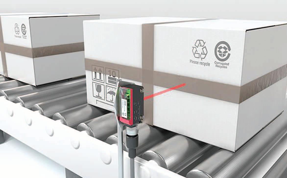
When carrying out presence control in automated intralogistics and packaging processes, the job of the sensor system is to safely detect the various objects. Handling of the sensor, including mounting, alignment and adjustment, must also be quick and simple, especially as a large number of sensors often need to be installed. This is why a) standardization and b) adaptation of the sensor to the individual needs of the customer are extremely important for the cost-effective commissioning of a system. We have developed an optimized sensor generation for precisely these requirements:
The new 5B series. Highly economical. Perfect handling.
Advantages for you
■ Housing: New, compact housing (dimensions W × H × L: 11 mm × 32.4 mm × 20 mm) – installation-compatible with previous series – ideal for tight installation spaces.
Certified with degree of protection IP 67 and ECOLAB
■ Attachment and mounting: Fast attachment and easy mounting thanks to metal inserts with M3 thread
■ Commissioning: All-around visible 360° indicator LEDs for easy installation and status display. Fast alignment thanks to homogeneous and easily visible light spot

■ Optimal configuration: Easy alignment and adjustment to the application thanks to a user-friendly potentiometer
■ Safe detection of depolarizing objects: Optimized performance for the detection of reflective, shrink-wrapped, and shiny objects
■ Electrical connection: Adaptation to individual customer requirements thanks to different connection options (e.g., cable, M8 connector, pigtail,...)
■ Switching frequency: Improved switching frequency for throughbeam photoelectric sensors with up to 900 Hz for high performance and function reserve


■ Tamper protection: Light/dark switching takes place in a tamperproof manner through polarity reversal of the (cable) wiring
Available operating principles
Retro-reflective photoelectric sensor
Throughbeam photoelectric sensor
Caracteristici
Cost effective mounting
Diffuse sensors

The larger the number of sensors to be mounted on a conveyor line is, the more important the cost effectiveness aspect becomes with respect to the time and cost of mounting and commissioning.
The intelligent and simple fastening concept with two convenient M3 metal threads facilitates fast mounting for the user.
The small and compact housing design also makes installation in small spaces easier.
Depending on your individual preference or local installation situation, various connection types are available, e.g., with M8 connector, cable, or pigtail connector.
Fast and simple commissioning and alignment
360° indicator LEDs ensure easy installation and a clearly discernible status display. Simple alignment of the sensor through the easily visible light spot results in an additional time saving and therefore in a reduction in costs for the user.
Presence control in intralogistics using retro-reflective photoelectric sensors
The new 5B series is also available as a model with potentiometer for better fine adjustment of the sensor. The sensor can thus be quickly and easily adapted to new application conditions. Moreover, the light/dark switching of the switching output can be performed in a tamperproof manner via the wiring.
In conveyor and storage systems, it is often the case that pallets, cardboard boxes and other containers are wrapped in film, which can be challenging for the sensor system. With the new 5B series, we offer optimized models especially for this area of application. These sensors guarantee safe switching even with shrink-wrapped or shiny objects.
Requirement: In a logistics center, various containers and cardboard boxes are to be transported on roller conveyors that are positioned closely to each another. In addition, some cardboard boxes are shrink-wrapped in film. All objects must be reliably detected. During commissioning, the sensor must be fast and simple to install, align, and adjust. The light spot must be easy to see.
Solution: With their compact, space-saving housing, the new 5B series sensors can be mounted directly on roller conveyors that are positioned closely to each other. The sensors are installed and securely mounted using convenient metal inserts with M3 thread. They are aligned quickly and easily using a homogeneous and clearly visible light spot as well as 360° indicator LEDs. Adjustment is user-friendly by means of a potentiometer. Performance optimized for the detection of shrink-wrapped and glossy objects ensures that they can be reliably detected.
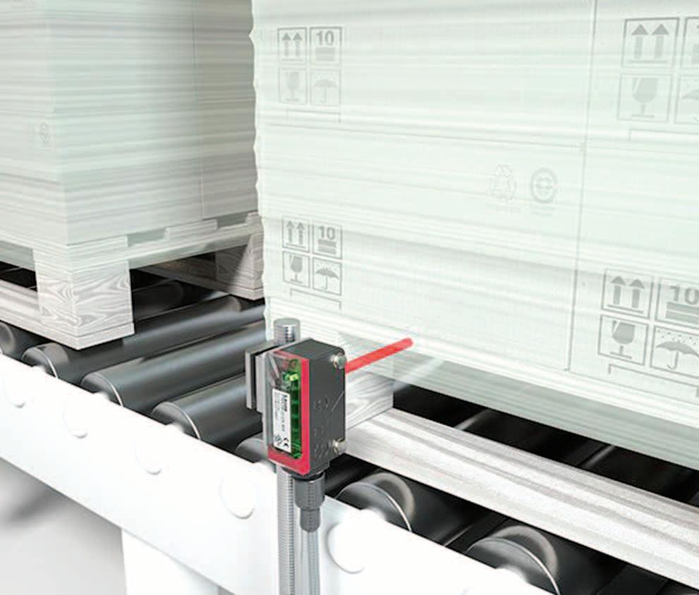

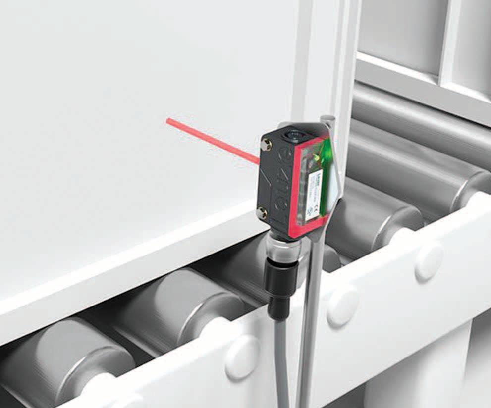
Presence control in packaging systems using throughbeam photoelectric sensors
Requirement: At a food manufacturer's plant, potato chips are packed in primary packaging. The packages are then transported further on a conveyor line where they are to be reliably detected. The light spot must be visible. The sensor state should also be visible from a distance of 2 m.
Solution: The new sensor of the 5B series can also be mounted horizontally on the conveyor line, and the light spot is easy to see. Thanks to the bright 360° indicator LEDs, the sensor state is visible at all times, even at some distance away from the conveyor line. The advantage of the throughbeam photoelectric sensor is the very high function reserve. This ensures reliable detection even in very demanding environmental conditions, and it reduces the risk of system downtimes. Furthermore, the new 5B series has an optimized switching frequency of 900 Hz.