


3/2022 A PAN EUROPEAN MAGAZINE https://international.electronica-azi.ro INTERNATIONAL

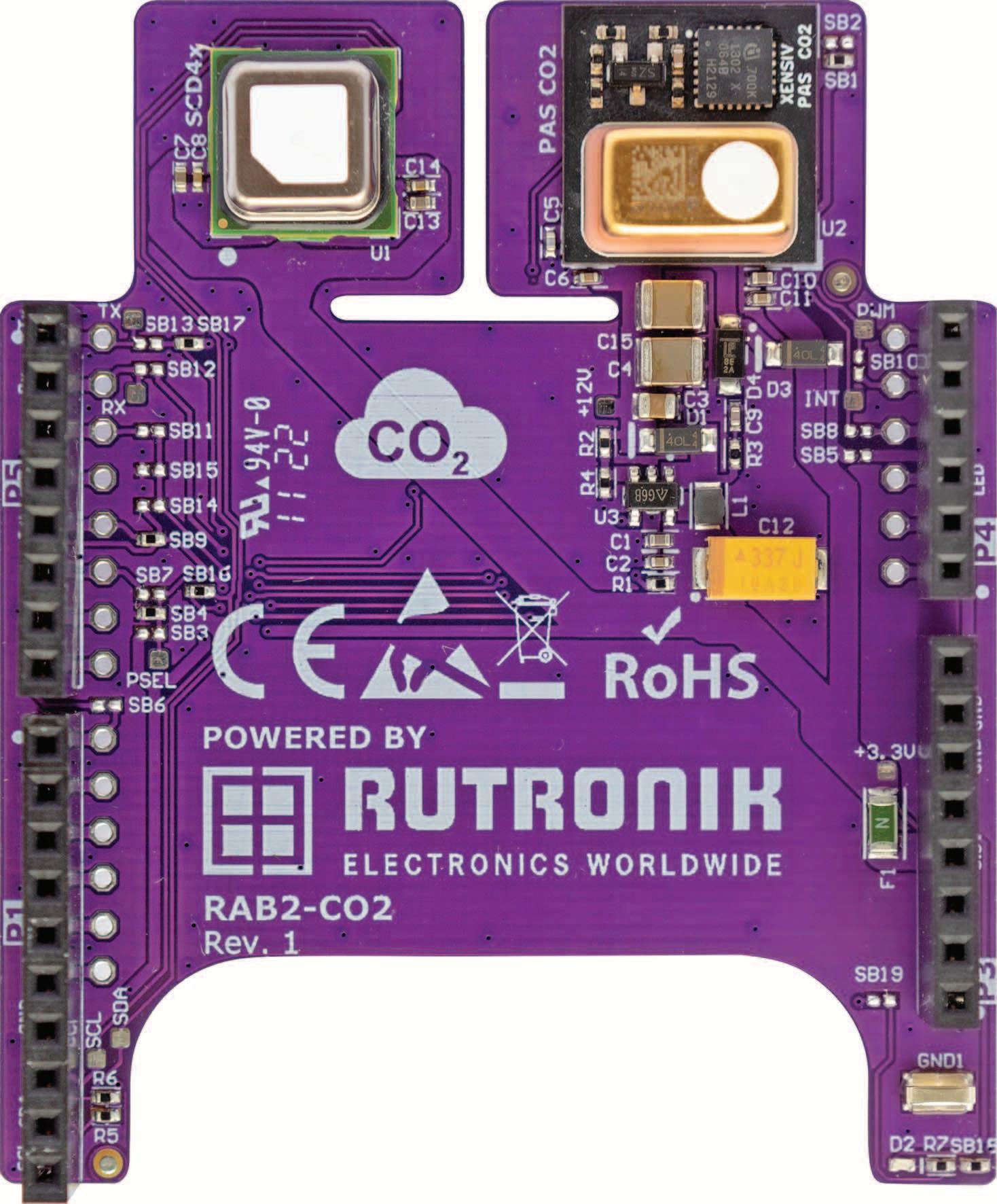
Reducing the pre-development phase with the Rutronik Adapter Board – RAB2 for CO2 Sensing from Rutronik System Solutions
Rutronik System Solutions expands the existing product portfolio with the new Adapter Board – RAB2 for CO2 Sensing. The board offers a unique approach using CO2 sensors, comparing two ultramodern sensors from Infineon and Sensirion. That provides the opportunity to use one board in the pre-development phase to evaluate which sensor suits a specific application most. As a result, the time-to-market for applications requiring CO2, relative humidity, and temperature measurement is significantly shortened.
CO2 measurements play an increasingly important role in the development of applications. For example, there is a growing demand for smart sensors to measure indoor air quality. They ensure real-time CO2 monitoring for ventilation systems, air purifiers, and thermostats and prevent, among other things, excessive CO2 concentration, which can harm health.
That is exactly where the new Rutronik Adapter Board – RAB2 for CO2 Sensing comes into play. Two state-of-the-art CO2 sensors, PASCO2V01 from Infineon and SCD41-D from Sensirion, are at the heart of the board. Both sensors operate on a photoacoustic measuring principle and impress with their compact design, among other things. Using the board, it is possible to test both sensors separately and compare them to each other in the pre-development phase. It enables developers to evaluate which sensor fits best for the respective application in the field of CO2, relative humidity, and temperature measurement and with which component the application development continues. Thanks to the combination of the components on only one board, a faster time to market is realizable.
Flexible combination and expandable thanks to the Arduino interface
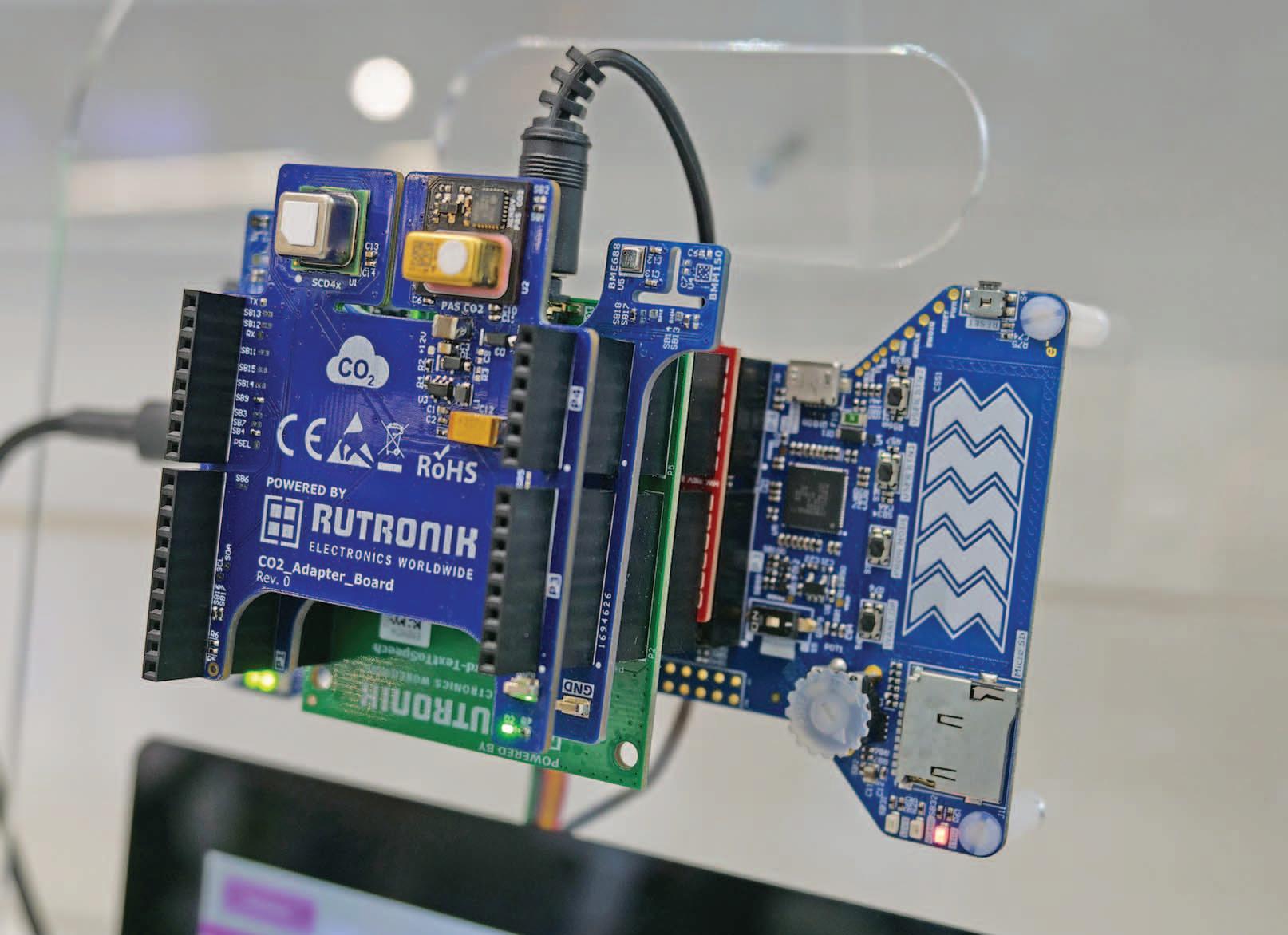
Like all other boards from Rutronik System Solutions, the Adapter Board – RAB2 for CO2 Sensing features an Arduino interface. That means that the board can easily combine with already developed boards such as the RDK2, Rutronik Adapter Board – Text To Speech, Rutronik Adapter Board – HMS Anybus, and the Rutronik Adapter Board – RAB1 Sensorfusion and embedded in a complex evaluation system.
The experts from Rutronik System Solutions also provide the corresponding software stacks. All components featured on the board are available in Rutronik’s product portfolio. That way, the distributor ensures that the components are currently and long-term available.
Further information about the Rutronik Adapter Board – RAB2 for CO2 Sensing and a direct contact option can be found at https://www.rutronik.com. An order option is also available on the e-commerce platform https://www.rutronik24.com.

Rutronik https://www.rutronik.com


https://international.electronica-azi.ro 3
PRODUCT NEWS
3 | Reducing the pre-development phase with the Rutronik Adapter Board – RAB2 for CO2 Sensing from Rutronik System Solutions
6 | Anritsu and CIG Jointly Demonstrating 800G Optical Transceiver PAM4 Test Solution at CIOE 2022
7 | New Industrial Gigabit Ethernet Transceivers Offer Precision Timing Protocol to Optimize Process Automation Functionality
8 | Healthcare and the cloud: secunet medical connect securely links medical devices and networks

Smart Building and Factory Automation

43 | Nexperia releases ultrafast 650 V Recovery Rectifiers for automotive and industrial applications
44 | The RDK2
9 | onsemi Silicon Carbide Technology Enables All-Electric VISION EQXX to Go Further on a Single Charge


10 | How to Leverage the Inverting Buck-Boost Topology in High Voltage Applications
46 | Encompassing Variety: Automation & Control at Digi-Key
49 | NXP Introduces High-Performance S32K39 Series MCUs for Modern Electrification Applications
50 | Get Smart about using Conductive Elastomers for Electrical Bonding in Mil -Aero Connectors
54 | Newest u-blox automotive multi-band GNSS module enables ADAS applications up to 105°C
14 | Cybersecurity threats on Endpoint AI systems

18 | How to Design a Modular Overlay Network for Industry 4.0 Data Processing Optimization in the IIoT
23 | Ready for take-off
28 | Maximizing Power Density With an innovative 5MHz LLC transformer driver
32 | Multiturn Position Sensor Provides TPO Capabilities (True Power-On) with Zero Power
36 | Power to Space Farming!
40 | Charging into the future
43 | Analog Devices Announces World’s First Long-Reach, Single-pair Power over Ethernet (SPoE) Solutions for
Management
Managing Director - I onela G anea
Editorial Director - Gabriel N eagu
Accounting - I oana P araschiv

Advertisement - Irina G anea
Web design - Eugen Vărzaru
Contributing editors

Cornel Pazara PhD. Paul S vasta PhD. N orocel C odreanu PhD. Marian Blejan PhD. B ogdan G rămescu
54 | Renesas Unveils First Family of Automotive Radar Transceivers with Industry’s Highest Accuracy and Lowest Power Consumption


55 | u-blox and GMV partner to develop market ready end-to-end safe positioning solutions for ADAS
56 | onsemi’s New Approach to Inductive Position Sensing Speeds Up Time-to-Market
56 | Renesas Lays Out Wi-Fi Roadmap Based on Technology from Celeno Acquisition
59 | Pre-assembled, tested, ready to connect
57 | Nexperia launches new hotswap Application Specific MOSFETs (ASFETs) with double the improvement in SOA
58 | 3.5” embedded board for IoT applications
58 | Fanless embedded PC for 10th generation Intel Core I processors
“Electronica Azi” is a registered trademark at OSIM - Romania, Registered position: 124259

ISSN: 1582-3490

Electronica Azi International | 3/2022 4
14 46 54 9 ®
Printed by Electronica Azi International is published 4 times per year in 2022 by Euro Standard Press 2000 s.r.l. It is a free to qualified electronics engineers and managers involved in engineering decisions. Copyright 2022 by Euro Standard Press 2000 s.r.l. All rights reserved. EURO STANDARD PRESS 2000 srl VAT: RO3998003 | Tel.: +40 (0) 31 8059955 | Tel.: +40 (0) 744 488818 office@electronica-azi.ro | https://international.electronica-azi.ro Electronica Azi International » TABLE OF CONTENTS

Anritsu and CIG Jointly Demonstrating 800G Optical Transceiver PAM4 Test
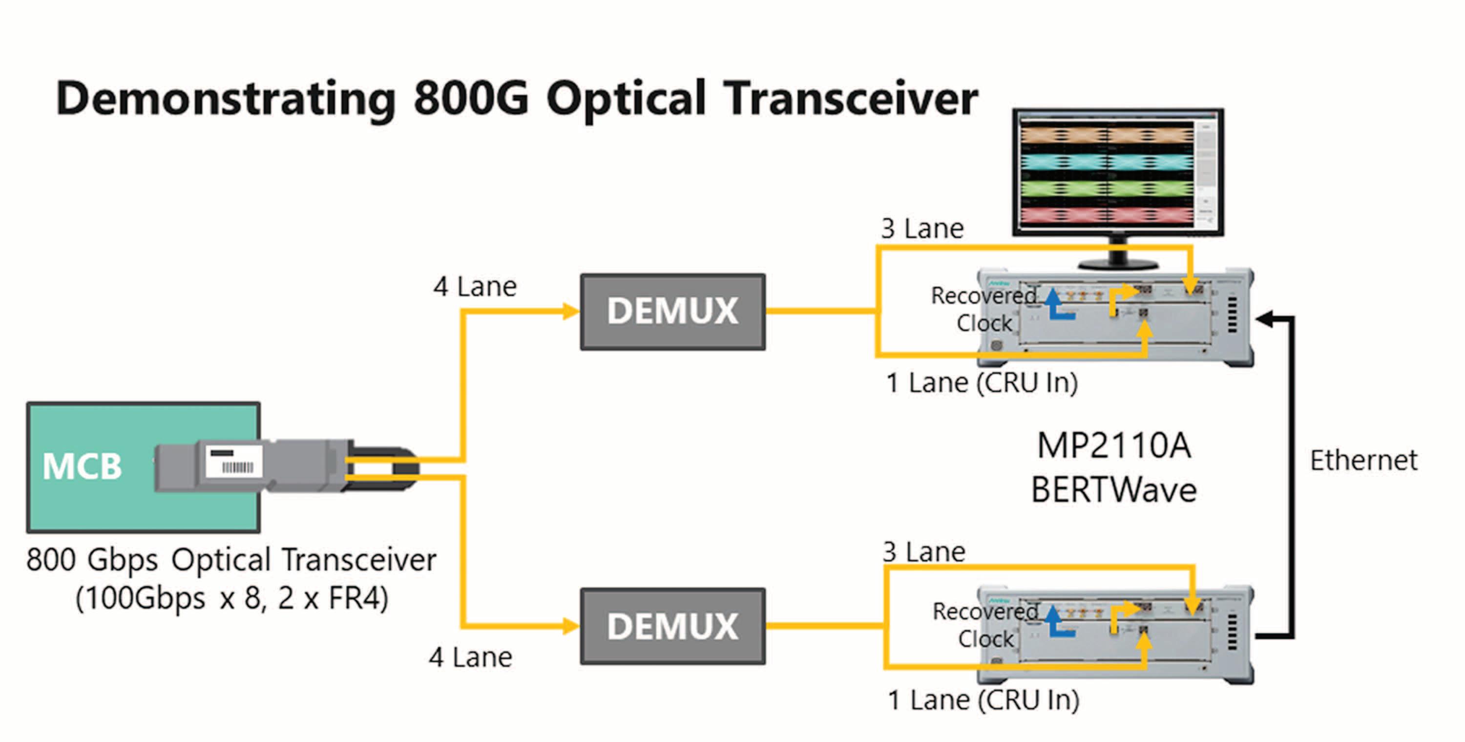
Solution at CIOE 2022
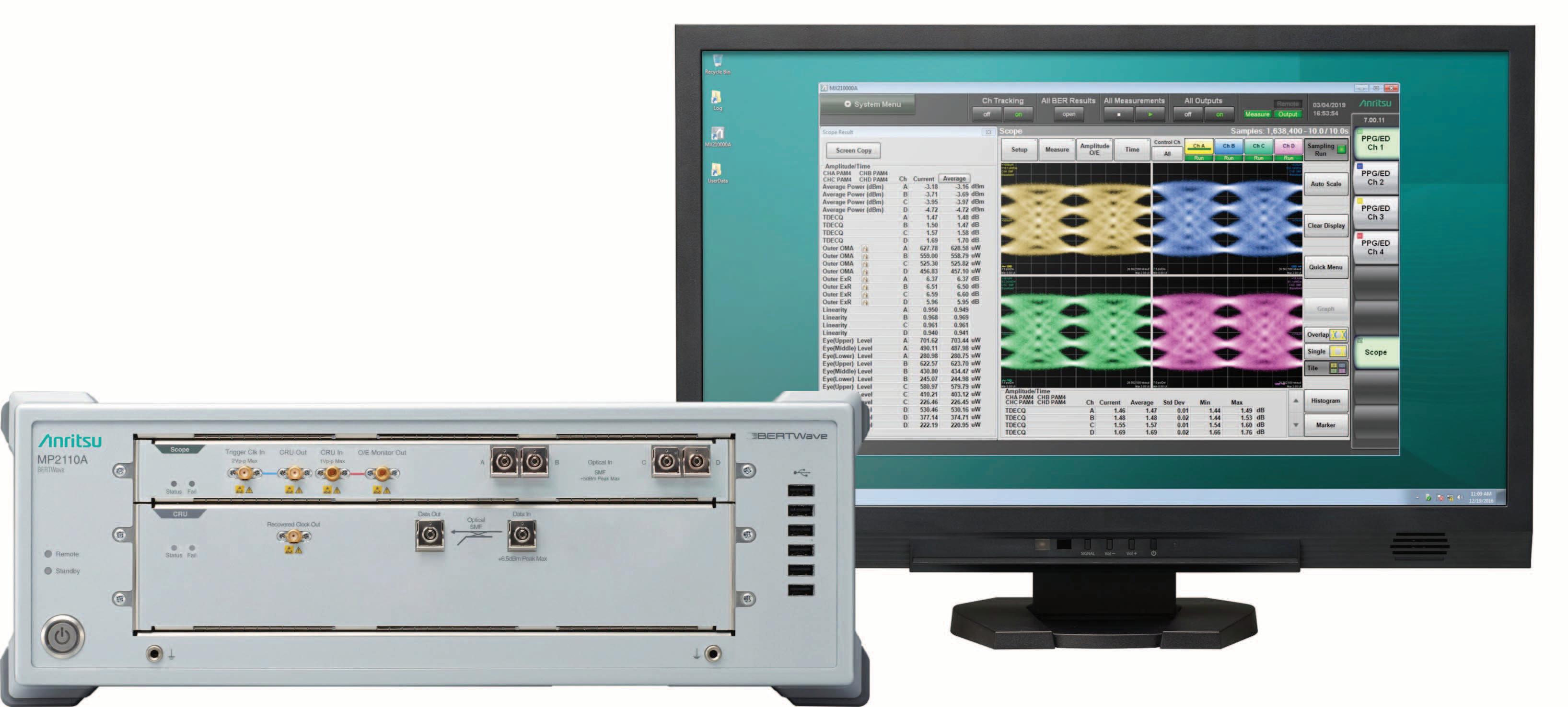
Anritsu Corporation (President Hirokazu Hamada) and CIG Photonics (CIG) are jointly demonstrating an 800G optical transceiver*1 PAM4 test solution in the Anritsu booth (#7B33) at CIOE 2022 to be held from December 7 to 9, 2022 in the World Exhibition and Convention Center, Shenzhen, China.
Additionally, to support expected rapid traffic increases caused by new future applications such as AI and machine learning, 800G optical transceivers are being developed, and first-generation 8lane 100 Gbps PAM4* 4 optical transceivers are now under test. With a built-in CRU*5, the MP2110A 4ch
The 800G transceiver under test is a CIG QSFP-DD800 2x400G-FR4 module. The optical interface conforms to 400GBASEFR4 interface using dual 53.125 Gbaud PAM4 CWDM.
The electrical interface conforms to 400GAUI-4 using 8-lane 53.125 Gbaud PAM4. The transmission distance is 2 km, and the max. power consumption is 16 W.
Technical Terms
*1 Optical Transceiver: Hot-pluggable device that E/O and O/E-converts electrical and optical signals for highspeed data transmission using electrical signals at device side and optical signals at optical-fiber side
*2 Lane: Number of optical-transceiver I/O channels.
*3 TDECQ: Abbreviation for Transmitter and Dispersion Eye Closure Quaternary; index for evaluating PAM4 optical signal quality.
*4 PAM4: Abbreviation for Pulse Amplitude Modulation; amplitude modulation technology for increasing transmission capacity. PAM4 transfers 2 bits of data as 4 levels in one time slot.
The test setup will input an 8-lane*2 optical signal from a CIG QSFP-DD800 2xFR4 800G optical transceiver to Anritsu’s MP2110A Sampling Oscilloscope to demonstrate measurement of key test parameters, including TDECQ*3. With the explosive increase in network traffic levels due to the spread of services such as 5G, IoT, etc., optical connections, including optical transceivers, within and between data centers (DCI) are being upgraded to 400GbE.
sampling oscilloscope is the ideal all-in-one solution for analyzing NRZ*6 and PAM4 Eye patterns of 10G-800G optical transceivers and devices. Combining a sampling oscilloscope and CRU in one tester facilitates easy and space-saving operation. This demonstration uses two MP2110A units to measure and analyze 800G optical transceiver 8lane optical signals in parallel and cuts evaluation times by 50%. Anritsu hopes this test solution will help revolutionize datacenter networks.
*5 CRU: Abbreviation for Clock Recovery Unit; function for generating trigger signal from input data signal. Although sampling oscilloscopes require a trigger signal synchronized to the data signal, a CRU permits observation of the waveform of transmission equipment without a trigger signal.
*6 NRZ: Abbreviation for Non-Return to Zero; one technology for transmitting digital data.
Electronica Azi International | 3/2022 6
Anritsu Corporation https://www.anritsu.com/en-gb
COMPANIES
New Industrial Gigabit Ethernet Transceivers Offer Precision Timing Protocol to Optimize Process Automation Functionality
Developers of industrial automation systems are looking to shift away from the reliance on proprietary solutions for process synchronization to standardbased solutions that offer broader compatibility and reduce design costs. To deliver critical process synchronization, Microchip Technology Inc. announces the LAN8840 and LAN8841 Gigabit Ethernet transceiver devices that meet IEEE® 1588v2 standards for Precision Timing Protocol. The LAN 8840/41 Ethernet devices are enabled with Linux® drivers and deliver flexible Ethernet speed options including 10BASE-T, 10BASE-Te, 100BASE-TX and 1000BASE-T. The LAN8840/41 devices can facilitate critical packet prioritization by providing high-speed time stamping that is then relayed between the various components to determine network latencies, accommodate for those latencies, and synchronize time amongst all connected devices. This functionality is key for process automation applications that require precise control production systems such as robotics, distributed sensors and cooling and mixing systems.
Designed with robust applications in mind, the LAN8840/41 devices can withstand extended industrial temperatures ranging from -40°C to +105°C.

“The new LAN8840/41 single-port transceivers round out our Time Sensitive Networking offering by providing the connectivity for end nodes in process automation applications,” said Charles Forni, vice president of the USB and networking business unit at Microchip. “These devices complement our existing Ethernet portfolio, providing our customers with an end-to-end network solution of components, development tools and support from Microchip.”
To help companies achieve sustainability goals by reducing a network’s power consumption, the LAN8840/41 offers features like Wake-on-LAN (WoL) and energydetect power-down mode. Additionally, Energy-Efficient Ethernet (EEE) delivers low-power idle and clock stoppage modes for optimal power performance.
Microchip is an established supplier of industrial-grade networking solutions, offering a broad portfolio of robust and
highly integrated products. The new LAN8840/41 devices are well suited for markets with applications requiring accurate and precise time stamping, such as gas and chemical processing, electrical distribution, and currency trade systems which must be proven to be in sync with the National Institute of Standards and Technology (NIST) for Universal Coordinated Time (UTC) within one millisecond or finer increments.
Development Tools
The LAN8841 Ethernet Development System (EDS) Daughter Card is designed to provide a modular addition to compatible Microchip host boards. This EDS Daughter Card, when paired with the PCIe® Networking Adapter, enables evaluation of the LAN8841 through any host supporting the PCIe interface. Linux drivers supporting Precision Timing Protocol (PTP4L) are available for the LAN8841 on Microchip’s GitHub repository.
Microchip Technology
https://www.microchip.com
https://international.electronica-azi.ro 7
PRODUCT NEWS
Healthcare and the cloud: secunet medical connect securely links medical devices and networks

congatec, S.I.E and secunet present edge gateway at MEDICA 2022
Data processing will shape day-to-day healthcare in the future. Providing a secure gateway for hardware, operating system and interface, secunet medical connect helps companies to implement digitalization for individual needs. With the “one box solution” developed by congatec, S.I.E and secunet, decentralized medical structures can be integrated quickly, agilely and securely.
Value-added alliance partners congatec, S.I.E and secunet attended MEDICA (Hall 3, Stand B50) to present their joint solution portfolio for securely connecting medical devices and networks with modern data-driven IT services and healthcare platforms. The edge gateway family secunet medical connect enables the use of secure and GDPR-compliant cloud applications.
Data room edge gateway
Hosting secure off-premise data rooms requires the integration of gateway platforms such as secunet medical connect into existing clinical networks. Solution providers can then implement their data-
driven services on these platforms. This starts with secure and legally compliant collection, processing and pseudonymization of machine and patient data that is then in a next step transferred to the cloud. Throughout this process, the medical networks must be protected at all times, and patient data must be processed securely and in accordance with all medical regulations, standards and norms. And not only within the applications, but also across the system and interfaces themselves. secunet medical connect offers comprehensive security, from the hardware to the secure execution environment.
A gateway platform for numerous digitization tasks
Providers of digitization solutions for the healthcare sector such as Honic (Health Data Technologies GmbH) rely on secunet medical connect. The company offers a GDPR-compliant medical health data platform that enables data-based research and development. Applications from Honic are used on the edge gateway.
Complete development package for solution providers
The value creation alliance gives companies in regulated industries such as healthcare the opportunity to react quickly and agilely to new requirements in product development and shortens development cycles from concept to initial minimum viable products (MVPs).
These can be tested with end users in real-life Proof of Concepts (PoCs) to realize rapid market maturity of user-centric solutions.
Numerous industry-specific regulations and certifications are supported, including MDR-certified medical computers and cybersecurity standards.
Further information on the trade fair showcase of the value-added alliance partners congatec, S.I.E and secunet can be found at: https://www.congatec.com/en/congatec/events/medica/ congatec https://www.congatec.com
Electronica Azi International | 3/2022 8
COMPANIES
onsemi Silicon Carbide Technology Enables All-Electric VISION EQXX to Go
Further on a Single Charge
As part of a strategic collaboration with Mercedes-Benz, onsemi provides the carmaker with high-efficiency silicon carbide (SiC) power modules that increase the range of its VISION EQXX
onsemi (Nasdaq: ON), a leader in intelligent power and sensing technologies, today announced that Mercedes-Benz adopted onsemi silicon carbide (SiC) technology for traction inverters as part of a strategic collaboration. onsemi’s VETrac SiC modules increase the efficiency and lowers the weight of the all-electric Mercedes-Benz VISION EQXX’s traction inverter, extending the electric vehicle’s (EV’s) range by up to 10%. The EV completed a 1,202 km (747 mile) trip from Stuttgart, Germany to Silverstone, England, holding the record for longest distance traveled on a single charge.
The VISION EQXX sets new standards for electric range and efficiency, while remaining sustainable and luxurious – and consuming less than 10 kWh of energy per 100 km (62 miles).

This was achieved by a benchmark drag coefficient of just 0.17, lightweight design, reduced rolling resistance and the use of a battery that stores 100 kWh in 50% less space (and with 30% less weight) than comparable batteries. Key to the unprecedented range is an electrical system that ensures that 95% of the energy stored in the traction battery reaches the wheels – a huge improvement over internal combustion engine (ICE) vehicles that are only able to achieve around 30%.
”In addition to its superior SiC technology delivering extended range, onsemi also provides assurance of supply for its SiC solutions, the necessary scale to support production and a broad portfolio of intelligent power and sensing solutions,” said Simon Keeton, executive vice president and general manager, Power Solutions
Group at onsemi. “The high efficiency of our SiC solutions allows customers to avoid trade-offs between the cost of the battery and the range of the vehicle.”
A core piece of differentiation is the expertise in packaging, which is critical for improving heat dissipation and increasing power output at a smaller footprint than the closest competitor, as well as reducing the weight and cost of a power module. onsemi is the only largescale supplier of SiC solutions with endto-end supply capability, which includes volume SiC boule growth, substrate, epitaxy, device fabrication, best-in-class integrated modules and discrete package solutions.
onsemi https://www.onsemi.com
https://international.electronica-azi.ro 9
PRODUCT NEWS
How to Leverage the Inverting Buck-Boost Topology in High Voltage Applications

Question
How can you easily select the right coil for high voltage inverting buck-boost topologies?

Answer
By using simplified duty cycle equations to plot the coil current ripple vs. the input voltage for the output voltage of our circuit, then validating the findings with LTspice®.
Introduction
A variety of topologies can be considered for applications that require the generation of a negative voltage rail, as illustrated in the article “The Art of Generating Negative Voltages.” 1 However, if the absolute voltage at the input and/or output can exceed 24V and the required output current can reach a few amperes, the charge pump and the negative LDO regulator are to be discarded due to their low current capability, whereas the size taken by their magnetic components causes the flyback and the Ćuk converter solutions to become quite cumbersome. As a result, under such conditions, the inverting buck-boost provides the best compromise between high efficiency and small form factor.
However, to reap these benefits, the operation of the inverting buck-boost topology under high voltage conditions must be fully understood. Before diving into such details, we will begin with a brief review of the inverting buck-boost topology. Then, we will compare the critical current paths of the inverting buckboost, buck, and boost topologies.
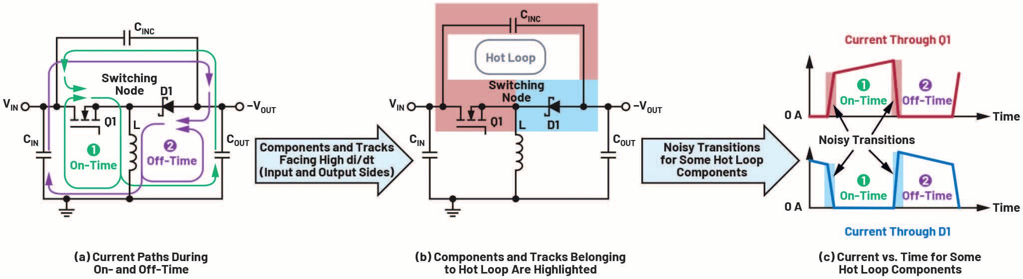
The three basic nonisolated topologies
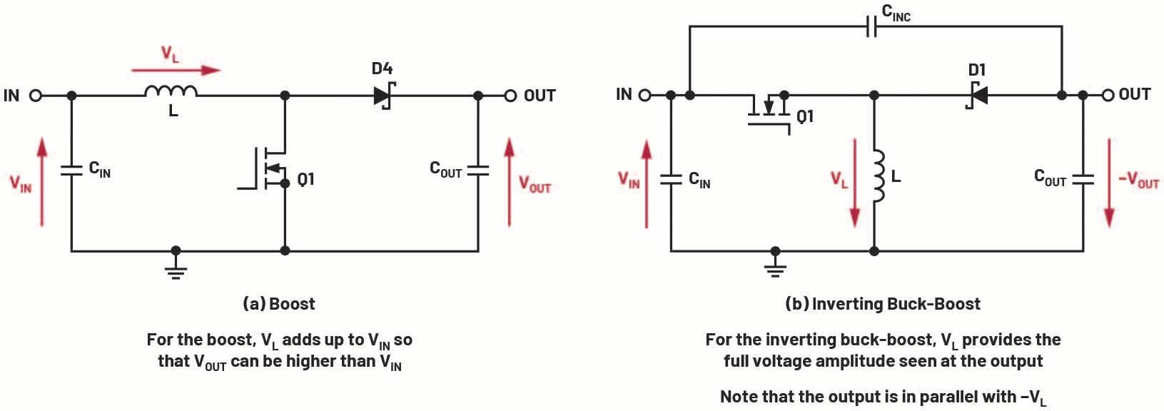
The inverting buck-boost belongs to the three basic nonisolated switching topologies. These topologies all consist of a
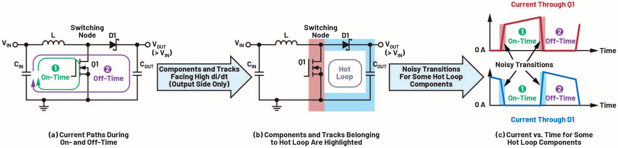
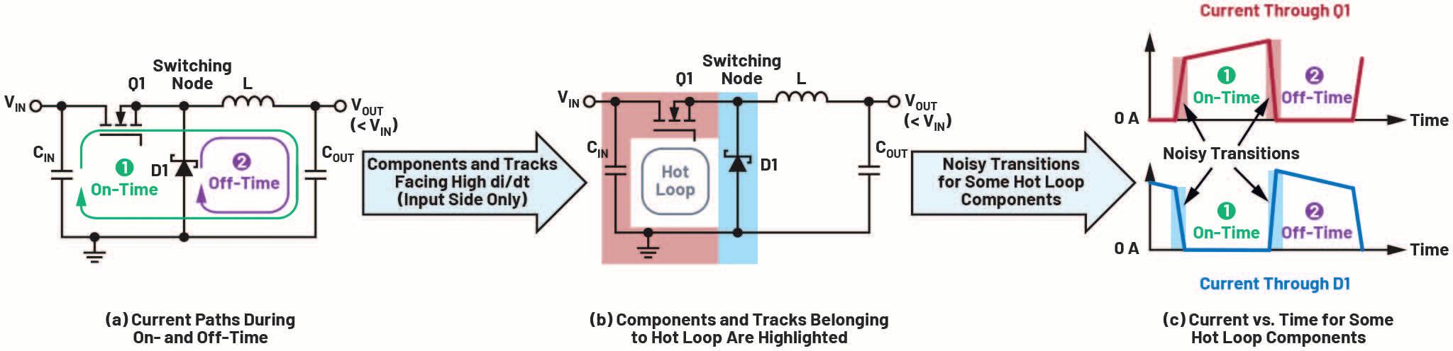
control transistor (usually a MOSFET), a diode (which can be a Schottky diode or an active diode – the synchronous MOSFET), and a power inductor as the energy storage element. The common connection between those three elements is referred to as the switching node. The positioning of the power inductor with regards to the switching node determines the topology. If the coil is located between the switching node and the output, we obtain the DC-toDC buck converter, which we simply call buck in the rest of this article. Alternatively, positioning the coil between the input and switching node creates the DC-to-DC boost converter, referred to as boost here.
Finally, the DC-to-DC inverting buck-boost consists of placing the coil between the switching node and ground (GND).
During each switching period and even in continuous conduction mode (CCM), all three topologies include components and PCB traces that are facing fast changes in current, leading to the noisy transitions highlighted in Figure 1c, Figure 2c, and Figure 3c. By keeping the hot loop small, the electromagnetic interference (EMI) radiated by the circuit can be reduced. At this stage, it is worth mentioning that the hot loop is not necessarily a physical loop through which the current circulates.
Electronica Azi International | 3/2022 10
© ADI
Components and tracks belonging to the hot loop – buck converter operating in CCM.
Figure 1
© ADI
Components and tracks belonging to the hot loop – boost converter operating in CCM.
Figure 2
© ADI
Components and tracks belonging to the hot loop – inverting buck-boost operating in CCM.
Figure 3
Author: Olivier Guillemant | Staff Central Applications Engineer Analog Devices
Indeed, for the respective loops highlighted in Figure 1, Figure 2, and Figure 3, the sharp current transitions do not occur in the same direction for the components and tracks highlighted in red and blue that form the hot loop.
For the inverting buck-boost operating in CCM represented in Figure 3, the hot loop consists of CINC, Q1, and D1. Compared with the hot loop of the buck and boost topologies, the hot loop of the inverting buck-boost contains components located both on the input and output sides. Among these components, the reverse recovery of the diode (or body diode if using a synchronous MOSFET) when the control MOSFET turns on generates the highest di/dt and EMI. Since a thorough layout concept is needed to contain the radiated EMI from these two sides, the last thing you want is to create additional radiated EMI through excessive coil current ripple by underestimating the required inductance of the inverting buck-boost under high input and/or output voltage conditions. This risk exists for engineers who rely on their familiarity with the boost topology to size the inductance of their inverting buck-boost circuit, as we now see by comparing both topologies.
Design considerations of inverting
Buck-Boost with high voltages
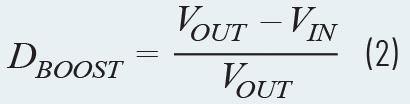
Both the boost and the inverting buckboost can generate an absolute output voltage whose amplitude is higher than the input voltage. There are, however, relevant differences between both topologies that can be highlighted with the help of their respective duty cycles in CCM, provided in Equation 1 and Equation 2. Please note that these are first-order approximations that do not consider effects such as the voltage drops through Schottky diodes and power MOSFETs.
We observe in Figure 4 that the duty cycle of an inverting buck-boost will exceed 50% from a much lower |VOUT| than the boost: 12V and 24V, respectively. It can be understood by referring to Figure 5.


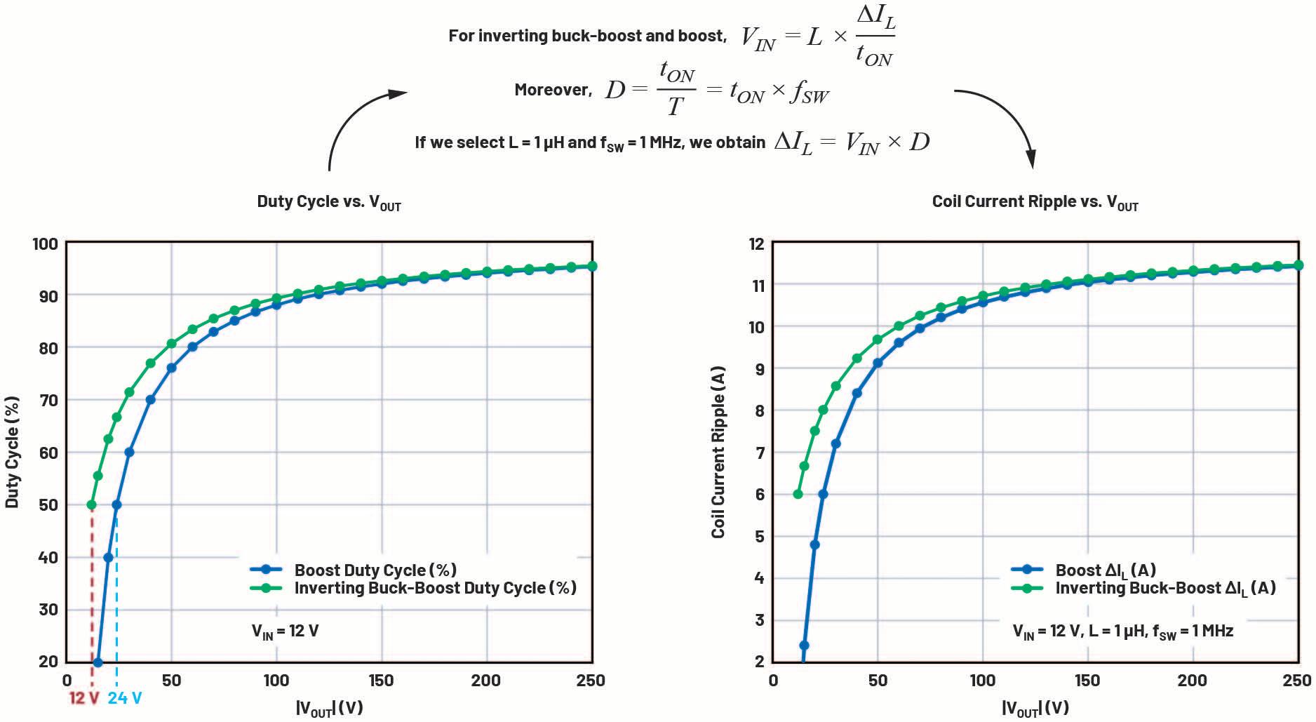
the achieved output voltage. On that occasion, the power inductor must provide much more energy to the output, which explains why the duty cycle already reaches 50% for a much lower |VOUT|.
The first-order approximation for the variation of these duty cycles vs. |VOUT| and with VIN = 12V is plotted on the left side of Figure 4. Moreover, assuming in both cases a switching frequency (fSW) of 1 MHz and an inductance of 1 μH for the power coil, the variation of the coil current ripple vs. VOUT was obtained on the right side of Figure 4.
In the case of the boost, the inductor is in the path between input and output. Therefore, the voltage through the power inductor (VL) adds up to VIN to provide the required VOUT. However, for the inverting buck-boost, VL is the sole contributor to
We can reformulate this observation by stating that, as the ratio |V OUT|/V IN decreases, the duty cycle drops much slower for the inverting buck-boost as for the boost.
https://international.electronica-azi.ro 11 DESIGN SOLUTIONS » High voltage inverting buck-boost topologies
© ADI
Duty cycle and coil current ripple vs. |VOUT| at VIN = 12V for inverting buck-boost and boost.
Figure 4
© ADI
Duty cycle and coil current ripple vs. VIN at |VOUT| = 48V for inverting buck-boost and boost.
Figure 6
© ADI
Impact of the coil positioning on the obtained output voltage
Figure 5
BUCK–BOOST CONVERTERS
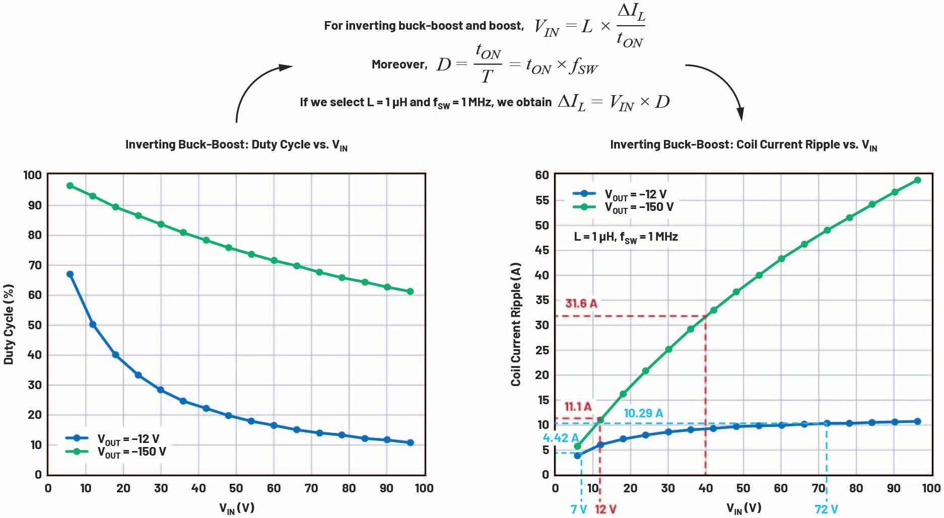
This is an important fact to consider during design, and its impact can be better understood by referring to Figure 6, where the first-order approximation of the duty cycle and coil current ripple are redrawn, but this time vs. VIN.
VIN increases by 62.5% from 48V to 78V. Since the decrease in D does not compensate for the increase in VIN, the coil current ripple increases significantly with VIN, as illustrated by the green curve on the right graph of Figure 6.
Selecting the inductance
When operating the LTC3896 in CCM, it is recommended to keep ΔIL between 30% and 70% of IOUT,MAX, which is 5A for our example. Consequently, we want to design for ΔIL between 1.5A and 3.5A over our whole input voltage range. Moreover, staying within this recommended range between 30% and 70% of IOUT,MAX means that we can only afford a ratio of up to 2.33 – that is, 70% divided by 30% – between the highest and lowest current ripple over our input voltage range. This is not a trivial task for a topology such as the inverting buck-boost where ΔIL varies significantly with VIN, as previously observed.
As demonstrated in Figure 6, the coil current ripple (ΔIL) is proportional to VIN and D. In the case of the boost, as VIN becomes higher than half of VOUT, the duty cycle decreases faster than VIN increases, going from 50% at VIN = 24V to a quarter of this value at VIN = 42V for the blue curve on the left graph of Figure 6. Consequently, ΔIL decreases quickly for VIN above 24V for the boost on the right graph of Figure 6. However, for the inverting buck-boost, we previously saw in Figure 4 that D decreases very slowly when |VOUT|/VIN decreases or, said differently, when VIN increases for a fixed |VOUT|. This can be seen for the green curve on the left graph of Figure 6, where the duty cycle loses only 25% when
Overall, the higher coil current ripple potentially faced under high voltage conditions by the inverting buck-boost compared with the boost explains why the former topology requires higher coil values if operating at the same fSW. Let’s use this knowledge in a concrete case with the help of Figure 7, which is, as well, based on first-order approximations.
Application with wide input voltage range and high output current
Let’s consider an application with VIN = 7V to 72V and VOUT = –12V at 5A. Given the high output current, we opt for a synchronous controller (LTC3896) to achieve high efficiency.
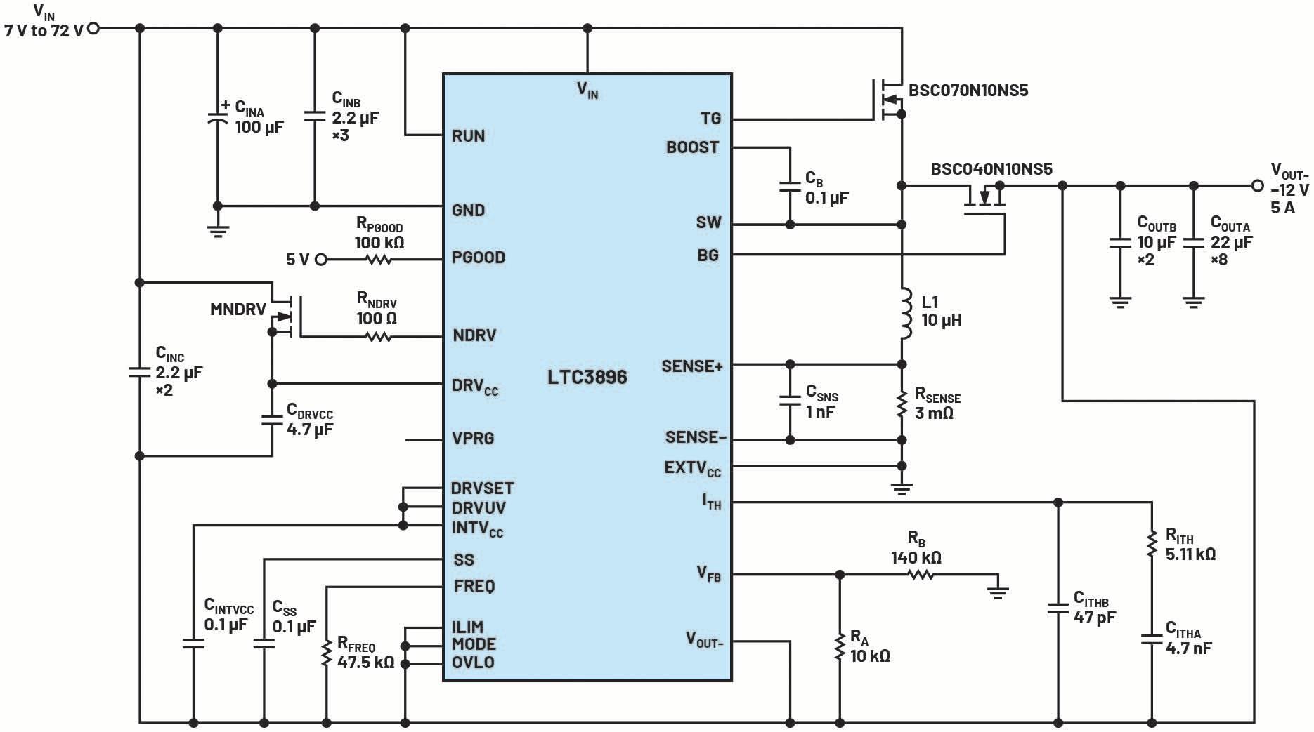
Referring to Figure 7, when using fSW = 1 MHz and L = 1 μH, the coil current ripple would vary between 4.42A and 10.29A, which is far too much. In order to position the lowest Δ IL to our recommended lower limit of 1.5A or 30% of IOUT,MAX, we need to reduce the existing value of 4.42A by a factor of three. This can be achieved by setting fSW to 300 kHz with a 47.5 kΩ resistor at the FREQ pin and selecting a 10 μH inductance. Indeed, this scales down ΔIL by (1 μH × 1 MHz)/(300 kHz × 10 μH) = 1/3.
Thanks to this scaling, the coil current ripple (ΔIL) should now vary between about 1.5A and 3.4A (between 30% and 68% of IOUT,MAX) over the whole input voltage range, which is just within the recommended range. We obtain the circuit provided on the last page of the LTC3896 data sheet, which is reproduced in Figure 8.
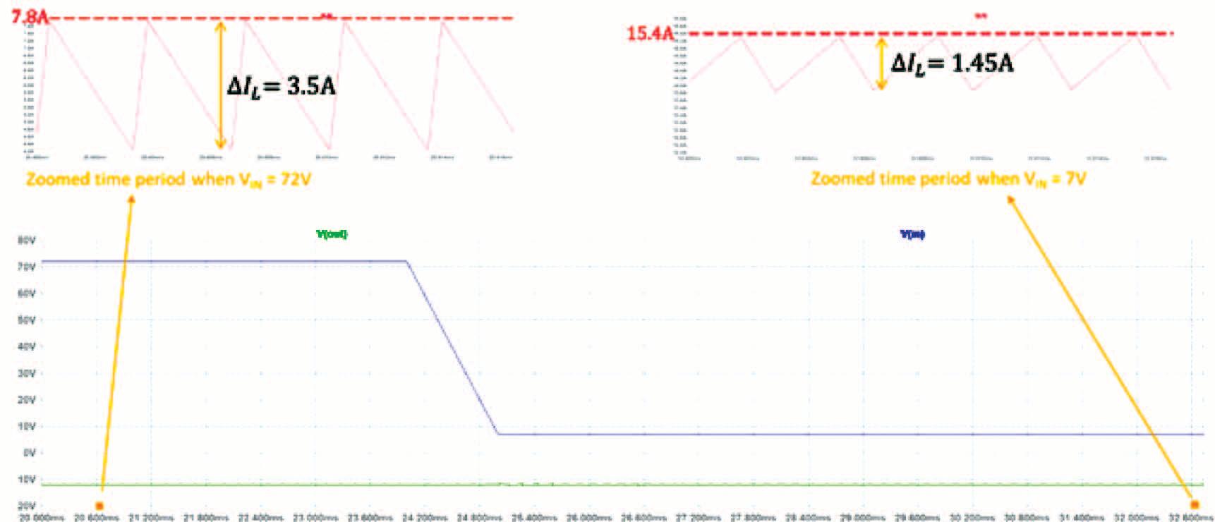
Validating our inductance selection with LTspice
Regarding the coil current ripple, more accurate values can be obtained by simulating the same LTC3896 circuit with LTspice, as demonstrated in Figure 9. In Figure 10, ΔIL equals about 1.45A and 3.5A, respectively, at VIN = 7V and 72V, which is consistent with the first-order approximation values previously extracted with the help of Figure 7 and the scaling of the fSW and L. Please note that the coil current probed in Figure 10 is considered positive when flowing towards RSENSE
An additional benefit of the LTspice simulation is to determine the peak coil current faced during operation, which is obtained at the lowest input voltage of 7V. As seen in Figure 10, our application will face a peak coil current close to 15.4A. By knowing this value, a power inductor with a high enough current rating can be selected.
Electronica Azi International | 3/2022 12
Duty cycle and coil current ripple vs. VIN at VOUT = –12V and –150V for inverting buck-boost. © ADI
Figure 7
LTC3896 circuit with VIN = 7V to 72V, VOUT- = –12V and fSW = 300 kHz.
© ADI
Figure 8
Designing with even higher output voltages
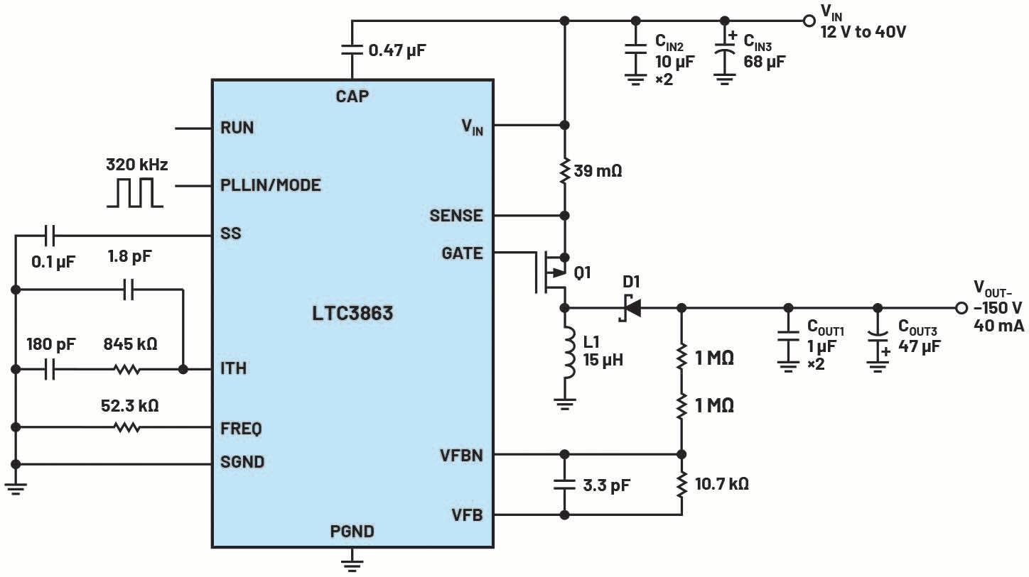

If we return to Figure 7, the current ripple values were also provided for a hypothetical case with a VIN range from 12V to 40V and a VOUT equal to –150V.
The first remark is that the current ripple is getting significantly higher for higher VOUT when keeping the same fSW and L. Such high ΔIL are often unacceptable, therefore, we would have to apply a higher scaling down factor compared with the previous example, which means a higher inductance for the same fSW. The second remark refers to the variation of ΔIL over the whole input voltage range. For the previous example with VOUT = –12V, ΔIL was only increasing by about 2.33 from lowest to highest ripple with the input voltage increasing more than tenfold. For the present case with VOUT = –150V, ΔIL already increases by 2.85 from lowest to highest current ripple, and this despite the input voltage only increasing by a factor 3.33 from 12V to 40V. Luckily, such challenges only exist in CCM. When in discontinuous conduction mode (DCM), limitations such as 30% to 70% of IOUT(MAX) no longer apply. It would anyway be too strenuous to convert VIN = 12V to VOUT = –150V at IOUT(MAX) = 5A in a single step. In any case, when such voltage conversions are required, the output current requirement is generally low, meaning that we operate in DCM. This is, for example, the case for the circuit on the last page of the LTC3863 data sheet, reproduced in Figure 11. Due to the low DC currents, using a nonsynchronous controller such as the LTC3863 was good enough to provide an acceptable efficiency under these conditions. In the case of this LTC3863 design in DCM, the LTC3863 circuit provided with LTspice is a nice tool to optimize the coil selection.
Conclusion
The hot loop of the inverting buck-boost topology includes components located both on the input and output sides, making its layout more difficult to implement than the buck and the boost topology. Although there are some analogies to the
About the author
boost, the inverting buck-boost faces much more current ripple under similar application conditions because its coil constitutes the only source of energy to the output (if we ignore the output capacitance).
For inverting buck-boost applications with
Olivier Guillemant is a central applications engineer at Analog Devices in Munich, Germany. He provides design support for the Power by Linear™ portfolio for European broad market customers. He has held various power application positions since 2000 and joined ADI in 2021.

He received his M.Sc. in electronics and telecommunications from University of Lille, France. He can be reached at olivier.guillemant@analog.com
high input and/or output voltages, the coil current ripple is potentially even higher. To contain it, higher inductance values are used compared with the boost topology.
A practical example was used to demonstrate how to quickly scale the inductance based on the application conditions.
■ Analog Devices www.analog.com

https://international.electronica-azi.ro 13
An LTC3863 circuit with VIN = 12V to 40V, VOUT- = –150V and fSW = 320 kHz. © ADI
Figure 11
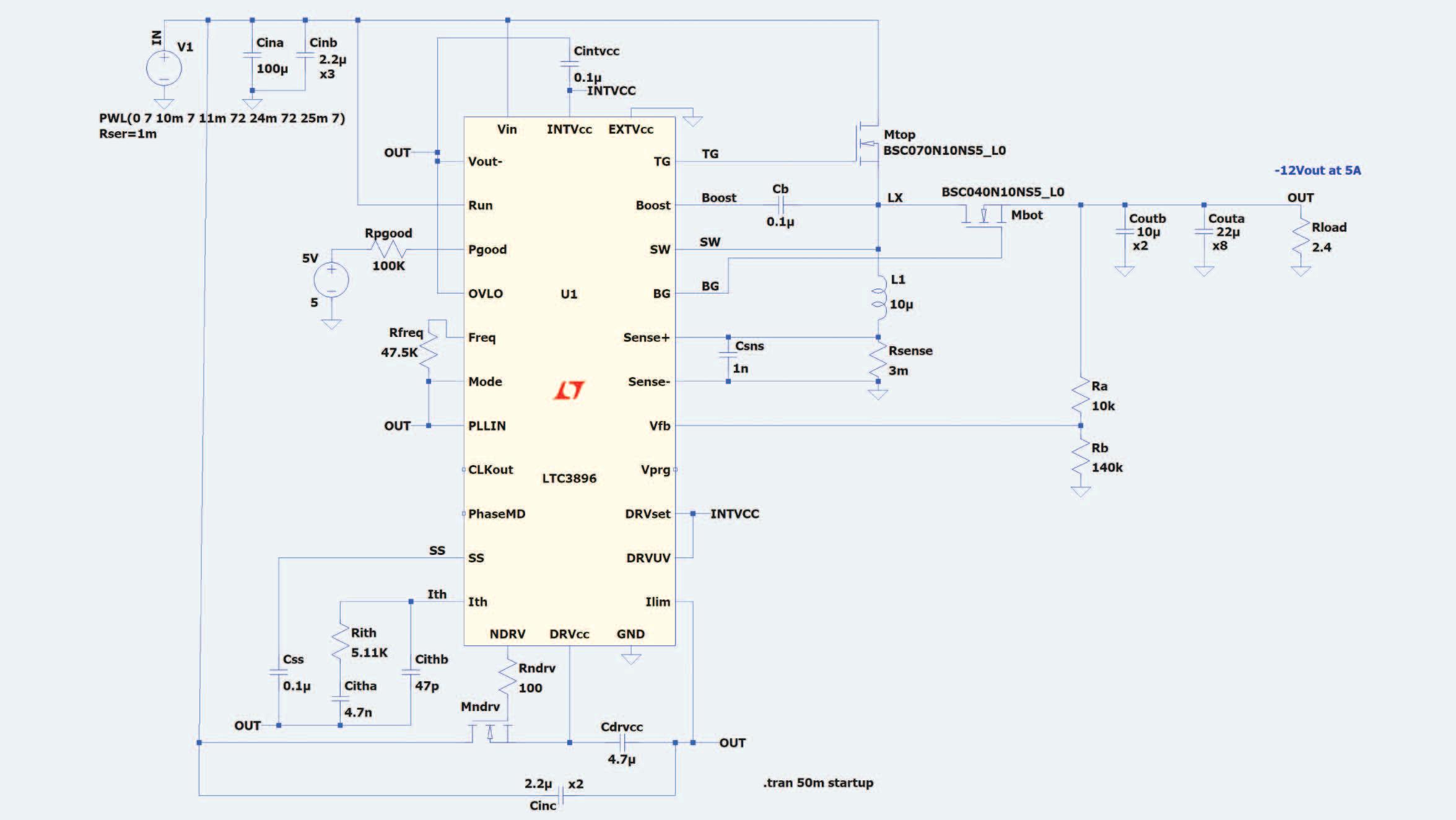
Figure 9 LTC3896 circuit simulated with LTspice © ADI
Measuring ΔIL at VIN = 7V and 72V and extracting the peak coil current with the previous LTspice circuit.
© ADI
1)Dostal,
DESIGN SOLUTIONS » High voltage inverting buck-boost topologies https://ez.analog.com
Figure 10
Frederik. “The Art of Generating Negative Voltages.” Power Systems Design, January 2016.
Cybersecurity threats
On Endpoint AI systems
With endpoint AI (or TinyML) being in the infancy stages and
slowly getting adopted by the industry, more companies are incorporating AI into their systems, such as for predictive maintenance in factories or keyword spotting in consumer electronics. But with the addition of an AI component into your IoT system, new security measures must be considered.
 Author: Eldar Sido Product Marketing Specialist, IoT and Infrastructure Business Unit Renesas Electronics

IoT has matured to an extent where you can reliably release products into the field with peace of mind, with certifications such as PSA Certified™ that provide assurance that your IP can be secured through a variety of techniques such as isolated security engines, secure cryptographic key storage, and Arm® TrustZone® usage. Such assurances can be found on microcontrollers (MCUs) designed with security in mind with scalable hardware-based security features such as Renesas’s RA family. However, the addition of AI leads to the introduction of new threats that infest themselves into secure areas namely in the form of adversarial attacks

Adversarial attacks target the complexity of deep learning models and the underlying statistical mathematics to create weaknesses and exploit them in the field, leading to parts of the model, training data being leaked, or outputting unexpected results. This is due to the black-box nature
of deep neural networks (DNN), where the decision-making in DNNs is not transparent i.e., “hidden layers” and customers are unwilling to risk their systems by the addition of an AI feature, slowing AI proliferation to the endpoint. Adversarial attacks are different than conventional cyberattacks as in traditional cyber security threats, security analysts can patch the bug in source code and document it extensively. Since in DNNs there is no specific line of codes you can address, it becomes understandably difficult.
Adversarial attacks in pop culture can be seen in Star Wars. During the clone wars, Order 66 can be viewed as an adversarial attack where the clones behaved as expected throughout the war but once they were given the order, they turned, leading to a tide in the war.
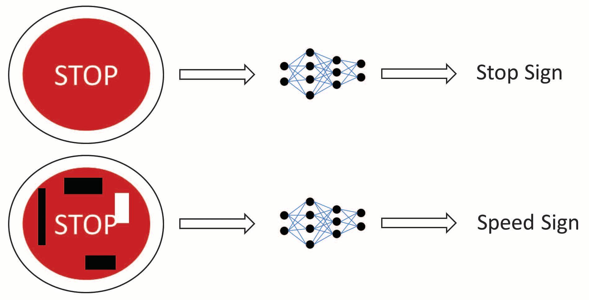
Notable examples can be found throughout many applications, such as a team of researchers taping stickers onto stop signs causing the AI to predict it as a speed sign[1]
Such misclassification can lead to traffic accidents and more public distrust in using AI in systems. The researchers managed to get 100% misclassification in a lab setting and 84.8% in field tests, proving that the stickers were quite effective.
The algorithms fooled were based on convolution neural networks (CNN), so it can be extended to other use cases using CNN as a base such as object detection and keyword spotting.
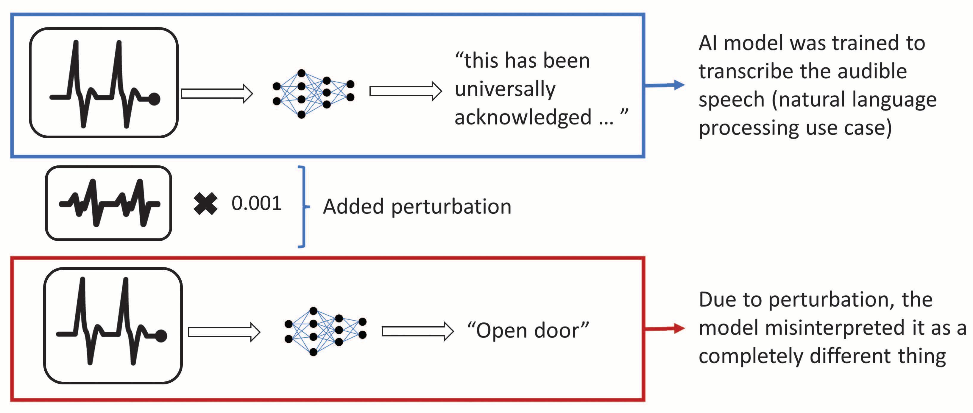
Another example by researchers from the University of California, Berkley showed that by adding noise or perturbation into any music or speech, it would be misinterpreted by the AI model to mean something other than the played music or transcribe something completely different, yet that perturbation is inaudible to the human ear[2].
This can be maliciously used in smart assistants or AI transcription services.
Electronica Azi International | 3/2022 14
The researchers have reproduced the audio waveform that is over 99.9% similar to the original audio file but can transcribe any audio file of their choosing at a 100% success rate on Mozilla’s DeepSpeech algorithm.
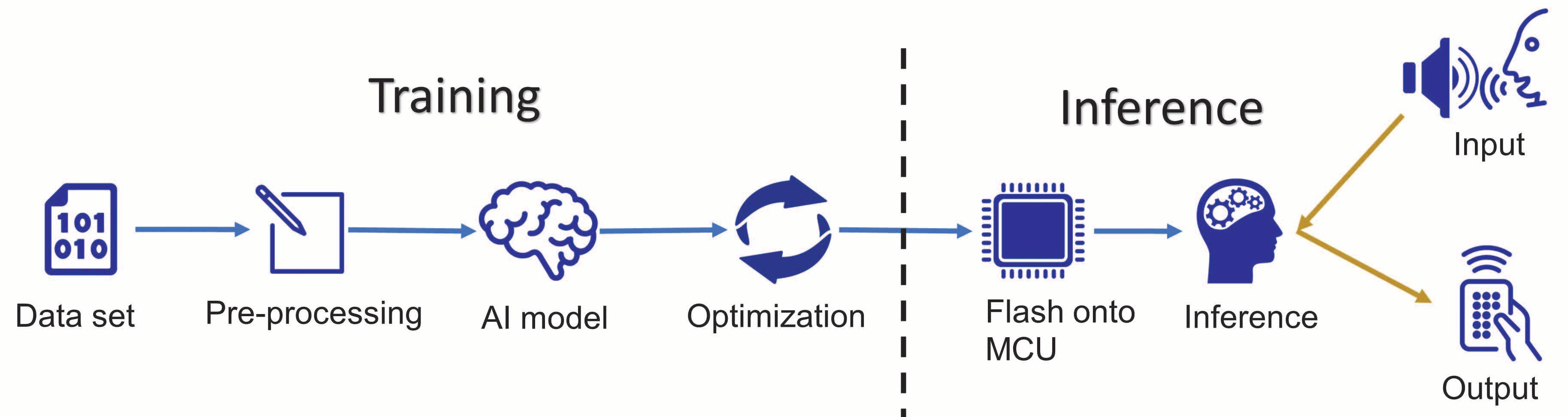
Where initially, the training is done offline, usually in the cloud, followed by the final polished binary executable flashed onto the MCU and used via API calls. The workflow requires a machine learning engineer and an embedded engineer.
Adversarial attacks can occur in either training or inference phases. During training, a malicious attacker could attempt “model poisoning” which can be of targeted or untargeted types. In targeted model poisoning, an attacker would contaminate the training data set/AI base model resulting in a “backdoor” that can be activated by an arbitrary input to gain a particular output yet works properly with expected inputs. The contamination could be a small perturbation that does not affect the expected operation (such as model accuracy, inference speeds, etc.) of the model and would give the impression that there are no issues.
This also does not require the attacker to grab and deploy a clone of the training system to verify the operation as the system itself was contaminated and would ubiquitously affect any system using the poisoned model/ data set. This was the attack used on the clones in Star Wars.
Untargeted model poisoning or Byzantine attacks is when the attacker intends to reduce the performance (accuracy) of the model and stagnates the training. This would require returning to a point before the model/data set has been compromised (potentially from start).
Types of Adversarial attacks
To understand the many types of adversarial attacks, one must look at the conventional TinyML development pipeline as shown in figure 3.
Since those engineers tend to work in separate teams, the new security landscape can lead to confusion on responsibility division between the various stakeholders.
Other than offline training, federated learning, a technique where data collected from the endpoints is used to retrain/improve the cloud model is intrinsically vulnerable due to its decentralized nature of processing, allowing attackers to partake with compromised endpoint devices leading to the cloud model becoming compromised.
This could have large implications as that same cloud model could be used throughout millions of devices.
https://international.electronica-azi.ro 15
Stickers taped on to STOP sign to fool the AI into believing it is a speed sign, the stickers (perturbations) are used to mimic graffiti to hide in plain sight.
Figure 1
© Renesas
By adding a small perturbation, the model can be tricked to transcribe any desired phrase.
Figure 2
© Renesas
End-to-end TinyML workflow. Figure 3
© Renesas
DESIGN SOLUTIONS » Renesas’s RA family
During the inference phase, a hacker can opt for the “model evasion” technique where they iteratively query the model (e.g., an image) and add some noise to the input to understand how the model behaves. In such a manner, the hacker could potentially gain a specific/required output i.e., a logical decision after tuning their input enough times without using the expected input. Such querying could also be used for “model inversion”, where the information about the model or the training data is extracted similarly.
Risk analysis during your AI TinyML development
For the inference phase, adversarial attacks on AI models is an active field of research, where academia and industry have aligned to work on those issues and developed
“ATLAS - Adversarial Threat Landscape for Artificial-Intelligence Systems!”, which is a matrix that would allow cybersecurity analysts to assess the risk to their models. It also consists of use cases throughout the industry including edge AI. Learning from the provided case studies will provide product developers/owners an understanding on how it would affect their use case, asses the risks, and take extra precautionary security steps to alleviate customer worries. AI models should be viewed as prone to such attacks and careful risk assessment needs to be conducted by various stakeholders.
For the training phase, ensuring that datasets and models come from trusted sources would mitigate the risk of data/model poisoning. Such models/data should usually be provided by reliable software vendors. An ML model can be also trained with security in mind, making the model more robust such as a brute force approach of adversarial training where the model is trained on many adversarial examples and learns to defend against them.
Cleverhans an open-source training library is used to construct such examples to attack, defend and benchmark a model for adversarial attacks, has been developed and used in academia. Defense distillation is another method where a model is trained from a larger model to output probabilities of different classes rather than hard decisions making it more difficult for adversary to exploit the model. However, both of those methods can be broken down with enough computational power.
Keep your AI IP safe
At times, companies would worry about malicious intent from competitors to steal the model IP/feature that is stored on a device on which the company has expended R&D budget on. Once the model is trained and polished, it becomes a binary executable stored on the MCU and can be protected by the conventional IoT security measures, such as protection of physical interfaces to the chip, encryption of software, and using TrustZone. However, an important thing to note, even if the binary executable would be stolen, it is only the final polished model that is designed for a specific use case that can be easily identified as a copyright violation, and reverse engineering would require more effort than starting with a base model from scratch.
Furthermore, in TinyML development, the AI models tend to be well-known and open-sourced such as MobileNet, which can then be optimized through a variety of hyperparameters. The datasets, on the other hand, are kept safe, as they are valuable treasures that companies spend resources to acquire and are specific for a given use case. Such as, adding bounding boxes to regions of interest in images. Generalized datasets are also available as open source such as CIFAR, ImageNet, etc.
They are good to benchmark different models on, but tailored data sets should be used for specific use case development. For instance, for visual wake word in an office environment, a dataset secluded to an office environment would give the optimum result.
Sum Up
As TinyML is still growing, it is good to be aware of various attacks that can occur on AI models, how they could affect your TinyML development, and specific use cases. ML models have now been attaining high accuracies but for deployment, it is important to ensure your models are robust as well. During development, both parties (ML engineers and embedded engineers) share responsibility for cybersecurity matters, including AI. Where ML engineers would concentrate on attacks during training and embedded engineers would ensure protection from inference attacks.
For model IP, a crucial element is to ensure that training datasets are kept secured to avoid competitors’ ability to develop similar models for similar use cases. As for the executable binary i.e., model IP on the device, it can be secured using best-in-class IoT security measures that Renesas’s RA family is renowned for, making it very difficult to access secure information maliciously.

References
[1] Eykholt, Kevin, et al. “Robust physical-world attacks on deep learning visual classification” Proceedings of the IEEE conference on computer vision and pattern recognition. 2018.
[2] Carlini, Nicholas, and David Wagner. “Audio adversarial examples: Targeted attacks on speech-to-text”. 2018 IEEE Security and Privacy Workshops (SPW). IEEE, 2018.
■ Renesas www.renesas.com

Electronica Azi International | 3/2022 16
CYBERSECURITY THREATS

How to Design a Modular Overlay Network for Industry 4.0 Data Processing Optimization in the IIoT
This article briefly discusses the problems of connecting legacy equipment to the IIoT. It then introduces the architecture of the Snap Signal family of hardware and software tools from Banner Engineering and how it addresses those challenges. It presents examples of Snap Signal devices including the DXMR90 controller, associated converters, adapters and filters, as well as application considerations when implementing wired and wireless edge computing or cloud connectivity.
Author: Rolf Horn | Applications Engineer Digi-Key Electronics

Data processing optimization in Industry 4.0 and the Industrial Internet of Things (IIoT) systems to support lean manufacturing can be accomplished through condition monitoring, predictive maintenance, overall equipment effectiveness (OEE) analysis and tracking, diagnostics, and troubleshooting. The problem in many instances is that legacy equipment was either not designed to be connected or may use any of a number of a variety of communications protocols, making it expensive to replace them all. To ensure maximum effectiveness and obtain actionable machine data, it’s simpler and more cost-effective in many instances to implement an overlay network that can connect existing automation islands and legacy equipment.
Designing such an overlay network is a challenging undertaking. It requires a controller that can receive signals from sensors and other devices that use a variety of communications protocols, combine
those signals into a unified stream of useable data, and export that data to edge computing resources or the cloud. The system needs adapters that can connect directly to sensors, indicators, and other devices. Converters are needed to connect previously incompatible device types, including legacy equipment.
In addition, to ensure reliable operation, filters are required to protect data communications from electrical noise and transients. All of these components should meet IP65, IP67, and IP68 environmental standards for operation in industrial settings, and the solution needs to be easy and cost-effective to implement.
Connecting legacy equipment to the IIoT
Many factories predate the appearance of the IIoT and Industry 4.0, and it’s often not possible to interconnect all of the equipment and machines into a single network, resulting in islands of automation. Even if not isolated on an ‘island,’
legacy equipment can be difficult to interconnect as a result of inflexibility arising from the use of proprietary communication protocols, non-standard connectors and cabling, and other factors.
A Snap Signal IIoT overlay network can provide a quick, flexible, and cost-effective way to connect legacy equipment and islands of automation by capturing and converting various non-compatible data communications protocols into an easy to distribute standard, able to be delivered to edge or cloud compute resources for analysis and action (Figure 1).

There are several key components needed to deploy flexible and reliable IIoT overlay networks:
• Adapters to reroute wiring and link various equipment wiring schemes from sensors, indicators and other devices to a standard format used in the overlay network.
• Data converters to translate incompatible formats such as discrete, analog, and various digital formats found on legacy equipment or automation islands into standard protocols such as IO-Link or Modbus to enable centralized performance monitoring.
Electronica Azi International | 3/2022 18
Industry 4.0
• Filters to protect the data from corruption in electrically noisy industrial environments, improving signal integrity and reliability and reducing troubleshooting requirements.
• A programmable controller to consolidate data from multiple sources and
provide local data processing, as well as connectivity enabling legacy equipment and islands of automation to be integrated into the IIoT.
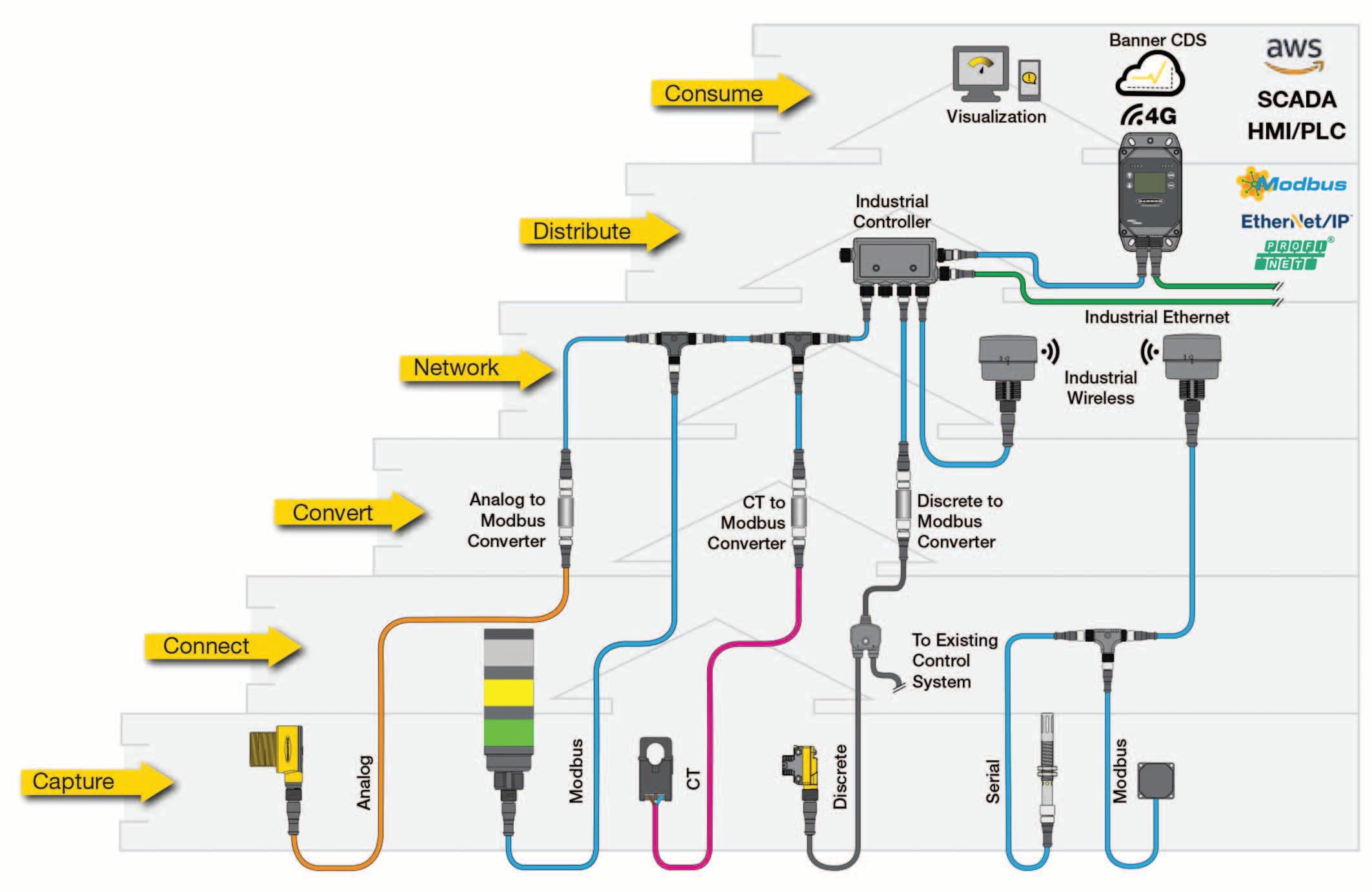
• A wired or wireless connection to distribute the collected data to edge computing resources and/or the cloud
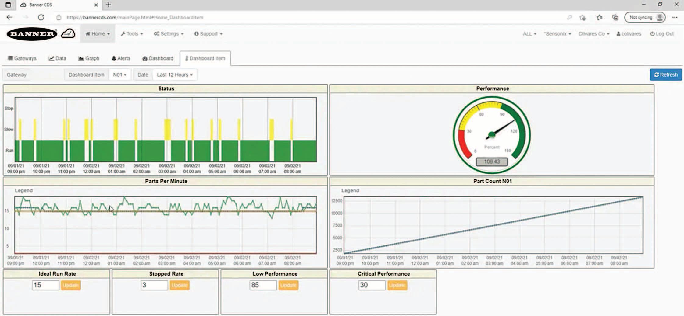
such as Banner’s Cloud Data Service (CDS), which provides data visualization and insights into machine performance and to send email or text alerts to support machine operation, maintenance, and repairs in real-time (Figure 2).
https://international.electronica-azi.ro 19 DESIGN SOLUTIONS » Modular Overlay Network
A Snap Signal overlay network provides a modular architecture to connect legacy equipment and islands of automation with edge or cloud computing resources.
Figure 1
© Banner Engineering
Consolidated data can be transmitted with a wired or wireless connection to edge computing resources or to the cloud such as Banner’s CDS (screenshot above).
Figure 2
© Banner Engineering
Controller for consolidating multiple data streams
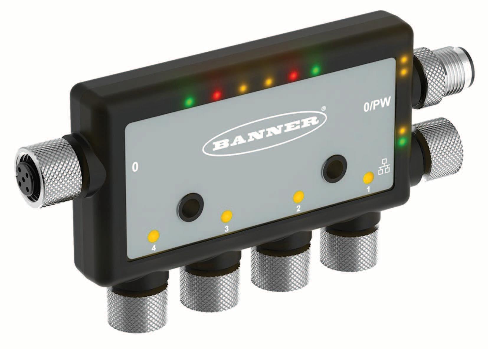
The programmable controller and data converters are key elements in designing an overlay network. The DXMR90 industrial controller from Banner serves as the central communications hub that combines signals from multiple Modbus ports into a unified data stream that is forwarded using industrial Ethernet protocols. For example, the model DXMR90-X1 includes four Modbus masters and supports concurrent communication with up to four serial networks (Figure 3).
Converters connect devices in IIoT networks
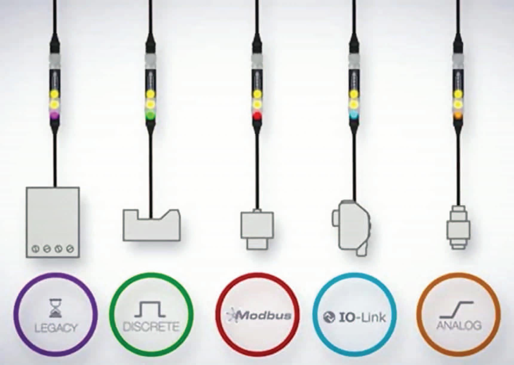
Efficient data conversion is needed to blend legacy equipment and islands of automation into an overlay network. For this function, designers can use Banner’s small plug-on S15C series in-line converters to convert condition monitoring and process-sensor data from a variety of formats into digital IO-Link data (Figure 4).
For example, the S15C-MGN-KQ is a Modbus master to IO-Link device converter that is user-configurable to read
they use the same power supply as the connected device. Use of S15C converters eliminates the 20-meter (m) IO-Link communication limitation since they can be installed at the end of a Modbus link, near the IO-Link master.
The S15C line of converters includes eight models:
• Six Modbus to IO-Link converters for use with Banner’s line of Modbus sensors, including ultrasonic, measuring light curtain, temperature/humidity, vibration/ temperature, and GPS. Plus, there is a generic converter that can be configured to enable most Modbus devices to be deployed as IO-Link devices.
Ports on the DXMR90 include a configurable Modbus port 0 (on the left side), Modbus master ports (1 to 4 on the bottom), configurable Modbus port 0/PW for RS-485 and incoming power (top right), and a D-coded Ethernet port (bottom right).
The DXMR90 is a highly integrated communications controller that features:
• The ability to work with a range of Modbus devices, converting Modbus RTU to Modbus TCP/IP, Ethernet I/P, or Profinet.
• Four independent Modbus master ports that can connect slave devices without manually assigning an address to the devices.
• Local control and connectivity with: Modbus/TCP, Modbus RTU, Ethernet/IP, and Profinet, automation protocols
Internet protocols including RESTful API and MQTT with web services from AWS, and others
Direct email alerts
• Internal logic controller with pre-defined action rules, that is also programmable using MicroPython or ScriptBasic.
• IP65, IP67, and IP68 rated housing simplifies deployment in industrial settings.
• Quick status indications with userprogrammable LEDs.
• Wired Ethernet cable or a cellular-enabled DXM controller can be used for connection to databases such as Banner’s CDS.
up to 60 registers and write up to 15, with predefined Modbus registers automatically sent over IO-Link. S15C converters measure 15 millimeters (mm) in diameter with an over-molded IP68 housing and M12 connectivity, and
• Two analog sensor models that convert 0 to 10 volts DC or 4 to 20 milliampere (mA) signals to their digital values and forward them as IO-Link data.
Wiring adapters and filters complete the network
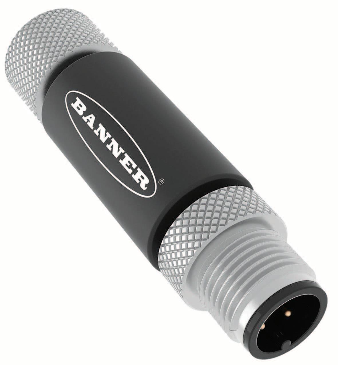
In addition to a controller and data converters, designers need wiring adapters and noise filters to quickly deploy flexible and cost-effective overlay networks. Inline wiring adapters, such as Banner’s S15A-F14325-M14325-Q, connect directly to a sensor, indicator, or other device to redirect wiring and isolate signals as needed to match specific application needs (Figure 5).
Electronica Azi International | 3/2022 20 Industry 4.0
Figure 3
©BannerEngineering
The S15C series in-line data converters can convert various types of signals including discrete, analog, and others to industrial protocols like Modbus, IO-Link, PWM and PFM.
Figure 4
© Banner Engineering
These wiring adapters are available in standard and custom configurations.
DESIGN SOLUTIONS » Modular Overlay Network
Steps in the design of a Snap Signal network include:
• Using Banner’s system diagram approach to identify and select the Snap Signal components needed for a specific installation.
• Plan the optimal wiring path, including the placement of T-connectors and filters between the devices to be monitored and the DXMR90 controller.
• Determine if the installation will require the use of a wired Ethernet connection for local data consumption or the use of an edge gateway device to wirelessly connect to a cloud platform.
S15A adapters such as the
use an
connection for easy installation and can reroute wiring as needed to match specific application requirements.
S15F in-line filters like the S15F-L-4000-Q are also important elements in an overlay network (Figure 6). They can easily solve challenges with electrical noise and transient voltages that can negatively affect network performance.
S15F in-line filters like the S15F-L-4000-Q can be readily used to protect devices from electrical noise and transients, and their M12 connection makes for easy installation wherever needed in the network
Like the S15A adapters and S15C converters, these filters have M12 connections and are packaged in an over-molded configuration that meets IP65, IP67, and IP68 standards. Installation of an S15F inline filter can result in improved signal integrity and less need for network troubleshooting.
Snap signal network design and deployment
The design and deployment of a Snap Signal overlay network begins with the identification of the data sources to be monitored. It then needs to be determined if any new sensors or indicators should be added to supplement existing devices.
Snap Signal is a true overlay network and does not require the replacement of any existing hardware. The modular plugand-play Snap Signal architecture makes installation easy:
• Install any new sensors or other devices and add splitter cables to every device to be monitored to maintain the existing connection with machine controls, while also providing a second path onto the overlay network.
Conclusion
Overlay IIoT networks can support designers needs to connect legacy equipment and islands of automation into industrial networks enabling the collection of actionable data to support increased productivity across existing factories.
The design and implementation of such an overlay network is complex, but as shown, it can be greatly simplified using Banner Engineering’s topology and Snap Signal line. The line includes the DXMR90 industrial controller, data converters, wiring adapters, filters and other elements needed to implement an IIoT overlay network and distribute it to edge computing resources or to the cloud.
The programmable, modular, and flexible design of the Snap Signal network architecture supports the addition of new devices and future proofs the installation.
Recommended Reading
■ IoT Security Fundamentals − Part 5: Connecting Securely to IoT Cloud Services
■ S15C In-Line Converters
(Converting condition monitoring and process sensors to enable OEE initiatives just got easier with Banner Engineering's S15C series in-line converters.).
■ DXMR90 Controller
(Banner Engineering's DXMR90 contains four individual Modbus masters allowing for concurrent communication to up to four independent networks.)

• Install the appropriate in-line signal converters.
• Add T-connectors, filters and other network wiring as needed to complete the network and connect to the DXMR90 controller.
• Program the DXMR90 to create custom sensing and control sequences using ScriptBasic or MicroPython programming and/or the embedded action rules.
• Connect the DXMR90 to edge computing resources using the Ethernet connection, or for cloud connections, a cellular-enabled DXM controller.
■ Digi-Key Electronics www.digikey.com

https://international.electronica-azi.ro 21
Figure 6
© Banner Engineering
S15AF14325-M14325-Q
M12
Figure 5
© Banner Engineering
Banner Engineering DXMR90 Controller Datasheet Preview

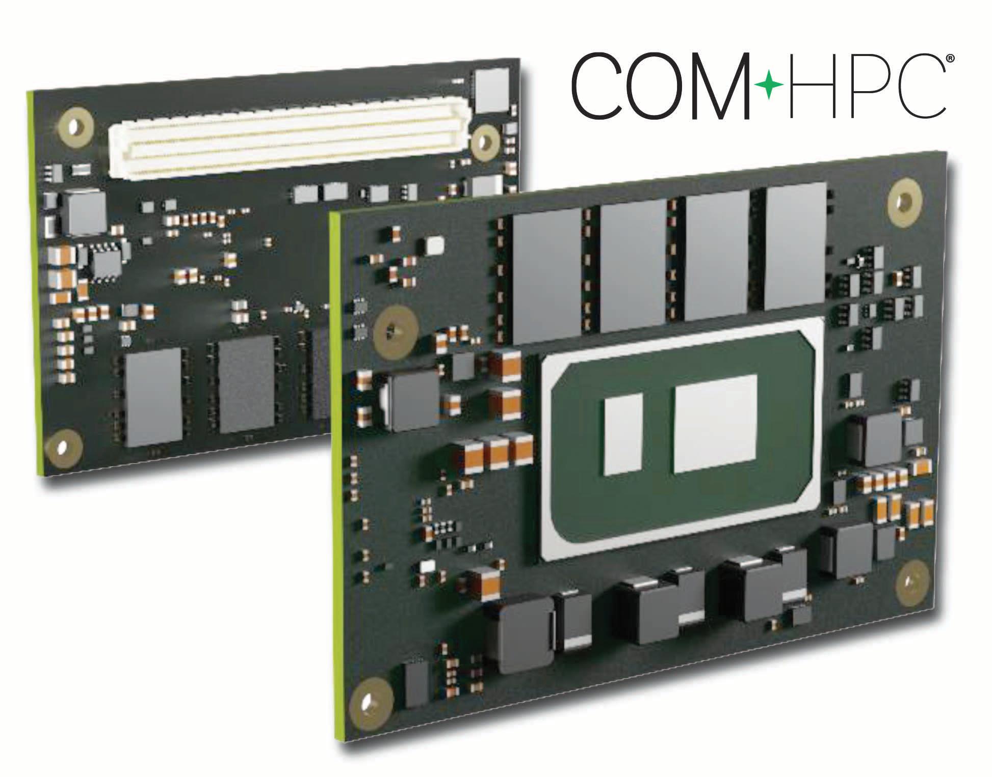
Ready for take-off
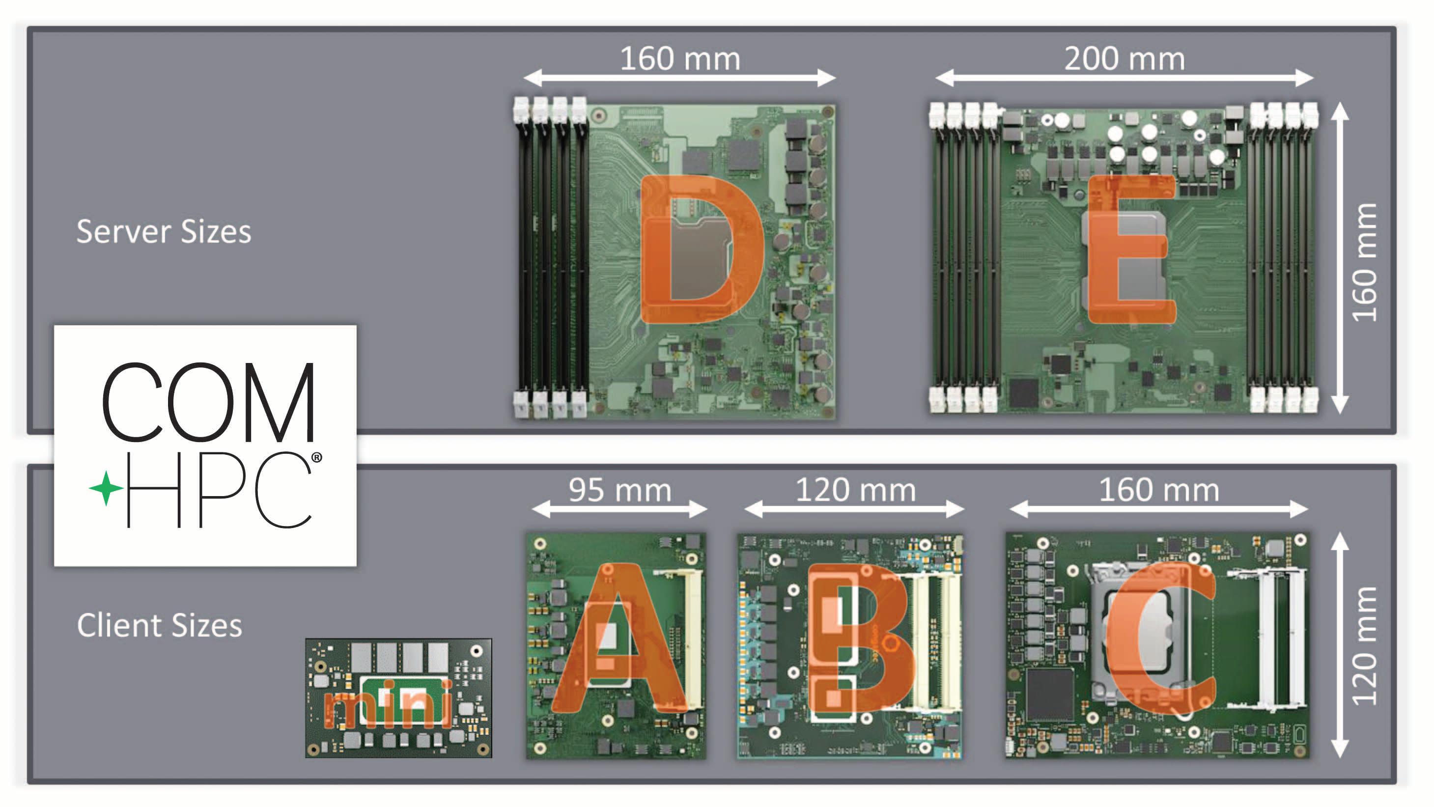
The third generation of credit card modules is coming: Despite measuring just 95×60 mm, COM-HPC client modules in Mini format will offer a comprehensive set of interfaces, including 16x PCIe, 3x graphics and several USB4 interfaces.
The third generation of credit-card-sized modules
The launch of the COM-HPC Mini form factor marks the beginning of a new era for space-saving embedded computer designs based on credit-card-sized Computer-on-Modules. This third generation will offer developers a massive performance boost and more interfaces than ever before.
Author: Zeljko Loncaric | Marketing engineer congatec


A look at the evolution of credit-card-sized Computer-on-Modules (COMs) shows that the market could well produce further variants. The first generation of such standardized modules – the DIMM PC – was replaced by COM Express Mini, to be followed by Qseven and then SMARC somewhat later. These two alternatives to COM Express Mini were created to save costs on the connector, which seemed important for low-cost, low-power processor implementations with a power consumption of
a few watts. Another reason was the ambition to serve ARM processors, which was not possible with COM Express.
In contrast, COM-HPC Mini targets the high-performance area of credit-cardsized COMs and is likely to be the only real choice for this segment.
COM-HPC Mini is also an alternative for migrating larger COM Express Compact (95×95 mm) and COM Express Basic (95×125 mm) solutions towards credit card modules. This is especially true in the

high-volume low- to mid-end segment of this form factor – as long as the processor fits the form factor.
For such designs, COM-HPC Mini offers huge space-saving potential without loss of performance and virtually no loss of interfaces. COM-HPC Mini can significantly accelerate the miniaturization trend in this segment, which – as a look at the history of credit-card-sized COMs reveals – has seen an immense increase in performance and interface density.
https://international.electronica-azi.ro 23
© congatec
DIMM PCs were the first credit-card-sized modules
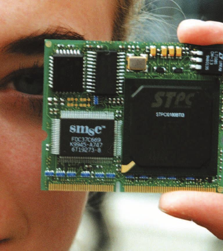
One of the pioneers in the Computer-onModule market was Hans Mühlbauer, who was involved in the activities of COM specialist congatec for a long time. Back in the early 1990s, he and his then company JUMPtec introduced the first modules based on the then common AT/ISA96 bus, which were equipped with 9.54MHz Intel CPU 80C88, offered 640kByte DRAM memory and provided an edge card connector with 120 signal and power lines on the 100×160 mm form factor.
Targeting all small and energy-efficient applications

He was also the one who developed the DIMM-PC module specification at the turn of the millennium, which was about the size of a credit card at 68x40 mm and whose edge card connector offered 144 pins. These DIMM PCs were significantly more compact than the first ModulAT COMs, yet offered more interfaces –despite the smaller footprint.
So, DIMM PCs marked the beginning of the first era of credit-card-sized COMs. This form factor was very easy to market: In 2000, for example, a variant of this specification was celebrated as the world's smallest industrial PC to date.
Admittedly, the module – called Little Donkey – was somewhat larger than the DIMM-PC specification (68×55 mm) allowed. But that is exactly why this little workhorse was also able to implement graphics, thereby for the first time offering all the functions needed for an industrial PC. Previous DIMM PCs did not support graphics.
The heart of the DIMM PC was a 100 MHz x86-compatible STPC. The main targets were small devices designed for mobile data acquisition and deployed, for instance, in rail and train systems or in operator terminals for presence and access control. These PCs were also recommended for use in vending machines and kiosk systems. In an Internet server design, the intention at the time was to implement decentralized processes for remote visualization, maintenance, monitoring and control. So in principle, there was already talk of IoT, Industry 4.0 and 5G at that time; it’s just that those buzzwords did not yet exist. In effect, everything that needed to be small, low-power and mobile could be implemented with it. The performance of those DIMM PCs and the number of provided interfaces, however, were a far stretch from what the embedded world has to offer today. Besides featuring 32 MByte DRAM and 512 kB 8-bit Flash BIOS, they had an ISA and PCI bus on board, whereby the latter was described as modern. IDE hard disks and floppy drives were still the common storage media of the day. A parallel LPT printer and two serial interfaces were also available, in addition to a PS/2 mouse and PC/AT keyboard. Because of the many parallel interfaces, there was room for just a few more I/O interfaces before the 144-pin DIMM-PC connector was fully utilized.
The connector used at that time – nomen est omen – was the one that had been specified in 1999 for SO-DIMM memory modules.
With no space left, the graphics had to be executed via an additional connector.

Computer-on-Modules take off from 2000
COMs established themselves as the most important design principle for embedded computer systems over the following years. This is especially true for the midand high-end performance class of ETX, COM Express, COM-HPC and credit-cardsized modules. Studies such as those by IHS Markit estimate that Computer-onModules accounted for around 38% of the total sales of embedded computing boards, modules and systems in 2020.
One of the main arguments for the use of modules was not having to accommodate all functions on a monolithic board as a way to cushion the rapid innovation cycles of CPUs. At that time, Intel and AMD brought new CPUs to market every 6 months. So, modules were critical for industry to ensure the required longevity of designs as it was not certain how long the older CPUs would be available. Of course, this scalability is also interesting for creating several performance variants. The argument of making the I/O board design less complex is also very important. As a rule, significantly fewer layers are required for the I/Os.
From μQseven to COM-HPC, pin count and dimensions are growing. Yet all shown form factors are roughly the size of a credit card (85,6×53,98 mm).

Electronica Azi International | 3/2022 24 COMPUTER-ON-MODULES
© SAMS Network
Eye candy: Launched in 2000, the DIMM PC ‘Little Donkey’ was the first to integrate graphics and hailed at the time as the world's smallest IPC
© congatec
This lowers the cost of the PCB design. Reducing power consumption and waste heat with each new module also played a role. And ultimately, customers then as now always want the latest CPU. This is also easy to achieve with modules.
With success, if you look at the further developments until today. A valid argument for modules was also provided by the SBC form factor PC/104, which offered not enough space for connectors when assembled on the same side as the CPU and chipset.

I/Os to the housing via an applicationspecific carrier board without any cables. These arguments apply to all module standards, regardless of performance class, and hence also to credit-card-sized modules.

Modules can also combat cable clutter
The first modules came onto the market when the use of x86 technology was still in its infancy. At that time, x86 and Windows were not yet established in industry and they were still fighting against the blue screen. In this respect, these modules were more like first 'pirate' products of a new startup industry and not representatives of the separate product lifecycle of an entire and established module standard generation. However, the company JUMPtec had already disclosed a specification at that time and was in effect doing the necessary pioneering work for the global module business.
When customer requests for more connectivity became loud, the connectors were custom-mounted on the opposite side of the PCB as well to make it possible to connect even more peripherals.
The PC/104 design principle of the time also meant that the I/Os had to be routed to the housing with cables. The resulting cable clutter led to greater susceptibility to system errors, which meant that clean and tidy cabling was what characterized a good system design at that time.
An important argument for the module concept therefore was to contain the cable clutter by connecting the external
Tough fight for the best module concept
However, the DIMM-PC form factor for these ISA/PCI-based credit card modules was not an easy success. The reason was not that there were too many alternatives, as was the case in the mid- and high-performance range, where several module concepts competed for a time until ETX finally prevailed.
The challenge with credit-card-sized modules was rather their dimensions, which were no longer suited to newer x86 processors and chipsets. The Pentium M introduced in 2003 – a revolution for the embedded market of the time – simply did not fit on a credit card.
https://international.electronica-azi.ro 25 DESIGN SOLUTIONS » The third generation of credit-card-sized modules
©
congatec
©congatec
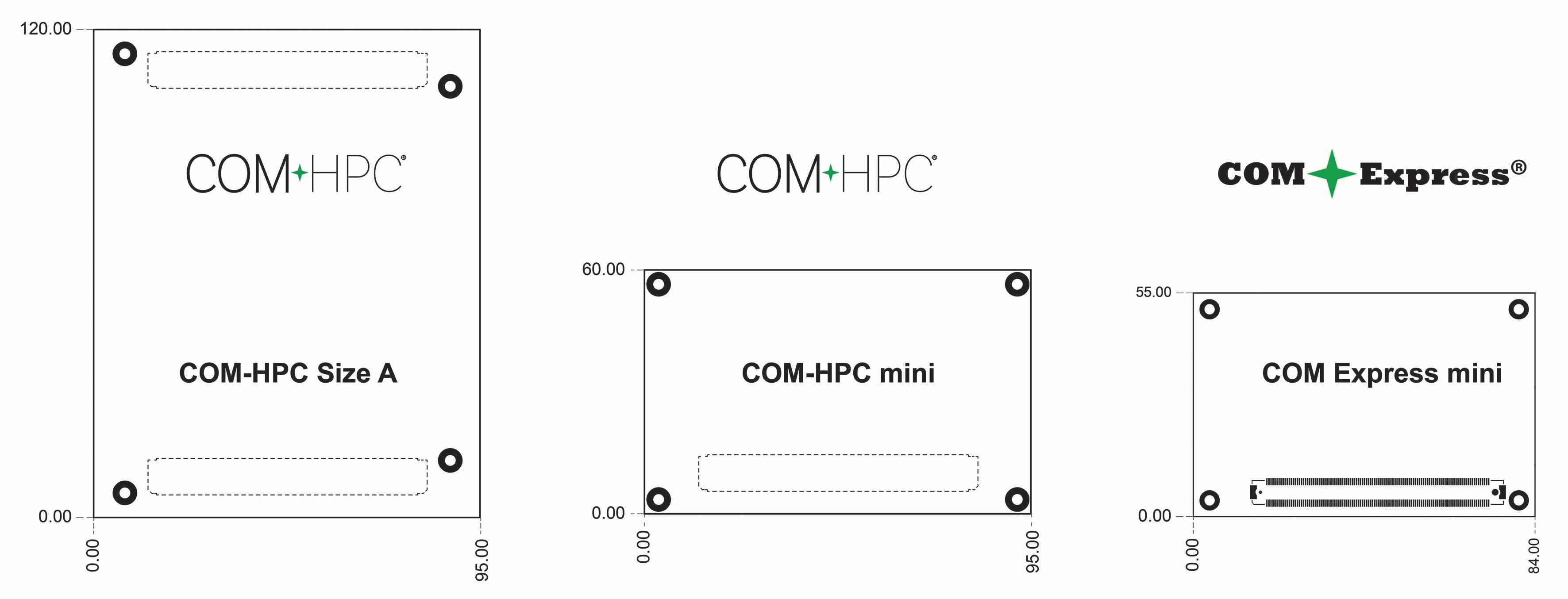
A direct comparison of COM-HPC Mini and COM Express Mini with the larger COM-HPC Size A.
First prototypes of Intel Atom processor based COM-HPC Mini modules and matching carrier boards are already in development.
For this reason, only lower-power processors could ever be used on DIMM PCs, such as the 568 ZFx86 from ZF Micro Devices, with a clock speed of 128MHz, or the STPC Elite from STMicroelectronics.
COM Express Mini
With the widespread adoption of the PCI Express bus and the end of ISA support, a new module specification was soon called for: COM Express. Officially adopted by the PICMG standardization committee in 2005, the standardization process took a good year and a half from the first presentation of the concept together with Intel in the fall of 2003. From Rev 2.0 in 2010 to the current Rev. 3.0, the COM Express specification was continuously developed under the leadership of draft editor Christian Eder, who also worked under Mühlbauer at JUMPtec, later at Kontron and then at congatec.
COM Express Mini modules took off with the launch of the first Intel Atom processors in 2008, which were the first to offer an all-in-one system controller, i.e., they combined the north and south bridge.
As a result, they fit perfectly on COM Express Mini and even today – 17 years after the PICMG launch – they are the dominant processors in this size, although there are also suppliers with AMD Ryzen or even 8th generation Intel Core processors.
The portfolio of modules available from congatec today, for example, ranges from the third Intel Atom generation through the fourth and fifth to the current Intel Atom x6000E Series processors as well as Intel Celeron and Pentium N & J processors (codename Elkhart Lake).

A second reason was the wish to cut costs. With COM Express, both the carrier and the module itself must host a connector. SMARC and μQseven, on the other hand, only require one edge card connector. Both standards use the connector developed for MXM graphics cards, which is used in notebooks. So in a way, the DIMM-PC design principle of deriving connector standards from the IT sector lives on here.
SMARC, with its 314 pins, has been the most successful among this type of credit card formats. In comparison, μQseven has only 230 pins. The number of pins could be a reason why SMARC dominates the market for credit card modules, outnumbering COM Express Mini even though over all, COM Express is the dominant form factor with all its different sizes and pinouts for client and server modules. SMARC certainly also serves a broader range of processors than COM Express Mini.
With regards to Intel and AMD processor technology, it is therefore impossible to conclude from generally available study data which standard is ultimately the leader. Fact is, however, that SMARC offers 43% more pins than COM Express Mini and 37% more than μQseven. Nevertheless, μQseven is not in decline. On the contrary: Its bigger brother Qseven is predicted to grow the most between 2022 and 2026, which will surely rub off on μQseven. Obviously, the low-end segment with fewer functions is also prospering because of the IoT trend.
The only constant is change
In addition to the very successful COM Express Basic (125x95 mm) and COM Express Compact format (95x95 mm), a COM Express Mini (84x55 mm) form factor for credit card modules was also specified. For the first time, there was now a specification for all common sizes. This uniform ecosystem encouraged leading automation suppliers worldwide to base their DIN rail PC and compact controller designs, where space is at a premium, on this specification, as it meant that they could use the same standard for all the solutions in their portfolio – with the added benefits of uniform design guides and components.
SMARC overtakes COM Express Mini
In addition to COM Express Mini, two further specifications were developed: SMARC (82x50 mm) and μQseven (70x40 mm). They are now hosted as vendorindependent standards by the second standardization body for embedded computer technology, which was founded in 2012.
A trigger for the development of these specifications was the desire to also integrate the ARM processors that were becoming increasingly popular alongside x86 technology. This, however, was not possible with COM Express Mini.
Just like elsewhere, technological progress is continuous in the world of modules, which is why it was time for the third generation of credit-card-sized Computer-on-Modules to be rung in. Presented at embedded world 2022, the new COM-HPC Mini specification aims to enable new applications in mini format that need higher performance levels than the current COM Express Mini supports. The PICMG workgroup for COM-HPC was somewhat reluctant to develop these new credit card standards as all their hands and eyes were focused on the new high-end server and client modules. But with the launch of COM-HPC, COM Express Mini users also began to wonder whether there might be a next generation of modules for them as well.
COMPUTER-ON-MODULES Electronica Azi International | 3/2022 26
© congatec
The COM-HPC ecosystem collectively describes the third generation of all Computer-onModules and provides the current high-end in each of its form factors, for which there are no alternatives in other standards today.
Inquiries are not only coming from COM Express Mini users, though, but also from the COM Express Compact group – precisely because the miniaturization of existing systems can be implemented in this way.
What does COM-HPC Mini offer?
COM-HPC Mini will offer many interfaces that COM Express cannot cover, such as USB 3.2 with 20 Gbit/s, USB 4.0 with 40 Gbit/s, PCIe Gen4/5 with up to 16 lanes, NVMe and much more. The new connector is essential for this new specification. The current COM Express connector is limited to PCIe Gen 3.0 with a clock rate of 5.0 GHz and 8 Gbit/s. The new connector supports transfer rates of more than 32 Gbit/s, enough to support PCIe Gen 5.0 or even Gen 6.0. In addition, the new processor generations for edge computing need more interfaces than before.
COM-HPC Mini will address this by providing 400 pins to the carrier board – that’s a staggering 81% more than COM Express Mini. Compared to SMARC, it is still an increase of 27%. Compared to COM Express Basic or Compact, which both offer
440 pins, 90% of the capacity of fullfledged Type 6 client modules or headless edge server modules (Type 7) is available. Anyone who doesn’t need all 100% of capacity can consequently switch.
Developers of system designs based on any of these existing form factors are now faced with the decision of whether they want to switch to the new COM-HPC Mini form factor for the next generation of their systems. However, COM-HPC Mini should not be understood as a replacement for COM Express Mini or SMARC. And just like COM Express did not replace ETX, so COM-HPC will not replace COM Express either. It is standard practice to continue to support existing designs for a long time.
To this day, there are still ETX/XTX modules that customers can deploy on the basis of the design principles of the time. In this respect, the new COM-HPC Mini module standard also proves that the basic ideas that applied back then still apply today – only at a different performance level. Of course, the tasks involved in the design-in of new processors have also become considerably more complex.
That’s why it makes much greater sense today to decouple the I/Os from the processor module by using an application-specific carrier board instead of integrating all components on a single PCB.
When will COM-HPC Mini modules become available?
The development departments of companies such as congatec are already working at full speed to define the details of the specification in the PICMG workgroup. They are also scrutinizing the first COM-HPC Mini design studies based on the latest processor technology, which semiconductor manufacturers such as Intel are sharing with them via early access programs.
The first COM-HPC Mini modules from congatec could be revealed as early as the first half of 2023. So, now is the time to evaluate COM-HPC Mini when initiating new designs.
There is no need for developers to worry whether there might also be a new generation of SMARC in the pipeline, by the way. There is currently no edge card connector that also offers 400 pins and the throughput that comes with them.
Theoretically, the OSM standard could be an alternative; but as this specifies solderable modules, it is hardly comparable with pluggable modules. OSM Size-M (medium) offers 476 pins on 30×45 mm while Size-L (large) measures 45×45 mm and impresses with 662 BGA pins. However, high-performance processors are too big for this format, so it will be some time before such solutions are ready for the Intel Atom processor class.
The bottom line is that there is basically no way around COM-HPC Mini. For developers, this means above all the greatest possible design security.
ETX, COM Express and COM-HPC
Besides the market for credit-card-sized Computer-on-Modules, there is also the market for mid- and high-performance computer modules. ETX and COM Express are two Computer-on-Module form factors that were defined by independent standardization bodies for this sector, establishing themselves and providing ever more performance at significantly higher levels in the course of technological progress.
With COM-HPC, a third generation was launched in 2019 to serve the highest performance demands of broadband and 5G-connected devices, machines and systems. Like COM Express, it offers server as well as client modules. The credit-card-sized modules round out the offering of both specifications
■ congatec www.congatec.com
https://international.electronica-azi.ro 27
DESIGN SOLUTIONS » The third generation of credit-card-sized modules
Maximizing Power Density
As the world strives for carbon neutrality, electric vehicles (EVs) are rapidly taking market share from internal combustion engine vehicles. However, one of the issues with electrics vehicles is range anxiety, as customers are unsure of how long they will be able to drive without the car needing to be charged. To combat this, governments around the world are massively investing in charging infrastructure.
Several types of charging stations are being used today, from Mode2 and Mode3 charging stations to Mode4 DC fast-charging stations that can provide up to 400kW of power (see Figure 1). These charging stations are described in greater detail below.
• Mode2 and Mode3 (Active cables with IC-CPD and Wallboxes) These stations provide AC power to charge an electrical vehicle.
(Note: Mode 1 is no longer valid in Europe). Using 3 phases Mode 2 allows to charge an EV with up to 22kW while Mode 3 allows up to 42kW (~75 km range per hour of charging).
• Mode4 (DC fast chargers (DCFC) This charging stations can charge an EV battery from 20% to 80% within 30 minutes, depending on the power rating (50kW to 400kW) of the charging station itself and the maximum power that the vehicle can be charged at.


When charging at home or at work, Mode2 and Mode3 stations are sufficient. However, Mode4 and supercharger stations are necessary for people who cannot charge over longer periods of time, such as when a driver is on a longer trip where the battery’s full capacity is utilized.

Figure 2 shows a typical DC fast-charging station block diagram to convert a 3phase AC voltage into a 250V to 800V DC voltage to charge electric vehicles.
A Mode4 station typically contains several of these subunits, each ranging from 30kW to 75kW. This diagram exhibits many of the solutions that can drive DC fast charging stations, including isolated gate drivers, isolated power modules, transformer driver bias, and digital isolator solutions with an integrated power supply.
Figure 2 shows that the DC Fast charger system is generally comprised of two conversion stages. The first stage is a power factor correction (PFC) stage, which converts the AC voltage from the power grid into an intermediate DC voltage bus between 800V and 1300V.
Three-phase, 3-level rectifier/inverter topology is commonly used for the PFC stage. This particular topology refers to a three-level converter that can interface with a 3-phase power grid.
At the second stage (also called the DC/DC stage), an isolated DC/DC converter converts the intermediate DC voltage to the
Electronica Azi International | 3/2022 28
With an innovative 5MHz LLC transformer driver
Figure 1: Electric Car Charging Stations.
©AdobeStock/Mike Mareen
POWER
©AdobeStock/Blue Planet Studio
target voltage that is specific to the battery being charged. LLC and phase-shift fullbridge converters are common topology choices for the DC/DC stage.
Some of the challenges for designing highpower charging stations are maximizing power density, reducing cost, and reducing size. One industry-wide method to increase efficiency is to replace semiconductor MOSFETs/IGBTs with silicon carbide (SiC) FETs. This is particularly important since DC Fast charger stations have increased in power from 50kW up to 400kW.
Due to the high-voltage and high-power nature of DC Fast charger systems, isolated devices are required to protect users and low-voltage control circuitry from the potential hazards and disturbances that could originate from the high-voltage power conversion circuits. Additional components can be implemented to reduce the risk of hazards:
• Isolated gate drivers for SiC MOSFETs and IGBTs, such as the MP18831 and MP18851
• Digital signal isolators, such as the MPQ27811 and MP27631
• Isolated current-sensing and voltagesensing devices, such as the MCS1806 and MCS1803
Note that isolated gate drivers require an isolated bias supply for power, and that the gate drive power supplies must be able to withstand high isolation voltages.

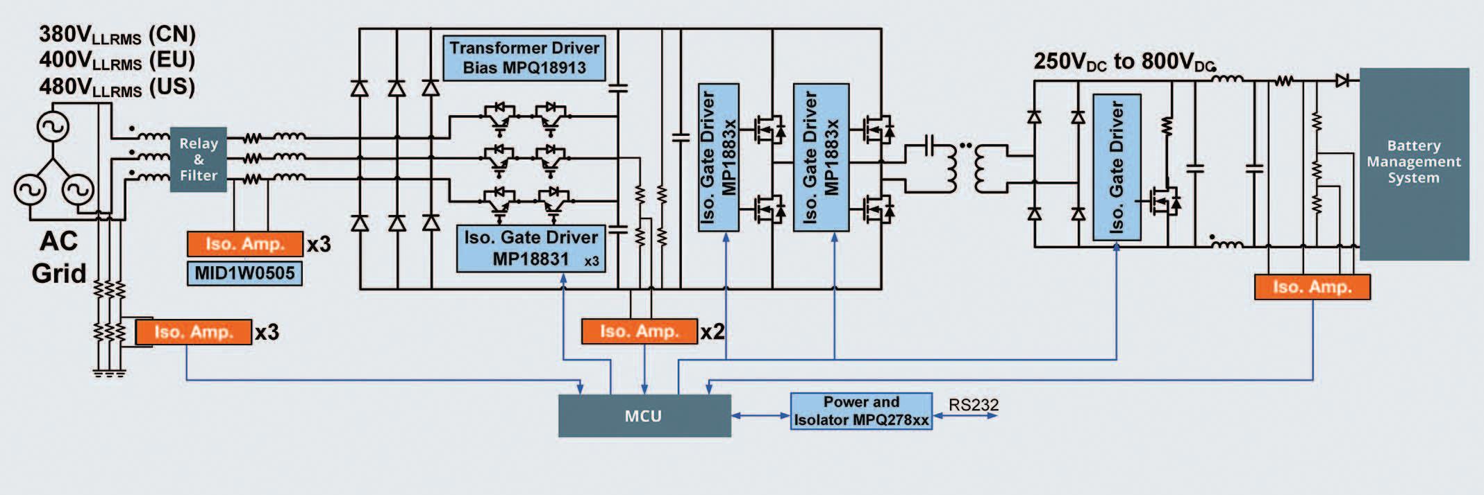
At minimum, the gate driver power supplies must be able to withstand the intermediate DC bus voltage, and must offer low isolation capacitance to minimize disturbances from the high-voltage side to the low-voltage side.
Designing an isolated power supply for gate drivers
The MPQ18913 is a transformer driver for isolated bias supplies. This device can work with SiC FETs as an isolated bias for SiC gate drivers. Flyback topology is often used for isolated power supplies to provide an isolated 18V/-4V output that drives the SiC FET. Figure 3 shows a typical application circuit implemented with the MPQ18913 to achieve a 18V/-4V output.
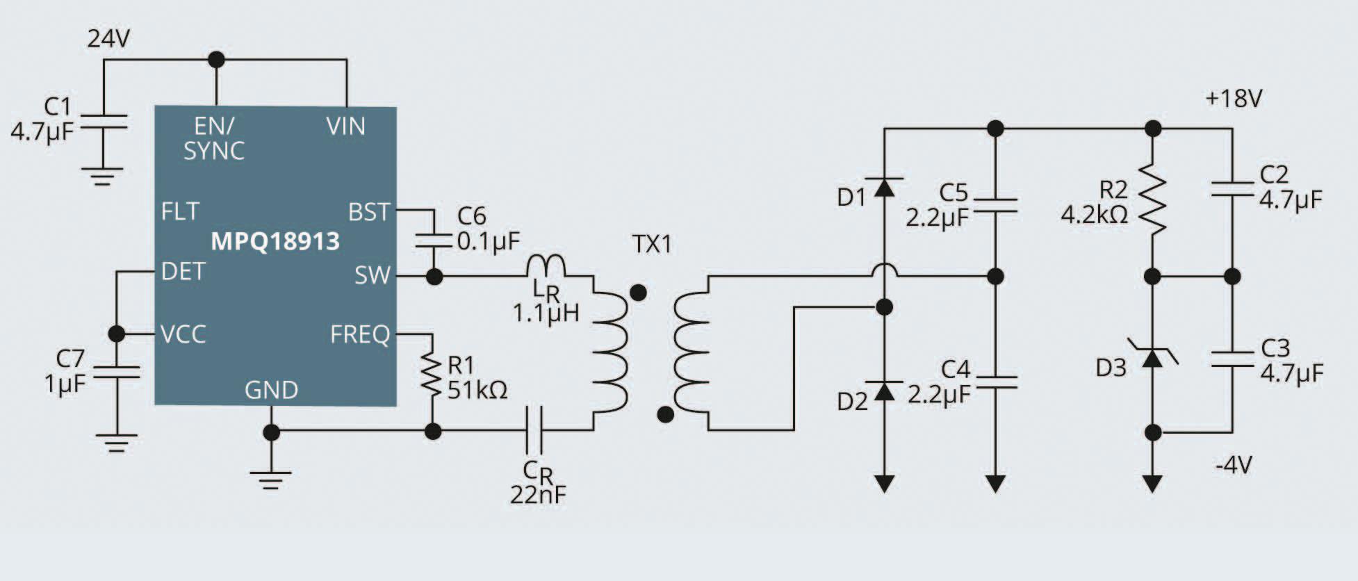
The number of outputs can be configured based on the transformer used and the output voltage can be altered via the turns ratio.
The MPQ18913 can be used as an LLC converter, which is the most efficient topology for isolated gate drive power supplies (see Figure 4). These converters use a resonant LLC tank, which has a magnetizing inductor for energy transfer, as well as an additional capacitor and inductor that make the tank resonate at a certain frequency. The converter uses this resonance to achieve soft switching and ensure highly efficient power conversion. The main benefit of LLC converters is that the leakage inductance created by the transformer can be used as the resonant inductor in the tank. This eliminates the voltage spike induced by the leakage inductance, and improves efficiency compared to flyback topologies.
https://international.electronica-azi.ro 29
©
Figure 2: Block Diagram of a Mode4/DCFC Subunit.
CODICO
Figure 3: MPQ18913 Application Circuit. © CODICO
SOLUTIONS » The
©AdobeStock/Vlad DESIGN
EV Charging Infrastructure
Using the MPQ18913 as an example, the LLC resonant topology offers several notable advantages compared to a typical PSR flyback topology.
One such advantage is that LLC resonant topology reduces the solution size due to the switching frequency (fSW), which can reach up to 10MHz, whereas with flyback topology, fSW stays below 400kHz. This results in a total solution size that is 40% smaller than a flyback application using a similar power level.
Another major advantage of LLC resonant topologies is the fact that the isolation voltage can easily reach up to 5kV. Traditional flyback solutions only reach 1.5kV, therefore meeting more stringent isolation voltage requirements.
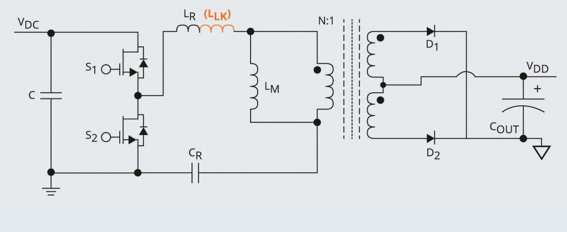
Table 1 compares LLC resonant topology to flyback topology.
Conclusion
High-frequency LLC power supplies are typically more difficult to implement and optimize in designs than low-frequency
converters, but devices like the MPQ18913 simplify LLC power supplies with features including automatic resonant frequency detection and integrated transistors.
In addition, LLC resonant topologies reduce solution size, which increases power density for high-power charging stations such as those used for charging electric vehicles.

As electric charging infrastructure continues to improve the MPQ18913, being used to bias SiC FETs, is a perfect choice
in high-power charging applications, as well as in automotive applications such as on-board chargers, traction inverters, and DC/DC converters.
Contact:
Gabor Lefanti
Field Sales Engineer

Matroz Str. 4/b, 1213 Budapest, Hungary
Mobile: +43 1 86305-272
■ CODICO www.codico.com
Electronica Azi International | 3/2022 30
© CODICO
Figure 4: LLC Topology.
POWER Parameter LLC Resonant Topology PSR Flyback Topology Benefit Switching frequency (fSW) High (up to 10MHz) Low (<400kHz) Transformer size 13μH (11mm × 6mm) 30μH (10mm × 10mm) Leakage inductance Utilizes leakage Leakage inductance In LLC, leakage inductance inductance as part reduces performance enables higher efficiency of the resonant tank and prevents voltage spikes Isolation voltage High (up to 5kV) Low (1.5kV) LLC enables higher isolation voltage to increase safety Isolation capacitance Low (6pF) High (Up to 25pF) Package size 2mm × 2.5mm 4mm × 4mm Diodes (including Zener diode) 3 6 Solution size 109mm2 180mm2 BOM components 21 components 26 components Table 1: LLC Resonant Topology vs. Flyback Topology Up to 40% reduction in solution size and 20% fewer component count High frequency enables much smaller solution size ©AdobeStock/kinwun

Multiturn Position Sensor Provides TPO Capabilities (True Power-On) with Zero Power
This article outlines the current methods used to enable true power-on (TPO) multiturn sensing capabilities and introduces a new simplified solution that is set to reshape both the industrial and automotive position sensing markets.
The simplified system will enable designers, with or without magnetic system design experience, to replace bulky and expensive incumbent solutions.
Authors: Stephen Bradshaw | Product Applications Engineer
Christian Nau | Product Marketing Manager
Enda Nicholl | Strategic Marketing Manager Analog Devices
Introduction
Position sensors and encoders are ubiquitous in automotive and industrial applications where it is vital that the position of the system is known at all times. However, incumbent position sensors and encoders can only provide a single turn or 360° TPO position information. Systems that require TPO position information over multiple rotations or wider measurement range typically incorporate a backup power supply to track and memorize the multiple rotations of the single turn sensor after an unexpected loss of power, or to track multiple turn movement during key-off or powerdown. Alternatively, a gear reduction mechanism can be added to the system to reduce the multiple rotations to a single turn, and in combination with a single turn sensor, to find TPO multiturn position information. These solutions are expensive and bulky, and, in the case of the battery backup system, a regular maintenance contract is required. Rotary and linear encoders are key devices used in applications where the system designer needs to ensure that the
position of a mechanical system is always known for closed-loop control, even after a loss of power either as part of the normal operating cycle or accidental. The challenge for system designers is to ensure that the TPO position is available even after a loss of power. If the system state is lost, then a lengthy and often complex procedure is required to reset the system into a known state.
Incumbent Solutions
Modern factories are becoming more dependent on robots and cobots to reduce cycle times, increase factory throughput, and improve efficiency. One of the major costs and inefficiencies associated with standard robots, cobots, and other automated assembly equipment is the resulting downtime required for rehoming and intializing power-up following a sudden loss of power while operating. This resulting downtime and productivity loss are both costly and inefficient. Although this issue can be solved with backup batteries, memory, and single turn sensors, these solutions have their limitations.
Battery packs have a limited life span, and maintenance/service contracts are required to manage the battery replacement. In certain environments, where there is a risk of explosion, the maximum energy that can be stored in the battery pack is limited. The reduction in energy storage leads to a shorter maintenance cycle where the batteries must be replaced more frequently.
An alternative to battery backup is the use of Wiegand wire energy harvesting modules. These modules make use of a specially treated wire where the magnetic coercivity of the outer shell is much higher than the coercivity of the inner core. The different coercivities create voltage spikes at the device output when a magnetic field is rotated.
The spikes can be used to power external circuitry and record the number of turns in a ferroelectric random-access memory (FRAM). The magnetic multiturn memory that has been developed by Analog Devices requires no external power to record the number of rotations of an external magnetic field. This leads to a reduced system size and cost.
Electronica Azi International | 3/2022 32
INDUSTRIAL CONTROL
Multiturn Sensor Technology
At the core of the magnetic multiturn sensor is a spiral of giant magnetoresistance (GMR) material made up of multiple nanowires of GMR elements. The operating principle of the sensor is based on shape anisotropy and the generation of domain walls in a domain wall generator in the presence of an external magnetic field. As the external magnetic field rotates, the domain walls propagate through the narrow spiral tracks (nanowires) attached to the domain wall generator, as shown in Figure 1.
power-on (TPO) multiturn sensing capabilities
When power is reapplied to the sensor, a reading of the turn count state is available with no further user actions or system resetting required.
A combined technology solution that simplifies system design
The top level block diagram of the ADMT 4000, shown in Figure 2, combines the earlier described GMR multiturn sensor with a highly accurate AMR angle sensor and integrated signal conditioning IC to provide a solution that is capable of recording 46 turns or 16,560° of movement with a
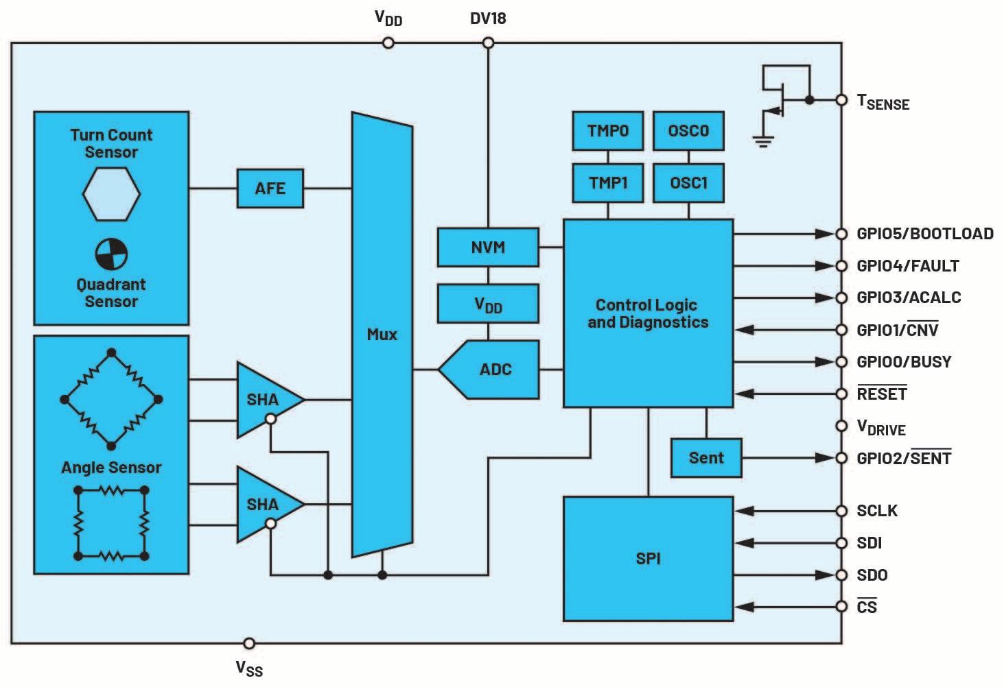
ADI is preparing a magnetic reference design that will enable users with little or no magnetic design capability to easily adopt the ADMT4000 in their application. In addition to the core magnet design, this reference design will also provide immunity and robustness to stray magnetic fields, which will allow customers to implement the sensor in harsh environments.
As the domain walls move through the spiral leg structures, the state of each spiral leg element changes. Since the elements are fabricated from GMR material, the state of each one can be determined by measuring their resistance.
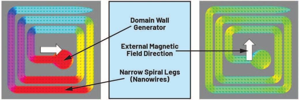
The sensor relies only on the external magnetic field, and no additional backup power or energy harvesting technique is needed for the turn counting operation.
typical accuracy of ±0.25°. The integrated signal conditioning IC enables further system enhancements to support harmonic calibration, which can remove errors due to magnetic and mechanical tolerances from the application. The ADMT4000 provides absolute 46 turn (0° to 16,560°) digital output via an SPI or SENT interface. The ADMT4000 is positioned opposite a dipole magnet mounted to the rotating shaft as depicted in Figure 3.
Stray fields can be generated from many sources where currents are carried in a wire, in particular, when used in close proximity to electric motors or actuators. ADMT4000 capabilities are valuable in many industrial applications including robot and cobot arm joint position tracking in the event of a power outage or during power-down (see Figure 4).
Other industrial applications include the absolute and TPO tracking of x-y tables in industrial automation, machine tools or medical equipment applications (shown in Figure 5).
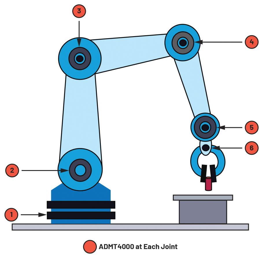
Other rotary to linear applications include, but are not limited to the turn counting of coils, drums, spools, reels, hoists, winches, and lifts (Figure 6) when powered or movement tracking when powered down or during power outages.
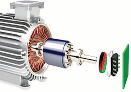
https://international.electronica-azi.ro 33
SOLUTIONS » True
DESIGN
© ADI
Figure 3: The ADMT4000 typical application assembly.
©
Figure 1: The multiturn principle of the operation.
ADI
©
Figure 2: The ADMT4000 multiturn sensor block diagram.
ADI
©
Figure 4: The ADMT4000 in a robot/cobot application.
ADI
Additionally, TPO position sensing provided by the ADMT4000 is of significant value for automotive applications including, but not limited to, transmission actuators (Figure 5), electrical power steering (EPS) including steer-by-wire (Figure 7), parking lock actuators, other general-
purpose actuators, and seat belt retractors (Figure 8). The size, cost, and operating temperature range of the ADMT4000 enable its use in a wide range of applications including safety critical applications in the automotive and industrial space.
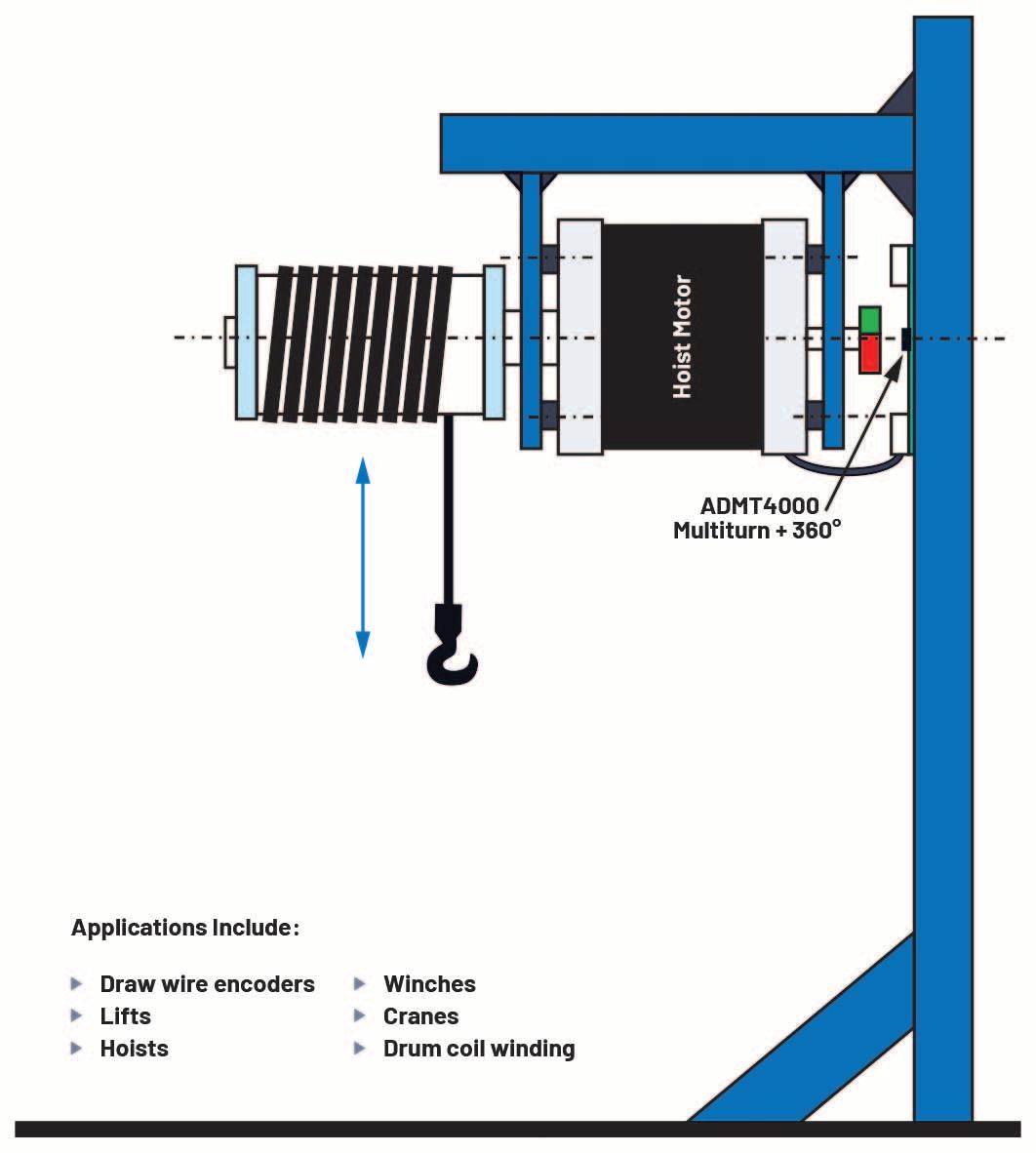
Automotive safety critical applications are compliant to the ISO 26262 standard and a particular automotive safety integrity level (ASIL). The ADMT4000 will be supplied as either ASIL-QM or ASILB(D) to suit applications that do and don’t need the advanced ASIL or SIL functionality.
Conclusion
The ADMT4000 and the first integrated TPO multiturn position sensor are set to significantly reduce system design complexity and effort, ultimately resulting in smaller, lighter, and lower cost solutions. The ease of use of the ADMT4000 will enable designers with and without magnetic design capability to add new and improved functionality to current applications and open the door to many new applications.
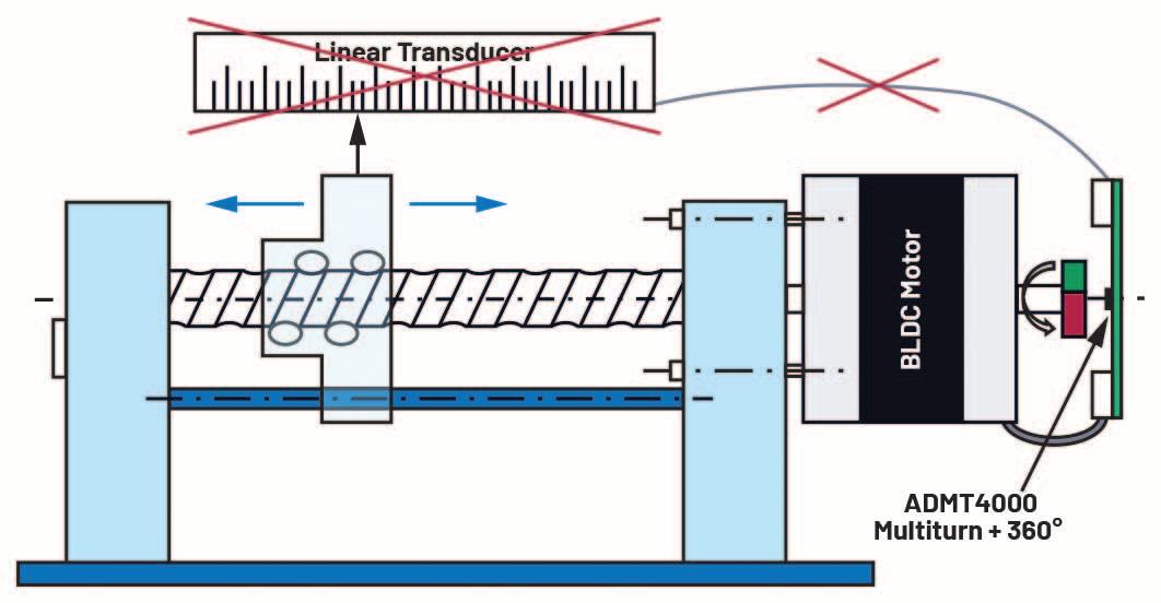
To find out more about the ADMT4000 and the magnetic reference design, please contact your local ADI sales team who will be happy to discuss your requirements and applications or visit https://www.analog.com/en/productcategory/magnetic-field-sensors.html

■ Analog Devices www.analog.com

Electronica Azi International | 3/2022 34
■ ADMT4000
© ADI
Figure 5: The ADMT4000 in a rotary to linear actuator application.
© ADI INDUSTRIAL CONTROL
Figure 6: Wire draw encoder applications.
Engage with the ADI technology experts in our online support community. Ask your tough design questions, browse FAQs, or join a conversation.
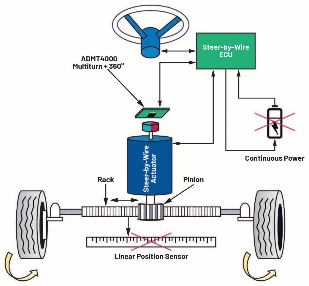
Visit: https://ez.analog.com

About the authors
Stephen Bradshaw has a B.Eng. in electrical engineering from the University of Leeds as well an M.Sc. and Ph.D. in optoelectronics from the University of Glasgow. During the early part of his career, Stephen was responsible for the design and characterization of the lens used in the first generation of mobile phone cameras with STMicroelectronics before working on Gbps optical transceivers at Maroni and most optical transceivers at Nanotech Semiconductor. Stephen has been with ADI for over 10 years as an applications engineer supporting both LiFe and Pb-Acid battery monitoring product lines and magnetic position sensors.


Christian Nau is a product marketing manager at Analog Devices and has a background in automotive electronics and sensors. He joined ADI in 2015 as a field applications engineer and subject matter expert supporting magnetic sensors in the EMEA region. Since 2019, Christian has been working in ADI’s Magnetic Sensor Technology Group, supporting customer engagements on existing products and working on the future direction of the group covering multiple markets.
Enda Nicholl is a strategic marketing manager for magnetic sensors at Analog Devices based in Limerick, Ireland. Enda was a mechanical engineer and joined ADI back in 2006. He has almost 30 years of experience in the field of sensors and sensor interface products across a broad range of applications and markets including automotive and industrial. Enda, throughout his career, has worked in product applications, field applications and sales, as well as strategic business development and marketing.

https://international.electronica-azi.ro 35
© ADI
Figure 7: A steer-by-wire application.
© ADI
Figure 8: A seat belt retractor application.
SOLUTIONS » True
DESIGN
power-on (TPO) multiturn sensing capabilities
Power to Space Farming!
At the APEC 2022 Plenary Session, John H. Scott, Principal Technologist, Power and Energy Storage, NASA Space Technology Mission Directorate presented a very interesting topic: ‘On the Moon to Stay’, covering the various aspect of the power electronics that would be required to make that statement feasible. Space exploration has not only been a dream and a source of imagination, but also an amazing research area in which to break ‘unbreakable’ limits, and provide benefits to many applications we are now using daily on planet Earth.
Author: Patrick Le Fèvre Chief Marketing and Communication Officer Powerbox (PRBX)

Taking humans to the moon, later to Mars and who knows where to next, is far from being an easy job as making life possible and sustainable in such hostile environments is much more than just ‘a challenge’. One example is how to feed the space explorers when they are so remote from Mother Earth? Considering Mars, at huge cost and risk it would take 210 days for a re-supply rocket to arrive, which is clearly not an optimum solution. Space farming has been part of that dream and we all remember the O’Neill Cylinder, designed by Princeton physicist Gerard K. O’Neill who published in 1974 an article in Physic Today: ‘The Colonization of Space’. O’Neill article and research fueled a number of sci-fi movie showing the huge rotating cylinder, hosting farms and lit by an artificial sun (figure 1).
We are not there yet but on that basis the first humans to inhabit Mars may be considered farmers rather than astronauts! So how will power electronics contribute to make the dream a reality?


From Earth indoor farming to Space FEEDING 10 BILLION PEOPLE ON EARTH
Let’s start at the beginning and if we consider the latest estimation, Earth’s population is expected to reach 10 billion by 2050. Simultaneously we are facing climate conditions changes that could affect the complete food ecosystem and require significant modification to the ways in which we produce and consume food.
Considering all the parameters and requirement to produce food with the highest respect for the environment, in 1999,
Dr. Dickson Despommier with his students developed the idea of a modern indoor farming, revitalizing the terms coined in 1915 by the American geologist Gilbert Ellis Bailey: “Vertical farming.”
We have all heard about it, read a lot of articles about industrial building converted into vertical farms but from the early days using fluorescent or halogens lighting to Solid State Lighting (SSL), there is an amazing number of technology innovations contributing to optimize the energy delivered to the plants for optimal growth and benefits of indoor farming multiples.
If we consider space utilization, 100 time more food could be produced by square meter compared to regular agriculture, reducing water utilization by 90% and hazardous chemical to none. Indoor farming are very attractive though to be really efficient such agriculture requires a very efficient lighting system (figure 2).
Electronica Azi International | 3/2022 36
Not all vegetables can grow with limited soil and nutrition by impregnation but for the ones applicable with this farming method, the results are impressive and getting even more impressive when using modern lighting technologies computercontrolled, which for power designers is a very interesting area to explore, combining advanced power electronics and modern agriculture, with software in mind. Since its introduction, indoor farming engineers conducted researches to validate spectrum and energy required by different plants to grow efficiently. From wide spectrum fluorescent or halogen lamps to more narrow spectrum, the conventional lighting industry innovated a lot but those technology not flexible nor efficient enough to respond to the demand.


Following experimentations in Japan in 2005-2008, agronomical researchers investigated the different lighting methods to adjust spectrum and energy to specific plants. Researchers concluded that the specific light spectrum to grow plants and vegetables typically starts at 450 nm (blue light) and goes through 730 nm (far red) (figure 3). The Photosynthetic Photon Flux Density (PPFD) required ranges from 50 micromoles (μmol) for mushrooms up to 2,000 micromoles for plants like tomatoes and some flowers that thrive in full summer light (figure 4).

https://international.electronica-azi.ro 37
© PRBX
Figure 4: Light energy required ranges from 50 micromoles (μmol) for mushrooms up to 2.000 micromoles for light intensive plants.
Figure 3: The light spectrum to grow plants and vegetables typically starts at 450 nm (blue light) and goes through 730 nm (far red) .
© PRBX
©
/ asharkyu-Shutterstock
Figure 2: Solid State Lighting to grow vegetables in indoor farming.
PRBX
Figure 1
O’Neill Cylinder interiorPainting by Rick Guidice.
© PRBX/NASA
Agricultural experts tell us that for optimal results different plants types may require different light spectra as well as differing light balance and intensities between the seedling to harvesting stage. This often results in a requirement for the artificial light to have a number of different spectra channels that are individually adjustable for intensity.
BRINGING EARTH FARMING TO SPACE
As NASA plans long-duration missions to the Moon and Mars, a key factor is figuring out how to feed crews during their weeks, months, and even years in space. Food for crews aboard the International Space Station (ISS) is primarily prepackaged on Earth, and requiring regular resupply deliveries.
After a series of experiments and taking into consideration the full development cycle, it was decided to grow a variety of plants including lettuces, mustard varieties, and radishes. Firstly in a controlled lab on Earth, then in the ISS to study how plants are affected by the micro-gravity and other factors (figure 6).

The ‘Veggie’ project included a large number of experimental factors e.g., “Pick-andEat Salad-Crop Productivity, Nutritional Value, and Acceptability to Supplement the ISS Food System (Veg-04A)” including research on the optimum lighting conditions to grow plants.

Some crop growing processes combine different sources of lighting, including the use of UV flashes to prevent the development of parasites, requiring a power supply able to switch from constant voltage to constant current within a range from almost zero to the maximum (figure 5).
This specification for a power supply is very much what will be required for Space Farming, with, for sure, a power electronics architecture able to combat the effects of space radiation.
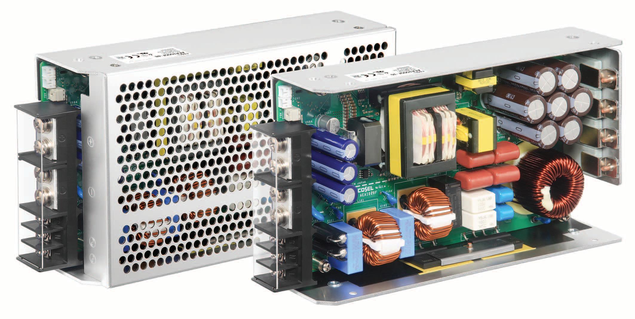
Now, while the ISS is able to be resupplied by cargo spacecraft, clearly it is much more complicated and expensive when based on Mars, which is at an average distance of 220 million km (140 million miles) and more than 200 days traveling.
In 2015, NASA in association with the Fairchild Botanical Gardens in Miami began a project called ‘Growing Beyond Earth’ to define what plants would be suitable from autonomous space-farming.
On the ISS, two light treatments with different red-to-blue ratios were tested for each set of crops to define light colors, levels, and horticultural best practices to achieve high yields of safe, nutritious leafy greens and tomatoes to supplement a space diet of pre-packaged food, and later for Moon or Mars farming.
A number of reports have been released e.g., ‘Large-Scale crop production for Moon and Mars: Current gaps and future perspectives’ published in February in ‘Frontiers in Astronomy and Space Sciences’ summarizing seven years of experimentation on Earth and in the ISS (figure 7).
Electronica Azi International | 3/2022 38 POWER SUPPLIES
Figure 6: NASA astronaut Peggy Whitson looks at the Advanced Astroculture Soybean plant growth experiment.
© PRBX/NASA
Figure 5: COSEL power supply with multi-modes for voltage or current constant from max to near zero.
© PRBX/COSEL
Figure 7
Examples of Kennedy Space Center 8KSC) prior, current and future space crop production platforms selected and designed to lead to crop production units destined for the Moon or Mars.
© PRBX/NASA
Considering the different varieties of plants to grow, the distance and cost, the power supplies for space-farming will have to accommodate different power profiles combining constant current or constant voltage, peak power, and to be energy efficient and small in size. That’s in addition to specific constraints related to space in terms of immunity to radiation, operating temperature, shock and vibration.
The importance of optimizing the payload, the weight and size of everything is a big concern for space applications, and from low orbit satellites to out-of-space exploration, power supplies have been developed with very advanced technologies to make them smaller and energy efficient.
Wide Band gap semiconductors in space applications have formed a part of many research projects, and it’s worth mentioning the report presented by NASA, in 2018, at the (RADECS) conference in Gothenburg: ‘Radiation and its Effects on Components and Systems’.
References
• Powerbox (PRBX): https://www.prbx.com/
This identified the strengths and weaknesses of WBG when exposed to radiation, and the recent announcement about the newly funded national collaboration led by Penn State to better predict and mitigate radiation-induced damage of WBG semiconductors interesting.
The U.S. Department of Defense awarded the team a five-year, $7.5 million Defense Multidisciplinary University Research Initiative Award. This clearly shows the high level of importance of WBG in space applications and their contribution to the next step.
In parallel, the semiconductor industry is moving forwards and one example is the new division and products for space applications launched by Efficient Power Conversion (EPC).
For power designers, having access to COTS ruggedized GaN for space applications will reduce the development time and cost when developing power supplies for space applications (figure 8).
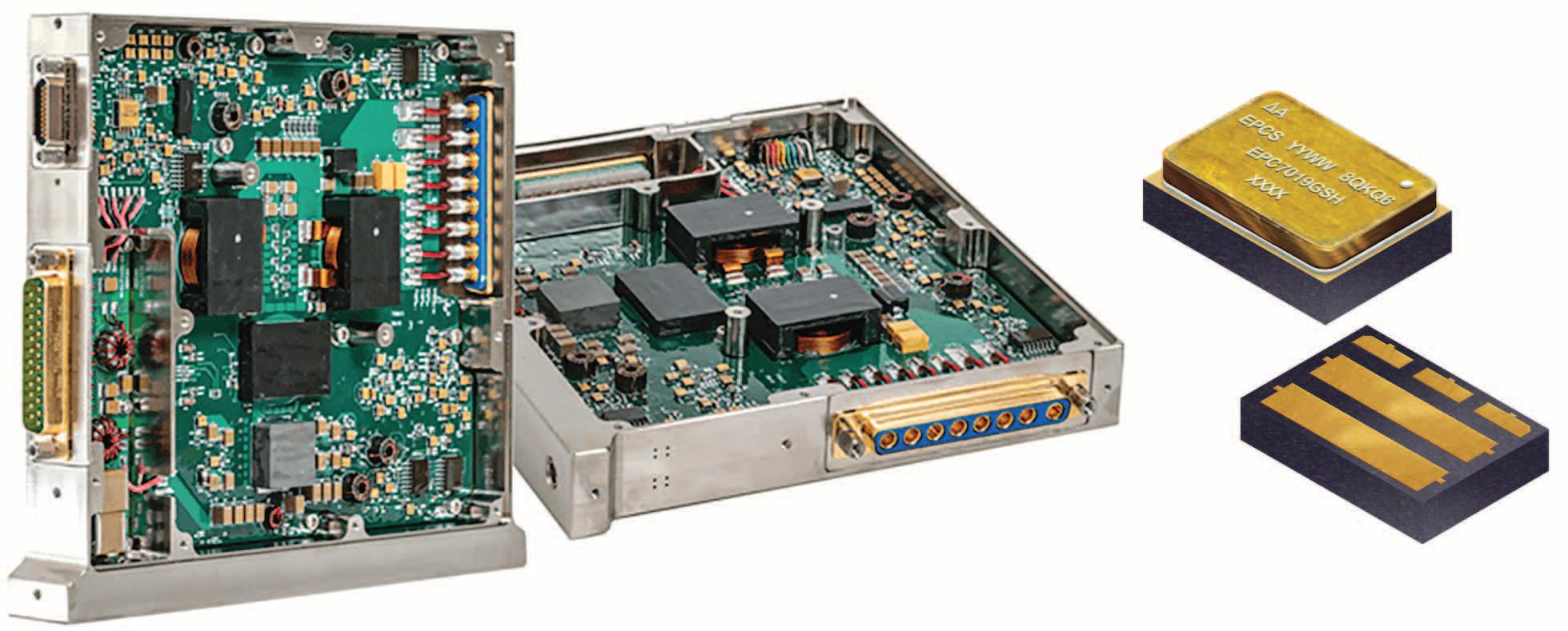
Conclusions
Although one of the biggest challenges to in-spaceship farming is sourcing enough water and nutrients and then cycling them as efficiently as possible, there are many other obstacles we don't yet fully grapple with on Earth that will have to be considered too, such as cosmic radiation, lack of an atmosphere, and low levels of light.
From the 2015 ‘Growing Beyond Earth’ project to 2022, a lot of progress has been made, contributing to a better understanding of space farming, as well as in power electronics. We are in the early stages of a whole new era in which Wide Bandgap semiconductors in power electronics will play an important role.
Exciting time for power designers, isn’t it?!
■ Powerbox (PRBX) www.prbx.com
• The Colonization of Space – Gerard K. O’Neill, Physics Today, 1974. (https://space.nss.org/the-colonization-of-space-gerard-k-o-neill-physics-today-1974/)
• Fairchild Botanical Garden: (https://fairchildgarden.org/gbe/)
• Growing Beyond Earth: (https://www.nasa.gov/feature/students-help-nasa-researchers-decide-what-plants-to-grow-in-space)
• NASA / RADEC 2018 Jean-Marie Lauenstein – NASA GSFC, Greenbelt, MD, USA. Wide-Bandgap Semiconductors in Space: Appreciating the Benefits but Understanding the Risks
• Frontiers in Astronomy and Space Science. Large-Scale Crop Production for the Moon and Mars: Current Gaps and Future Perspectives Published 04 February 2022 / doi: 10.3389/fspas.2021.733944
• Efficient Power Conversion (EPC) (https://epc-co.com/epc)
• Applied Power Electronics Conference (APEC) (https://apec-conf.org/)
https://international.electronica-azi.ro 39 DESIGN SOLUTIONS » Spaceship farming
© PRBX/EPC
Figure 8: Efficient Power Conversion (EPC) ruggedized GaN FET for space applications and DC/DC converter.
Charging into the future
Author: Joseph A. Thomsen Vice President, MCU16 Business Unit Microchip Technology

With many countries looking to ban the sale of new vehicles that use gasoline and diesel engines starting in 2030, the development of electric vehicles (EV) is set for tremendous growth. This is driving the need for more efficient and more cost effective EV designs with longer driving range and lower cost to help encourage consumers make the switch. However, the overall impact of electric vehicles (EVs) on the world is underestimated. The tendency is to think the transition is as easy as swapping gasoline tanks and engines for batteries and electric motors, but the reality is much more complex.
Emerging Technologies for Powertrain
New power MOSFET technologies are one key part of this switch-over to electric operation for EV traction inverters to support increased efficiency and higher voltages. There is a lot of talk about using new wide-bandgap (WBG) technologies such as silicon carbide (SiC) and gallium nitride (GaN) for the powertrain of electric vehicles. New SiC designs are emerging to meet the growing high-power requirements for EV.
GaN technology is growing but still needs to build confidence for proven reliability and drive lower prices in order to penetrate the EV inverter market. Both SiC and GaN are more expensive than traditional solutions, but they offer compelling features such as higher efficiency due to lower switching losses as well as
lower system size and weight, due to higher switching frequencies and smaller cooling systems. Designs with these new technologies can be more complicated to ensure safe and robust operation. There will likely be a long transition from silicon power devices to the emerging technologies, with silicon power still designed into the most cost sensitive applications.
Increasing voltages in On-Board Chargers
Going forward there will be a tremendous technology battle in on-board chargers (OBC), used to recharge the high voltage traction battery from the grid while the vehicle is parked. There’s a big push from 400V to 800V systems which plays to the advantages of SiC technology, but the

superior switching speed of GaN makes for a more efficient charger. In the end, both technologies will likely win in different parts of the world, and both will likely coexist. What is certain is that voltages for charging EV will keep going up. The new technology developed for high power charging stations will then trickle down to the on-board chargers to speed up charging times.
Leveraging Data Center Designs
A lot of expertise for designing power systems comes from the data center industry. Designers can leverage the topologies developed for hyperscale data centres, add functional safety and security and come up with a pretty good charger or DC-DC converter from 48V to 400V or 800V for the power train.
Electronica Azi International | 3/2022 40
POWER
The biggest difference between designing for a data center versus EV power is that the data center approach using dsPIC33 devices uses a digital control loop rather than analogue filters and a feedback loop. This allows more of a platform design in the digital domain, sensing the output voltage and current, converting to digital, then adjusting the PWM to drive all of the power FETs with low latency feedback loops.
It was that expertise from the data centers that helps manage the complexity for higher power in EVs.
To pair a digital signal controller with high speed switching GaN devices requires 250MHz performance, and our dsPIC33 controller roadmaps are designed to meet that need in the near future. In addition, the dsPIC33 offering includes multicore controllers to separate the compact control algorithms from the rest of the software required for EV applications.
Things like automotive requirements, functional safety, abstraction layers, drivers and Autosar quickly lead to memory requirements over 1MB, with a clear advantage for multicore devices using one core for the control loop and another core for the automotive/housekeeping functions. These requirements lead to more complex controller chips, with the associated software tools and the appropriate level of ASIL safety support, to support EV system designers.
Perhaps instead of every home having fast charging capabilities, we will see fast battery swapping, leaving more time to fully charge the “spare” battery.
Or perhaps in the longer term, charging will be more ubiquitous and there will be less need for batteries. There are already inductive coils embedded in roads in Korea and Sweden to charge a vehicle are it drives along. This reduces the size requirements of the battery and the power requirements and reduces the need for chargers.
Conclusion
With electric vehicles set to become the dominant transportation trend over the next decade, technology suppliers are paying close attention to the system architectures that developers are using.
Charging Infrastructure
The wider implication of the growing popularity of electric vehicles is much more than the cars themselves. The entire infrastructure of the power grid will need to change. We will see more sustainable energy and local microgrids developed in many places where they can’t simply double the amount of electricity from suppliers, so consumers will generate some at home thru solar or other means. With large amounts of energy moving around to enable fast charging, it’s possible that business models we haven’t yet thought of will be introduced.
Flexible devices that deliver the performance required for the next generation will be critical to enabling innovation as the EV market expands. But close attention also needs to be paid to innovating the design of the infrastructure, both in roadside charging and embedded charging, to avoid the range limitations consumers fear today.


■ Microchip Technology

www.microchip.com
https://international.electronica-azi.ro 41 DESIGN SOLUTIONS » New power MOSFET technologies

Analog Devices Announces World’s First Long-Reach, Single-pair Power over Ethernet (SPoE) Solutions for Smart Building and Factory Automation
Analog Devices, Inc. announced the world’s first Single-pair Power over Ethernet (SPoE) Power Sourcing Equipment (PSE) and Power Device (PD) solutions to help customers drive greater levels of intelligence into smart buildings, factory automation, and other applications at the edge of traditional networks. The new offerings facilitate powered, last-mile connectivity for factory and building automation through realtime power management, telemetry, extremely low standby power consumption, and ease of installation.
Enabling Digital Buildings of the Future

Analog Devices’ new SPoE solutions, LTC4296-1 and LTC9111, address the challenges of providing power and data to devices, even in remote, difficult to access endpoint locations. Analog Devices’ solutions aim to help new families of endpoint applications to be seamlessly powered and accessed across the network and used to assess local factors such as asset health, environmental conditions, security metrics, and more. The localized awareness and control they offer are the building blocks of the digital buildings of tomorrow. Analog Devices’ SPoE solutions reduce reliance on localized power and batteries by using a single twisted pair of Ethernet cables to provide efficient, reliable, easily installed power at reduced size and weight. Combined with ADI Chronous™ ADIN1100 and ADIN1110 10BASE-T1L, Industrial Ethernet solutions, customers can reliably transfer both power and data over one kilometer – a significant increase from previous Ethernet standards.
Interoperable Efficiency
Analog Devices’ new LTC4296-1 5-port SPoE PSE with Classification and LTC9111 SPoE PD with Polarity Correction products support both SPoE and Power over Data Line (PoDL) variants of single-pair powering. SPoE augments Single Pair Ethernet (SPE) to provide more reliable, fault-tolerant, and interoperable point-to-point power solutions, delivering up to 52W. Both products are 802.3cg compliant and support Serial Communication Classification Protocol (SCCP).
■ Analog Devices
https://www.analog.com
Nexperia releases ultrafast 650 V Recovery Rectifiers for automotive and industrial applications

Nexperia, the expert in essential semiconductors, announced the expansion of its portfolio of Clip-bonded FlatPower (CFP) packaged diodes for industrial and automotive applications. The latest additions include four 650 V, 1 A parts available in CFP3 and CFP5 packages intended for use in onboard chargers (OBC) and inverters for electric vehicles, power converters, PV inverters, and power supplies in industrial applications. Standard products include the PNU65010ER (CFP3) and PNU65010EP (CFP5) while AEC-Q101 qualified products include the PNU65010ER-Q (CFP3) and PNU65010EP-Q (CFP5). These automotive and industrial-grade rectifiers provide the optimal tradeoff between ultrafast soft switching behavior and low forward voltage drop to help minimize power losses in high-frequency applications. Their small CFP footprint saves board space (compared to SMA/B packaged devices), enabling reliable, high-density designs without compromising on electrical performance. These 650 V diodes are already being used in several designs of Tier 1 automotive and industrial suppliers. Nexperia continues to invest heavily in expanding its capacity to match the growing market demand for CFP-packaged products. To address the needs of a wide range of high-voltage power applications, Nexperia intends to develop the market’s most extensive portfolio of 650 V (up to 30 A) recovery rectifiers in surface mount packaging. For products with a current rating over 10 A, customers will have the option of ultrafast or hyperfast switching products in a choice of forward voltage specifications.
The first parts with higher current ratings of 2 A and 3 A in CFP packaging are planned for release in the first quarter of next year. Further releases in DPAK / D2PAK are scheduled for later in 2023 and over the course of 2024. These will also be available in standard and automotive-qualified versions.
For more information about these new parts, including product specifications and datasheets, visit www.nexperia.com/automotive-recovery-rectifier. Nexperia’s complete CFP power diode portfolio is featured at www.nexperia.com/cfp.
■ Nexperia https://www.nexperia.com
https://international.electronica-azi.ro 43 PRODUCT NEWS
The RDK2
Rutronik has devised the next development kit: the RDK2 boasts an extensive range of useful features and interfaces. Further, thanks to Arduino add-ons, it offers developers a modern and easy-to-use hardware platform that can significantly reduce development time.

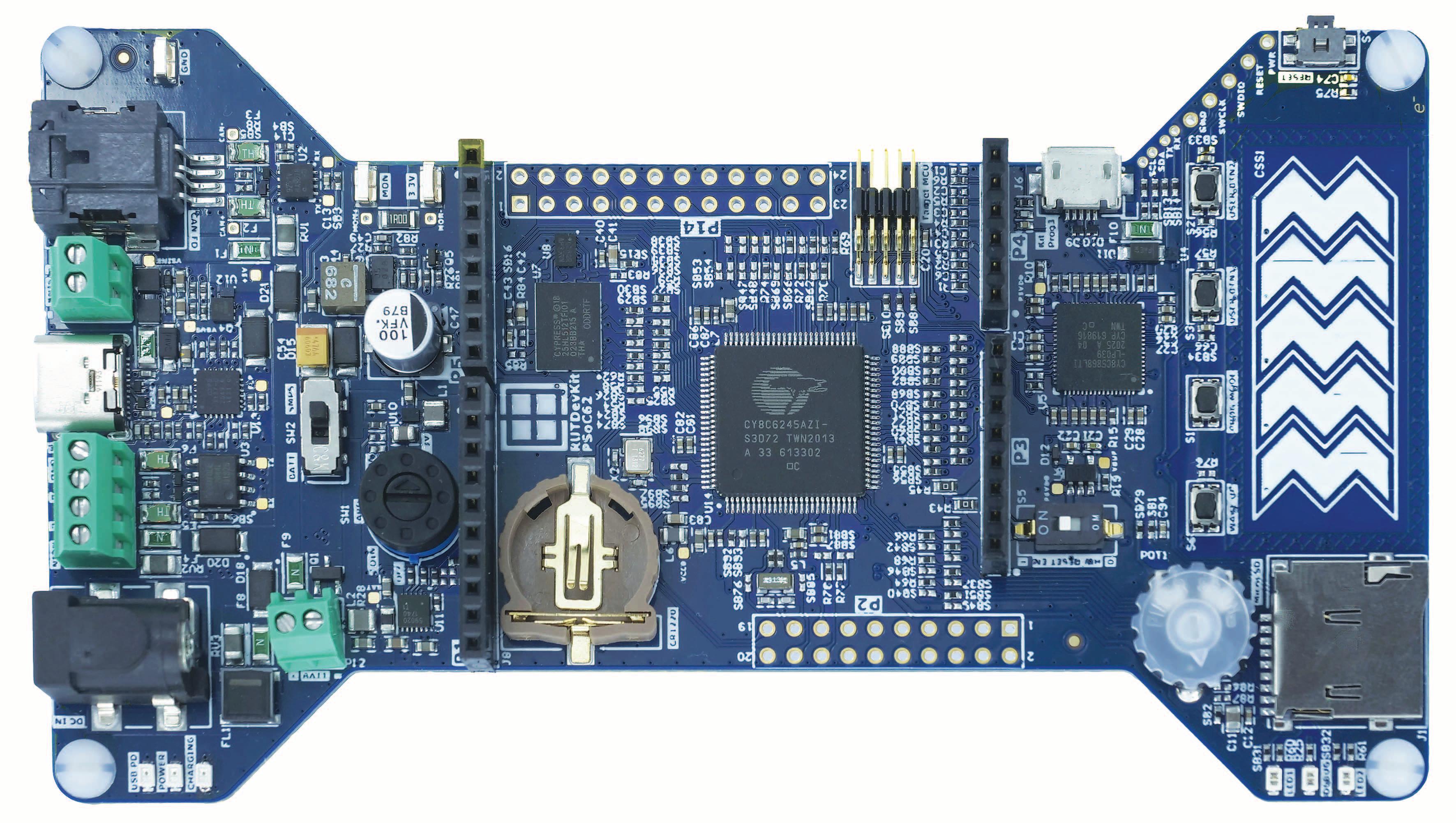
The basis for the RDK2 is the PSoC62 (Programmable System on Chip) from Infineon. The ultralow-power microcontroller is based on 40 nm manufacturing technology and combines a dual-core Arm Cortex-M4 and Cortex-M0.
Due to the integrated rotary switch for selecting the switched-mode power supply (SMPS), the RDK2 offers many different operating options: It can be operated with a standard power supply, alternatively via USB Type-C or even with a coin-operated battery.
The BD83070GWL buck-boost converter can supply the Arduino Shields with 3.3V and 2A at the output from a single-cell Liion battery or any other voltage source between 2.0V and 5.5V.
The AP63357DV-7 buck converter can supply the Arduino Shields with 5V and 3A at the output from any external voltage source between 5V and 20V.
In addition to the USB interface, the RDK2 has an integrated CAN-FD and RS 485 interface for communication between various devices or components, such as sen-
sors or actuators. In combination with external PSRAM (64 Mbit QSPI) or NOR
Flash memory (512 Mbit Semper NOR
Flash with features for functional safety according to IEC 61508, e.g. Safe Boot or ECC), the development kit is particularly suitable for the development of wearables and sensors. Thanks to the microSD card slot, data can also be stored externally. For even greater flexibility when using the controller, all general-purpose inputs/outputs (GPIO) can be addressed via external pin connectors that can be soldered onto the kit.
44 Electronica Azi International | 3/2022 DEVELOPMENT BOARDS
© Rutronik
Authors: David Werthwein, Product Manager Digital Gintaras Drukteinis, Technical Support Engineer Rutronik
An integrated potentiometer helps with the first ADC adjustment and can also be used for subsequent applications. The integrated power management IC (PMIC) is powered by the emergency power supply, i.e. a battery or supercapacitor. It controls the power supply for the controller and for the rest of the system (sensors and actuators or Arduino shields). Activation is via push button or the real-time clock (RTC) alarm. This enables the implementation of energy-saving solutions for applications in the industrial and automotive sectors.
The USB-C plug combined with USB power delivery capability enables more power to be transferred in the same period as its USB-A and USB-B predecessors. Charging times can thus be reduced significantly. As such, the RDK2 also ensures conformity with the USB-PD specification.
For elegant and reliable touch applications
The CapSense technology of the PSoC62 provides high sensitivity for accurate touch response, even in noisy environments, and fast sensing times for elegant, reliable, and easy-to-use capacitive touch-sensing applications. To do so, it utilizes a patented Capacitive Sigma Delta (CSD) sensing algorithm, which provides capacitive sensing through a switched capacitor technique with a delta-sigma modulator.
With the KitProg3 from Infineon, debugging is possible directly via the board without an external debugger. KitProg is a lowlevel communication firmware for programming and debugging PSoC microcontrollers. KitProg3 uses the industry standard CMSIS-DAP as the transport mechanism, while USB bulk endpoints provide fast communication.
Infineon provides the IDE “ModusToolbox” free of charge for programming. It includes a collection of easy-to-use software and powerful stand-alone tools, e.g. configurators. They can be combined flexibly with any compilers, editors, debuggers, and revision control systems.
Easy to extend with adapter boards from Arduino
The RDK2 is designed in the shape of a butterfly. Arduino stackable headers are located in the middle, where users can plug in any Arduino shields.
For this purpose, Rutronik has developed software for loading the created text files from the PC to the RDK2 via an operable graphical user interface (GUI). An audio amplifier and a 3.5 mm jack socket can then be used to control the sentences from the kit and output them via the speaker.
• The RutAdaptBoard-HMS is based on the Anybus NP40 network processor from HMS. It can be controlled serially and output various Industrial Ethernet and fieldbus protocols. It enables the integration of optimized infrastructure components, such as switches for high-performance Ethernet. Additional ASICs and FPGAs are not necessary for communication. EtherCAT applications can be implemented with the TwinCAT PC software from Beckhoff. Add-ons to other protocols are currently under development.
Needless to say, other Arduino shields can also be combined with the RDK2. However, users are expected to carry out the necessary software adjustments themselves.
Further, Rutronik provides firmware and demo applications free of charge. All the components needed for custom designs are available directly from Rutronik.
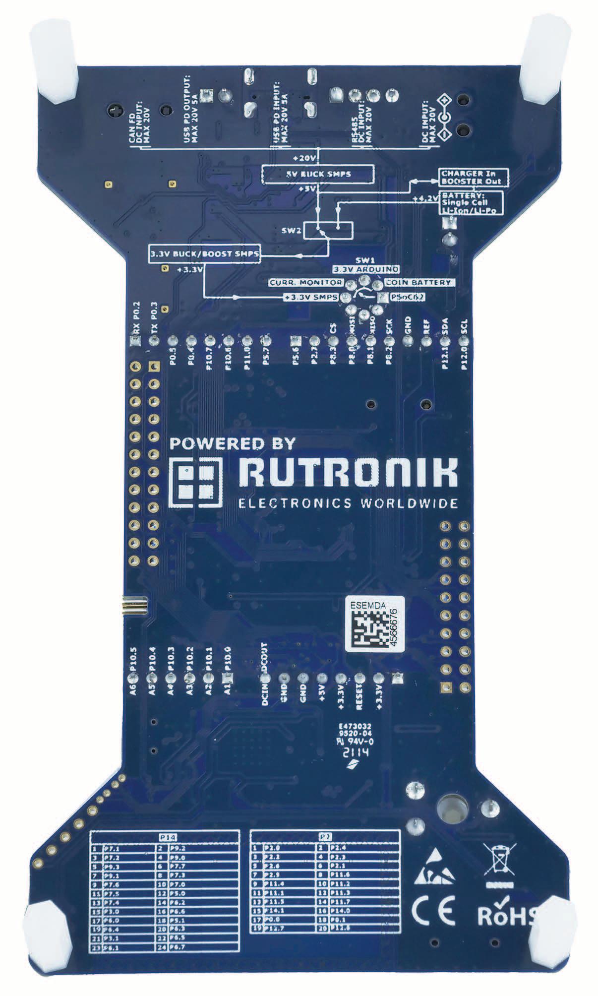

Further information on the RDK2 can be found at https://www.rutronik.com/developmentstories/rutronik-development-kit-rdk2/.
This unique design not only ensures a recognition factor but also high electromagnetic compatibility (EMC). Since the Arduino shields are suspended in the air, the flow of current is not disturbed at high frequencies, e.g. by copper on the board. Rutronik has already developed two such adapter boards and additionally provides the corresponding software stacks:
• The RutAdaptBoard-TextToSpeech shortens the development time for high-quality speech output. It comes with an integrated speech IC from Epson, which can output freely definable sentences in 12 languages with the help of corresponding PC software from the supplier.
The RDK2 offers many features to reduce development time for countless applications significantly. Under Rutronik System Solutions developed boards, like the RAB1 - Sensorfusion Board, the Adapter Board - Text To Speech, the RAB2 - CO2 or the HMS Anybus, can be stacked on the RDK2. In addition, all boards can be combined with each other, which provides even more possibilities for development. All components used for the boards are also available in Rutronik's portfolio.
■ Rutronik www.rutronik.com
https://international.electronica-azi.ro 45 DESIGN SOLUTIONS » The RDK2 based on the PSoC62 from Infineon
Encompassing Variety: Automation & Control at Digi-Key
By Eric Wendt Director of automation Digi-Key Electronics

So, while lead times for automation products have been extended a bit, and it may be more difficult for engineers to get the volume they have previously received, it’s not at the point where they’re on allocation, like some other commodities and raw materials.
As a distributor, Digi-Key is fortunate to be able to offer many different brands and products – some that complement each other, others that may compete – in order for the end customer to find exactly what they want for their project or production line. Some customers may design automation
products all on a specific brand platform, while others may use many different brands for different things. Then there are the ancillary, but necessary, products like wire, wire duct, interconnect and more. Purchasing from a distributor gives you the ability to order everything in the same cart.
We work closely with our supplier partners to give them as much visibility as possible into the products that are in highest demand, and in some cases, we’re already placing orders as far out as late 2023 to ensure that our inventory is pipelined accordingly.
Demand is high across all industries and verticals, including automation and control, so lead times are stretched in all product categories. While keeping inventory in stock is still a challenge, our inventory levels are growing month-overmonth. Over the past two quarters, we have received the most product per quarter that we have ever received in the history of the company.
Advice for Engineers
We encourage engineers to create designs with components that can be sourced from multiple suppliers.

Electronica Azi International | 3/2022 46
Current supply chain issues are affecting everyone around the world, and while automation products are certainly not immune to those challenges, they don’t have quite as many components in them as some of the consumer products.
© Digi-Key Electronics
▶
Digi-Key Electronics cut the ribbon on its new 204,400-square-meter Product Distribution Center expansion (PDCe) in Thief River Falls, Minn., in August 2022.
Of course, they can’t do that for every part, but there are often ways to reconfigure a design in a few ways using different part numbers. Having a bill of materials for parts with different manufacturers creates some insurance in the event that stock is not available. Our goal is to make it as easy as possible for customers to find alternative solutions that may fit their needs. When a customer tries to order a part number from our website and it is out of stock, Digi-Key automatically presents potential alternatives from our database of nearly 60 million part number cross-references. One of the many benefits of working with Digi-Key is that we have rich part associations on our website – meaning that if you’re searching for a specific sensor, for example, you can easily find the cable and bracket that go with it. We want to make it as easy as possible to get everything you need for a certain project. We are expanding our configuration and part selection tools to make the specification process even easier.
Our sales and technical support teams also handle many customer inquiries to help engineers find part cross references to replace out-of-stock components in their designs or to qualify multiple options in their designs.
In some cases, we are seeing engineers redesigning their end products to use parts that we have in stock; or starting the design by searching our website for instock product and designing their product around available inventory. Digi-Key is known for our wide breadth of product, with millions of products in stock and ready to ship immediately, resulting in no lead times for in-stock products. We also have a marketplace that allows suppliers with specialty products to sell online through our site. Having such a wide variety of products in stock allows us to ship nearly 99% of all orders the same day they are placed.
98% of all picks originate from our KNAPP OSR system to minimize errors and vastly improve efficiency and order volumes from our Thief River Falls facility so that our customers can be assured they will get the right parts every time. This high level of automation improves efficiency by up to 35% for picking and provides a great improvement in packaging quality and efficiency. The PDCe also features two primary sorting systems to provide redundancy in the case of a breakdown and provide opportunities for future growth. Creating a team-friendly work environment while also planning for scalability and growth were top of mind in the plans and design
Automation at Digi-Key
Digi-Key is unique in our service to customers with our automated systems designed to ensure customer’s orders ship the same day. Digi-Key has developed many proprietary systems to aid in ensuring our customers get the right part in the right quantity every time.

In August, Digi-Key opened the doors to our brand-new, 204,400 square meter Product Distribution Center expansion (PDCe). This expansion dramatically increases the amount of space available for storing existing and new products. In addition, expanded automation within the PDCe will decrease turnaround time and boost same-day order fulfilment to customers. The largest part of our newly automated system is the KNAPP OSR (order storage and retrieval) which provides the right parts to the picker every time, eliminating walk time and providing an ergonomically appropriate environment for the person doing the picking.

of the new building. There are areas of the facility currently left open with plans for future expansion.
There are over 43 kilometers of automated conveyor belt in the new facility, and an average order will travel more than 975 meters inside the building.
Looking Ahead
The automation and control market is booming and will continue to grow and move in very exciting directions. Digi-Key is ready to help drive technology innovation into 2023 and beyond with detailed technical resources and robust search functionality to help customers find the exact products they need to take their designs to the next level.
■ Digi-Key Electronics www.digikey.com

https://international.electronica-azi.ro 47 DESIGN SOLUTIONS » The Distribution Market Challenges
There are over 43 kilometers of automated conveyor belt in Digi-Key’s new PDCe, and an average order will travel more than 975 meters inside the building.

NXP Introduces High-Performance S32K39 Series MCUs for Modern Electrification Applications
NXP Semiconductors announced a new S32K39 series of automotive microcontrollers (MCUs) optimized for electric vehicle (EV) control applications. The modern S32K39 MCUs take electrification into the future with highspeed and high-resolution control for increased power efficiency to extend driving range and provide a smoother EV driving experience. The S32K39 MCUs include networking, security and functional safety capabilities beyond traditional automotive MCUs to address the needs of zonal vehicle E/E architectures and software-defined vehicles. The new MCUs enable NXP’s battery management system (BMS) and EV power inverters to provide end-to-end solutions for next-generation EVs.

The high-performance S32K39 MCUs are optimized for the intelligent and high-precision control of traction inverters that convert the EV battery’s DC power into alternating current to drive modern traction motors. The MCUs support traditional insulated-gate bipolar transistors (IGBT), as well as newer silicon carbide (SiC) and gallium nitride (GaN) technologies. With dual 200 kHz control loops to improve power efficiency, these can enable smaller, lighter, more efficient inverters, allowing motors to deliver a longer driving range. They can also control six-phase motors with increased power density and fault tolerance for improved long-term reliability. A safe ASIL D software resolver,
along with integrated sine wave generation and sigma delta converters, eliminate external components for reduced overall system cost. The S32K39 also provides flexibility to control up to quad traction inverters when coupled with the NXP S32E real-time processor and can implement advanced traction capabilities for 4wheel drive EVs in this configuration. Because of its versatile architecture, the S32K39 series is well-suited to address a wide range of EV applications beyond traction inverter control, including battery management (BMS), on-board charging (OBC) and DC/DC conversion. With support for hardware isolation, time-sensitive networking and advanced cryptography, it is well-positioned to support softwaredefined vehicles and zonal architectures.
About the S32K39
• Highest performance member of the S32K family with four Arm® Cortex®-M7 cores at 320 MHz configured as a lockstep pair and two split-lock cores
• Up to 6 MB of flash memory and 800 KB of SRAM
• Two motor control coprocessors and NanoEdge™ high-resolution pulse-width modulation (PWM) for higher performance and precision control
• Safe ASIL D software resolver eliminates external components and reduces cost
• Integrated DSP for flexible digital filtering and machine learning (ML) algorithms
• Multi-channel analog support with SAR and sigma-delta A/D converters, comparators and sine wave generators for resolver excitation
• Six CAN FD interfaces, TSN Ethernet and many advanced programmable I/Os
• Hardware security engine (HSE) for trusted boot, security services, secure overtheair (OTA) updates using Public Key Infrastructure (PKI) and key management
• S32K37 versions (without the two motor control processors) are also available
• Developed with certified ISO/SAE 21434 cybersecurity and ISO 26262 functional safety processes
• Available in two packages: 176LPQFP-EP and 289MAPBGA
System Solution Availability
Engineering samples, evaluation boards, and a comprehensive set of software support and tools are now available for lead customers. The S32K39 MCUs can be combined with the NXP FS26 safety system basis chip (SBC) and the advanced high voltage isolated gate driver GD3162 with adjustable dynamic gate strength control for a safe inverter control system. Both support the highest level of functional safety (ASIL D) for traction inverter development. Production release is planned for Q4 2023.
https://international.electronica-azi.ro 49
NXP Semiconductors https://www.nxp.com
COMPANIES
Get Smart about using Conductive Elastomers

For Electrical Bonding in Mil -Aero Connectors
Electrically conductive gaskets improve the EMI shielding of metal and metallised enclosures, while also enhancing electrical bonding and, in some cases, structural grounding.
Author: Gerard Young, Applications Engineer
These connections are primarily RF bonds and not electrical safety connections designed to carry high currents in the case of a short or malfunction. They may also provide part of the lighting strike (LS/EMP) protection of an aircraft, although this is very much a minor secondary function as other structures will carry most of the current. This resistance can be as low as 2.5mΩ and is not difficult to achieve if you have metal bonding straps linking the two parts of the structure. In some instances, however, such as a typical Mil-C-38999 connector, straps are not possible or convenient. Instead, the screws alongside a conductive flat or O-ring gasket facilitate the bonding of the connector to the housing.
Unfortunately, a, phenomenon sometimes occurs with connections of this type: electrical resistance will typically start at a value of R mΩ, before gradually increasing over a period of days or weeks to three or four times the initial value for no apparent reason, while sitting in a totally benign environment.
Many often consider the cause of this issue to be gasket instability, and in the case of flat gaskets this can sometimes be true due to over-compression. Conductive flat gaskets generally have a maximum deflection of around 15% of their initial thickness. The avoidance of damage by overzealous tightening of the fasteners is notoriously difficult due to thickness variations of typically ±10% to ±20%. This phenomenon is also apparent when using jam-nut or O-ring seals; even though there is metal-to-metal contact, resistance still increases over time.
The mechanisms
In order to understand this phenomenon we need to look at the physical and electrical model of the joint, identify the conduction paths and quantify their contribution to overall joint resistance. We also need to identify mechanisms that are likely to result in increased resistance. Figure 1 shows an example of a connector test fixture with the gasket in blue and the top and bottom plates representing the connector cover and housing respectively, held together with four M3 fasteners. In the adjacent electrical schematic:
Electronica Azi International | 3/2022 50
Parker Hannifin Chomerics Division Europe
Figure 1: Connector test fixture and resistance model.
• Rb represents the bolt resistance
• Rc is the connector coating resistance
• Rg signifies the gasket resistance

• Rh denotes the housing coating resistance
We can ignore the resistance of the actual metal in the housing and connectors as it is orders of magnitude smaller that these other resistances. In this scenario there are two possible conduction paths:
• Through the gasket
• Through the contact between the screw head and connector cover, and onwards through the fastener body and housing threads
Avoid over-compression
The important fact to note here is that if a flat conductive EMI gasket remains undamaged, its overall contribution to joint resistance is very small, with the majority coming from the ‘conductive’ chromate coating. Now, as mentioned earlier, some assemblies do actually manage to achieve <10mΩ contact resistances (though very small connectors), which gradually increase with time. With flat gaskets, this is normally a result of electrical connection through the bolts, which scrape off any chromate plating on the threads to provide a small area of intimate metal contact upon tightening.
An area of this size is easily achievably when tightening the screws on the connector if the screws are conductively finished and the action scrapes off the chromate coating. A couple of threads on one screw with that area of contact will give a resistance of 2.15mΩ in parallel with the 7.49mΩ of the gasket (436mm²).
Since this resistance is in parallel with the resistances of Table 2, using the formula for resistances in parallel gives a result of 1.67mΩ.
A key point here is that these fastener contacts are not stable, especially if any over-compression is evident.
Rb is in parallel with the other resistances and, if there is metal-to-metal contact via the threads, this can initially result in low contact resistance. However, as the contact oxidises or the pressure on the threads reduces due to the gasket gradually acquiring some compression set, this path may disappear entirely or exhibit a significant resistance increase.
Now, let’s assume the following:
• The housing and connector are made from aluminium alloy
• Both are treated with a MIL-DTL-5541, Type II, Class 3 conversion coating
• A specific resistance of no more than 2.5mΩ/in² is evident on each surface; a total of 5mΩ/in² through the specimen as per the specification
The table summarises the gasket and surface properties, and the contribution each gives to the resistance of the joint (ignoring any contribution from the fasteners). The area of the gasket is that of a Mil-C38999 connector gasket shell size 19 (around 4.8cm² or 0.75in²). It is possible to calculate the through-resistance of this gasket using the formula R=ρL/A, where:
• ρ is the volume resistivity in Ω cm
• L is the thickness in cm
• A is the area in cm²
The volume resistivity of clean aluminium is around 2,65*10-6ohm cm, or just over 3000 times less than a gasket at 0.008mΩ cm. As a result, achieving the same 10mΩ through-resistance with just metal contact via a 0.81mm thick contact thickness requires an area of 0.01mm².
In this case, the gasket will move slowly with time, typically at the corners, reducing the loads on the bolts.
The result is loss of contact on the threads, loss of pressure on the gasket and, subsequently, an increase in resistance.
DESIGN SOLUTIONS » Moulded gaskets for aerospace connector applications https://international.electronica-azi.ro 51
©
CHO-SEAL® 1285 volume resistivity 0,008 ohm cm Gasket thickness 0,081 cm Gasket area 4,36 cm² Unit resistance surface 1 0,016 ohm/cm² Unit resistance surface 2 0,016 ohm/cm² Table 1: Joint properties Gasket resistance Rg 0,00015 ohm Resistance of surface 1 Rc 0,00367 ohm Resistance of surface 2 Rh 0,00367 ohm Total resistance 0,00749 ohm % Age of total resistance due to Gasket 1.98% Table
Al volume resistivity 2,65*10-6 Ω cm Al thickness 0,081 cm Thread contact area 0,0001 cm² Table 3: Thread contact properties Al/screw resistance Rb 0,00215 Ω Gasket/surface resistance R 0,00749 Ω Total resistance Parallel resistance 0,001668 Ω Table
Figure 2: Gasket dimensions.
CODICO
2:
Joint resistances
4: Thread contact in conjunction with gasket
Even if the gasket remains undamaged by over-tightening the screws, it is still likely to exhibit some compression set, delivering a smaller compressive load on the gasket and a resultant increase in through-resistance.
Gasket selection
The shortcomings of a flat conductive EMI gasket die-cut from sheet material can be overcome in two ways:
• Use an O-ring or D-ring in a groove
• Use a moulded ‘flat’ gasket with features in conjunction with compression stops, either on the housing or connector, or within the gasket itself
With this thought in mind, the joint either needs bare metal-to-metal contact, accepting that it’s necessary to damage the chromate surface, or use something like a bonding strap that you fasten tightly against the bare metal surface. The second option, where we effectively replace a flat gasket with a moulded one (possibly with compression stops), offers a more useable and reliable option but it will be more expensive.
Size and customisation
In summary, electrically conductive flat gaskets for electrical bonding in militaryspecification aerospace connectors work

Coating Resistance
A MIL-DTL-5541 Type II Class 3 coating will always be a major part of the resistance of any conductive joint, because the conversion coating has a volume resistivity of around 45Ωcm and is between 0.25 and 0.5 μm thick (10-20 micro-inch). In comparison, a gasket has a volume resistivity of between a few milliohm cm to a few ohm cm.
In the event you do manage to achieve low milliohm resistances on very small connector gaskets, it’s likely that you have damaged the chromate conversion coating on either the housing or connector surface or in the bolt threads, and this low bonding resistance is unlikely to be stable. On the other hand, if your connector is large enough, or you have, for example, four connectors with gasket areas of around 3.2cm² (0.5in²) or more, you should be able to achieve a low milliohm bonding requirement. If you do not have enough area, then you may need to consider something like a plated finish rather than a conversion coating.
Regarding O-rings, there are two factors to consider (as with flat gaskets):
• The area of contact provided by the O-ring
• The area of metal-to-metal surface contact (not including the screw threads)
If we again consider a connector of the shell size 19, a suitable O-ring may have an inside diameter of around 40mm and a cross section of 1.78mm. If designed correctly, we can estimate the contact area will be the full width of the groove. This gives a contact area for the gasket of around 257mm² and a thickness of around 1.45mm, so the resistance of the gasket in conjunction with the chromated surfaces will be 17mΩ. As a result, we must calculate a parallel metal-to-metal contact area to achieve resistance below 10mΩ. Using the formula for resistances in parallel, we find that the metal-tometal contact resistance needs to be around 20mΩ. If this is through perfect contact with the chromated surface at 5mΩ/in², we’ll need 0.25in² (1.6cm²) of contact, which is possible but unlikely.
so long as they are large enough and remain undamaged by the load applied by the screws. O-ring gaskets also work and offer protection from over compression, but have a reduced area of contact compared with a flat gasket. With its customisation potential, a moulded gasket offers the optimal solution for aerospace connector applications. Although it will cost slightly more than either a flat gasket or O-ring in terms of its purchase price, a moulded gasket delivers numerous design and cost of ownership advantages. For instance, you’ll typically need less seal material in comparison with die-cut gaskets, thereby reducing costs in
many applications, while it is also possible to meet compression/deflection requirements with fewer fasteners, resulting in better maintainability. Furthermore, design engineers can place fasteners inboard or outboard of the gasket more easily, reducing both EMI and moisture leakage into the enclosure through fastener holes.
Production savings are also available as the gasket, cover and compression stops become a single part, reducing the number of purchased items, inventory and documentation. As a final point, by using moulded gaskets you can eliminate inconsistent and expensive bonding operations.
■ Chomerics | www.parker.com/chomerics
Electronica Azi International | 2/2022 CONNECTORS
52
Newest u-blox automotive multi-band GNSS module enables ADAS applications up to 105°C
The ZED-F9K-01A high-precision AEC-Q104 GNSS module offers a fully integrated and reliable lane identification solution.
u-blox has announced the u-blox ZED-F9K-01A, a high-precision GNSS module with embedded advanced hardware, software, and latest generation IMU (Inertial Measurement Unit) to provide an advanced, self-contained positioning solution. The module supports both L1/L2/E5B and L1/L5 bands for maximum flexibility, satellite availability, and security. It combines multi-band and multi-constellation global navigation satellite system (GNSS) technology with dead reckoning high-precision RTK (real-time kinematic), which enables decimeter-level accuracy.
The u-blox ZED-F9K-01A natively supports the u-box PointPerfect GNSS augmentation service. It delivers multiple GNSS and IMU outputs in parallel to support all possible architectures, including a 50 Hz sensor-fused solution with very low latency. It enables advanced real-time applications, while the optimized multi-band and multi-constellation capability maximizes the number of visible satellites even in urban conditions.
ZED-F9K-01A includes a dependable protection level output and advanced security features including anti-spoofing and anti-jamming. Operation up to 105 ºC makes it possible to integrate the product anywhere in the car without design constraints.
“The u-blox ZED-F9K-01A primarily targets ADAS applications, paving the way to full car autonomy. Being a fully integrated solution that includes the latest u-blox R&D technology for automotive, it helps OEMs greatly reduce their development efforts and time to market,” says Martin Wallebohr, Senior Product Manager Automotive GNSS, at u-blox
ZED-F9K-01A will be on display at the upcoming CES 2023 tech event in Las Vegas, US at booth #10923. Samples of ZED-F9K01A are already available for evaluation.
■ u blox | https://www.u-blox.com/en
Renesas Unveils First Family of Automotive Radar Transceivers with Industry’s Highest Accuracy and Lowest Power Consumption

RAA270205
4x4-channel, 76-81GHz Radar Transceiver Incorporates Technology Through Recent Acquisition of Steradian to Build Out Renesas’ ADAS Sensor Fusion Portfolio
Renesas Electronics Corporation is entering the automotive radar market with the introduction of a 4×4-channel, 7681GHz transceiver designed to meet the demanding requirements of ADAS (advanced driver assistance systems) and Level 3 and higher autonomous driving applications. Leveraging automotive expertise accumulated through years of global customer engagements, Renesas will incorporate the new RAA270205 high-definition radar transceiver into its growing sensor fusion portfolio, which combines radar, vision systems, and other sensing modalities. Designed in cooperation with Steradian Semiconductors Private Limited, which Renesas acquired earlier this year, the RAA270205 was featured in a Renesas product showcase at electronica, Munich, Germany, November 15-18, 2022. The new transceiver MMIC (monolithic microwave integrated circuit) is especially suited for imaging radar, long-range forward-looking radar and 4D radar, but can also be used for corner and central-processing radar architectures, the socalled “satellite” automotive radar systems.
Electronica Azi International | 3/2022 54
PRODUCT NEWS
Equipped with 4Tx and 4Rx channels, the RAA270205 supports up to 16 MIMO (multiple-input and multiple-output) channels. It can be cascaded to enable higher channel count and better radar resolution.
The RAA270205 features best-in-class accuracy with up to 5GHz of bandwidth, and a 112.5MSPS ADC (analog-to-digital converter) sampling rate that is nearly three times faster than competing devices. Power consumption of 1.2W is 50 percent lower than comparable transceivers and it delivers a noise figure of 9dB, which is 3dB less than other radar transceivers. Its superior chirp rate of up to 300MHz/μs improves radar resolution and object detection.
“Today’s radar transceiver MMICs must achieve higher definition to support the high-accuracy requirements of ADAS and autonomous driving safety platforms,” said Vivek Bhan, Senior Vice President and Deputy General Manager of Renesas’ Automotive Solution Business Unit. “Working in close collaboration with Steradian, which brings deep radar design expertise, we are expanding our sensor fusion offerings with a focus on functional safety and low power consumption to help our customers lower their development costs and improve time to market.”
RAA270205 Winning Combinations
Renesas has plans to combine the RAA270205 transceiver with other compatible devices from its portfolio to support automotive radar systems. These Winning Combinations will include the “Satellite Radar System for AD/ADAS”, which will be available in Q2/2023. Renesas Winning Combinations are technically vetted system architectures from mutually compatible devices that work together seamlessly to bring an optimized, low-risk design for faster time to market. Renesas offers more than 300 Winning Combinations with a wide range of products from the Renesas portfolio to enable customers to speed up the design process and bring their products to market more quickly. They can be found at renesas.com/win.
■ Renesas Electronics Corporation
https://www.renesas.com
u-blox and GMV partner to develop market ready end-
safe positioning solutions for ADAS
u-blox (SIX:UBXN), a global provider of leading positioning and wireless communication technology and services, and GMV, a leader in safe positioning systems, have partnered to provide ready-to-use functional safe positioning solutions.
Functional safety is becoming increasingly indispensable for automated or autonomous driving vehicles within the automotive and industrial sectors.

Currently, customers must spend significant effort to develop and integrate hardware and software from several vendors for a functional safe positioning solution. GMV’s leading safety algorithms and augmentation service combined with u-blox leading positioning hardware and software will be integrated in a ready-to-use solution. The offering is designed to save efforts and accelerate time-to-market while enjoying the advantage of a cost-effective, proven functional safe positioning solution.
The unique, ready-to-use functional safe positioning solution will be marketed by u-blox complementing its existing GNSS receiver portfolio and advanced GNSS augmentation service PointPerfect.
Further details will be announced in early 2023.
■ u blox | https://www.u-blox.com/en
https://international.electronica-azi.ro 55
to-end
COMPANIES
onsemi’s New Approach to Inductive Position
Sensing Speeds Up Time-to-Market
onsemi introduced an innovative dual-inductive rotary position sensor, which convinces with its speed and accuracy. The NCS32100 uses a newly patented approach to inductive position sensing, making it an ideal choice for industrial and robotic applications, where fast-moving robotics and machinery are deployed. While the features of inductive encoders make them very appealing for industrial applications, they have historically been limited to use cases that do not require a high degree of accuracy and operate with low rotational speed. With the NCS32100, onsemi leveraged its 20+ years of expertise designing inductive sensors to combine the reliable benefits of inductive encoders with the accuracy and speed generally associated with mid- to high-end optical encoders. Using a 38mm sensor, the device delivers +/-50 arcsec accuracy at 6,000 RPM. The NCS32100 can support speeds up to 100,000 RPM with reduced accuracy.
Inductive sensors have several key features that make them desirable for industrial applications including low sensitivity to almost all forms of contamination or interference, robustness against mechanical vibration, and no first-order temperature dependence. The NCS32100 device also features an integrated calibration routine to account for mechanical misalignment in the sensor. High levels of configurability enable use with a wide range of printed circuit board (PCB) sensor designs, giving OEMs the ability to configure and differentiate their solutions. The integrated MCU includes non-volatile flash memory (NVM) and a configurable interface for communication with the host processor.
Reference designs and evaluation boards are available to further accelerate the design process for industrial applications. The NCS32100 is available now through onsemi sales support and authorized distributors.
■ onsemi | https://www.onsemi.com
Renesas Lays Out WiFi Roadmap Based on Technology from Celeno Acquisition
Renesas Electronics Corporation unveiled plans to deliver a comprehensive set of advanced Wi-Fi offerings to complement its broad portfolio of Industrial and IoT products. Renesas completed its acquisition of Celeno last year and is leveraging that technology to address a wide range of Wi-Fi client and access point applications for Wi-Fi 6/6E and Wi-Fi 7. Today, Renesas is delivering production volumes of high-performance Wi-Fi 6E access point solutions with its CL8000 family.
Renesas is also sampling a powerful, highly integrated, 2×2 Wi-Fi/BLE combo chip supporting Wi-Fi 6E tri-band switchable radio (6GHz, 5GHz & 2.4GHz), 160MHz channel bandwidth and up to 2.4Gbps Data Link Speed. The new low-latency, highly secure chipset includes Bluetooth and BLE 5.2 support, and addresses multimedia streaming applications, IoT gateways and cloud connected devices. Renesas is also developing a Wi-Fi 6E chipset with unique, patented Wi-Fi Doppler Imaging technology. This Wi-Fi Radar technology depicts the range and doppler signature of people and objects using standard Wi-Fi signals. It eliminates the need for multiple cameras or sensors in home environments and commercial buildings. For example, it can be used to detect the presence and location of people in a room to redirect and optimize airconditioning flows, saving on energy costs.
56
Electronica Azi International | 2/2022
Another example could be intrusion detection to secured facilities or connected cameras with motion sensing to activate the camera. The combined connectivity and sensing chip is currently scheduled for production in the next 18 months. Wi-Fi 7, also known as Extremely High Throughput (EHT), will deliver significantly faster throughput by employing faster modulations and double the bandwidth. In the 6GHz band, WiFi 7 would more than the double the maximum speed and will increase speeds in the 2.4GHz and 5GHz band by as much as 30 percent. More importantly, some prominent features of Wi-Fi 7 will improve network reliability, latency and user experience. For example, by delivering Multi Link Operation, devices would monitor multiple links across different bands and provide consolidated operation to optimize interference and retransmission avoidance. Users will benefit from more reliable networks and from lower and more predictable latency. Wi-Fi 7 is expected to launch in 2024 with early adoption in mobile phones, computers and networking devices. Broader adoption in IoT, industrial and consumer multimedia applications will follow. Renesas’ Wi-Fi 7 offerings will include solutions for home networking, IoT, industrial and consumer multimedia devices.
Winning Combinations
Renesas offers numerous Winning Combinations that combine Wi-Fi 6 and 6E chipsets integrated with a broad range of solutions from Renesas, including embedded processing, analog, power, timing and connectivity products. These engineering-vetted Winning Combinations will span applications from a High Throughput Wi-Fi 6 Router for home gateways to a Wireless IEEE 1588 Solution for 5G networks. More Winning Combos with Wi-Fi 6 are under development, including a Video IP Phone, Smart Home Security Terminal, and expansion of the Renesas Quick-Connect IoT Platform to include a Wi-Fi 6 USB stick for users to rapidly build prototypes.
■ Renesas Electronics Corporation


https://www.renesas.com
Nexperia launches new hotswap Application Specific MOSFETs (ASFETs) with double the improvement in SOA

Nexperia, the expert in essential semiconductors, today extends its ‘ASFETs for Hotswap and Soft Start’ portfolio with the introduction of 10 new 25 V and 30 V fully optimized devices, combining industry-leading enhanced safe operating area (SOA) performance with extremely low RDS(on), making them ideal for use in 12 V hotswap applications including data center servers and communications equipment.
For several years, Nexperia has been combining proven MOSFET expertise and broad application understanding to develop market-leading ASFETs, devices in which critical MOSFET performance characteristics are enhanced to meet the requirements of particular applications. Since the launch of ASFETs, success has been seen with products optimized for battery isolation, DC motor control, Power-overEthernet, automotive airbag applications and more.
In-rush currents can present a reliability challenge in hotswap applications. Nexperia, the original pioneer of enhanced SOA MOSFETs, has addressed this concern by designing a portfolio of ‘ASFETs for Hotswap and Soft Start with enhanced SOA’ that are fully optimized for such applications. The PSMNR67-30YLE ASFET delivers 2.2x stronger SOA (12 V @100 mS) than previous technologies while having an RDS(on) (max) as low as 0.7 mΩ. The Spirito effect (represented by the steeper downward slope found on SOA curves at higher voltages) has been eliminated, while exceptional performance is maintained across the full voltage and temperature range (compared to unoptimized devices).
Nexperia further supports designers by removing the need to thermally de-rate designs, by fully characterizing these new devices at 125 °C and providing hot SOA datasheet curves. With eight new devices (three 25 V and five 30 V) available in a choice of LFPAK56 & LFPAK56E packages with RDS(on) ranging from 0.7 mΩ to 2 mΩ, the majority of hotswap and soft start applications are addressed. Two additional 25 V products (which will have an even lower RDS(on) of 0.5 mΩ) are planned for release over the coming months.
For more information, please visit:
https://www.nexperia.com/products/mosfets/applicationspecific-mosfets/asfets-for-hotswap-and-soft-start/
■ Nexperia | https://www.nexperia.com

57
https://international.electronica-azi.ro PRODUCT NEWS
3.5” embedded board for IoT applications
With the WAFER-EHL ICP-Germany expands its portfolio in the area of embedded boards.
The WAFER-EHL is a 3.5″ mainboard which has a cooling shell. This allows a very simple installation of the board as well as an uncomplicated heat dissipation of the installed components, which is an advantage for machine builders or mechanical engineers. The WAFER-EHL 3.5″ embedded board is equipped with an Elkhart Lake Celeron® J6412 processor, which has four processor cores. The Elkhart Lake generation is designed for IoT edge devices and brings features in IoT, real-time performance and functional security, among others. In addition, performance has been increased by up to 1.7X in single-thread performance and up to 1.5X in multi-thread performance compared to the previous generation. Thanks to Intel® Gaussian & Neural Accelerator (GNA), audio-based neural networks can be executed at low power consumption, reducing CPU workload. The burst frequency of the Celeron® CPU is 2.60GHz. An 8GB DDR4 RAM module with 3200 MHz is permanently installed on the WAFER-EHL 3.5″ board as standard. For graphics output, the board is equipped with a display port with maximum resolution of 4096×2160 pixels and an HDMI port. An eDP, LVDS or VGA module can be added via the IEI IDPM 3040 slot. Particularly noteworthy is the PCIe x4 slot, which is a real special feature on the 3.5″ board and makes expansion with riser cards possible. As network ICs, two Intel i225V were used, which allow a speed of up to 2.5GbE each.
Specifications
• 3.5″ CPU board with heat spreader cooling concept
• Intel® 10nm Elkhart Lake Celeron® processor
• Max. 8GB DDR4 SO-DIMM memory
• Expandable through PCIe x4 slot
• Three independent displays: HDMI, Display Port and
Fanless embedded PC for 10th generation Intel
Core I processors
With the E410-13CMI embedded system, ICP Germany expands its portfolio with a low-cost and high-performance IPC variant. The E410-13CMI supports 10th generation Intel® CoreTM I3, I5, I7 and I9 desktop processors with up to 10 processor cores and 35 watts. Up to 64GB DDR4 SO-DIMM memory with a clock frequency of 2933MHz can be installed on the two DIMM sockets.
The Intel® HD graphics unit offers dual display support. The E410-13CMI offers an HDMI and a Displayport port for connecting monitors. For storage media, a mini PCIe mSATA and an M.2 2280 slot with SATA signal are available in addition to the 2.5″ SATA mounting frame. Furthermore, the E410-13CMI offers two network ports with Intel® i219-LM GbE and i210-AT GbE network IC. Furthermore, four USB 3.0, 8 GPIO, six USB2.0 ports as well as audio functionality.
For expansion, there is an M.2 2230 E-Key with USB and PEX1 and Intel® Integrated Connectivity I/O Interface (CNVi), an M.2 2242/2280 M-Key with SATA and a Mini-PCIe with USB2.0, SATA and PEX1 signal. The E410-13CMI can be operated fanless in a temperature range from -20°C to 50°C. On request, ICP Germany can deliver the E410-13CMI as a ready-to-use system with suitable industrial memory modules and solid state disks.
optional IDPM
• Dual 2.5G network interface
• USB 3.2, SATA, COM
• Extensions: M.2 slots
Applications
• IoT
• Automation manufacturer
• Display systems
• Ultra flat embedded systems
• Point of sale applications
■ ICP Deutschland GmbH | https://www.icp-deutschland.de
Specifications
• Fanless Embedded PC
• 10th generation Intel® CoreTM I processors (Comet Lake)
• Intel® H420E chipset
• Max. 64GB DDR4 SO-DIMM memory
• Dual Display Support
• M.2 and mini PCI Express full size expansion slots
• USB, HDMI, DP, GbE, RS-232/422/485
Applications
• Automation
• Industrial control
• Machine Vision
• Data logger
• Industrial PC
Electronica Azi International | 3/2022 58
ICP Deutschland GmbH | https://www.icp-deutschland.de
■
PRODUCT NEWS