4/2021 A PAN EUROPEAN MAGAZINE https://international.electronica-azi.ro INTERNATIONAL


The MXT1296M1T provides various communication options, ISO 26262 functional safety support and flexible RF emission control
As the automotive market continues to demand larger touchscreens with more flexibility in size and shape, Microchip Technology Inc. is announcing a new maXTouch® touchscreen controller, that allows automotive designers to satisfy various and unique aspect ratios for touch displays in cars. This new offering includes additional functional safety support requested by OEMs.
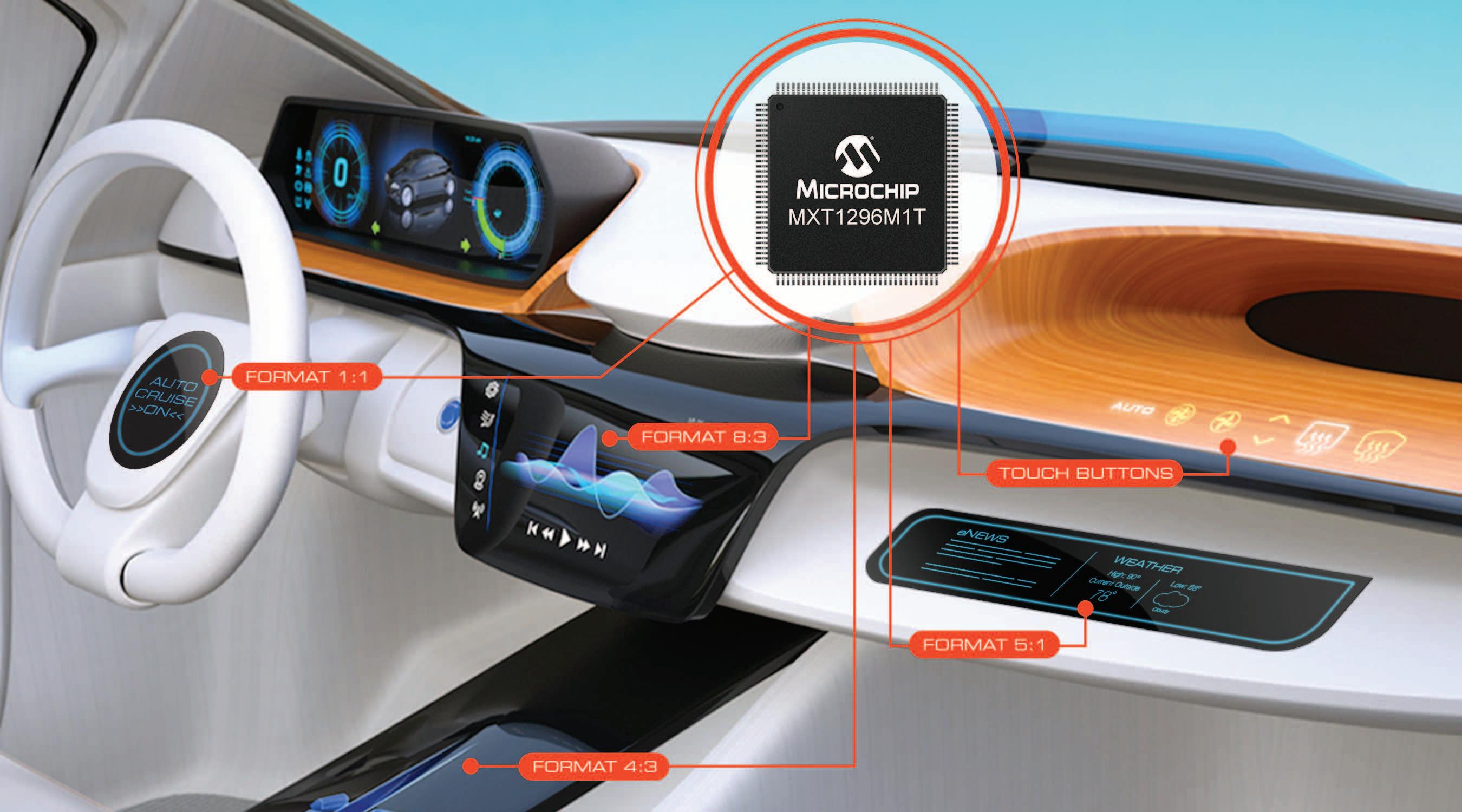
The MXT1296M1T can reconfigure its driving and receiving touch channels to match the exact screen format, from 1:1 to 5:1 aspect ratio, including the popular 8:3 automotive aspect ratio. This feature enables the customer to efficiently use the number of touch channels available, without the need to select a larger, more expensive touch controller. Furthermore, customers can save additional development and validation time and resources by reusing a common PCB design to support different touch sensor aspect ratios. The MXT1296M1T is an industry first to enable the sensor channel reconfiguration by parameters. These settings do not require firmware modification, leading to lower design risk and faster time to market.
“As touch displays have become more popular in automotive user interfaces, car manufacturers are using various display formats and shapes to accommodate their interior design and emphasize their brand identity,” said Clayton Pillion director of the human machine interface business unit at Microchip Technology . “As the number one automotive touchscreen controller supplier, we know that products with enhanced diagnostic features are a significant advantage to customers who are designing with unique features and increasing ISO 26262 functional safety requirements in-mind.”
Microchip’s new maXTouch touchscreen controller offers two communication interfaces operating simultaneously, which allow a bridgeless connection to the back channel of the LVDS video link for touch information and a connection to a local microcontroller (MCU). The bridgeless topology reduces touch latency to improve the user experience. It also guarantees full compatibility with the maXTouch software driver, available for all major automotive operating systems,
including Linux®, Android™ and QNX®. When connected to an appropriate local MCU, the second interface offers:
• A redundancy link to the head unit through a CAN bus or 10BASE-T1S automotive Ethernet link for increased functional safety at the system level
• Local access and control of the maXTouch touchscreen controller’s features such as a capacitive keys report, live touch sensor diagnostics and raw data for external and custom post-processing
• Over-the-air and secure firmware update capability using Microchip’s TrustAnchor100 companion chip
The MXT1296M1T embeds various functional safety features to constantly check the integrity of the touch controller operation, as well as that of the connected touch sensors. The Failure Modes Effects and Diagnostic Analysis (FMEDA) and functional safety manual, dramatically ease the customer experience to design, build and certify a system for Automotive Safety Integrity Level B (ASIL-B) applications to the ISO 26262 standard.
Microchip Technology


https://www.microchip.com


3 | Most Versatile maXTouch® Touchscreen Controller Ever Offers Extensive Screen Format Flexibility
6 | Renesas Launches Automotive Actuator and Sensor Control MCUs for Evolving Edge Applications in NextGeneration E/E Architecture

Applications Drives Multiple Configurations; Integrates Analog Power Components to Reduce BOM Cost & Board Space
40 | Digi-Key, Seeed Studio and Machinechat introduce industry’s first private LoRaWAN-in-a-Box Solutions
42 | Click: MIKROE adds high-performance signal generation for $109
43 | Round-the-clock accessibility
44 | Cost Effectively Meeting International Standards with Board Mounted AC/DC Power Supplies
47 | Verizon selects Infineon’s EZ-PD™ PAG1 AC-DC power solution for its 45 W USB-C fast wall charger
48 | Green Hydrogen - Myth or Reality?

52 | COSEL’s adds a 300W to its robust and reliable PJMA series of power supplies for demanding medical applications
7 | Microchip to Provide Silicon Carbide MOSFETs and Digital Gate Drivers for Mersen’s SiC Power Stack Reference Design


8 | Analog Devices’ People Counting Algorithm Ensures Efficient Space Utilization and Worker Safety
9 | Improved power density: alpitronic selects Infineon’s EasyPACK™ CoolSiC™ modules and EiceDRIVER™ X3 drivers for its 50 kW hypercharger
10 | How A2B Technology and Digital Microphones Enable Superior Performance in Emerging Automotive Applications
53 | Powerbox announces 700W power supply optimized for conduction cooling applications
54 | MicroSys puts Hailo AI performance on its SoM platforms with NXP S32G vehicle network processors
55 | SEGGER J-Link software now available for
18 | How rugged is rugged?
20 | The AI of Things
24 | Mouser Signs Global Distribution Agreement with Siretta to Deliver Leading-Edge IoT Mobile Broadband Technologies 26 | Trust platform provides security from concept to deployment
| Microchip Continues Expansion of Gallium Nitride (GaN) RF Power Portfolio
Implementation on MCUs
| Renesas Adds New Power Line Communication Modem IC Enabling High-Speed, Long Distance Communication, Expanding Practical PLC Applications

Rutronik Brings a Breath of Fresh Air

60 | Infineon and MCI supply sensors for air quality measurement to schools in Carinthia and Tyrol
62 | Sensor solutions for robot working areas
|
Pineapple 38 | Renesas Programmable Smart Gate Driver for BLDC Motor
Management
Managing Director - Ionela Ganea
Editorial Director - Gabriel Neagu

Accounting - Ioana Paraschiv
Advertisement - Irina Ganea
Web design - Eugen Vărzaru
Contributing editors
Cornel Pazara
PhD. Paul Svasta
PhD. Norocel Codreanu
PhD. Marian Blejan
PhD. Bogdan Grămescu
64 | Sensor solutions for pharmaceutical packaging
66 | Reliable object detection also with LED hall lighting
®
“Electronica Azi” is a registered trademark at OSIM - Romania, Registered position: 124259
ISSN: 1582-3490


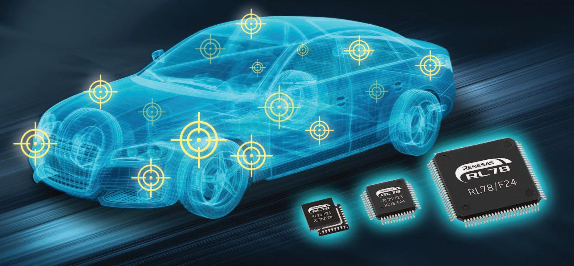
Renesas Electronics Corporation announced two new microcontrollers (MCUs) designed for automotive actuator and sensor control applications supporting edge evolution in next-generation electronic and electrical (E/E) architecture. With the new RL78/F24 and RL78/F23, Renesas expands its RL78 Family of lowpower 16-bit MCUs and strengthens its broader automotive portfolio, offering customers highly reliable, high-performance solutions for systems ranging from actuators to zone control.
With E/E architecture extending to include zone and domain control applications, control mechanisms are evolving to accommodate body control for automotive systems such as lights, windows, and mirrors; motor control for engine pumps and fans; and multiple sensor control. Moving forward, high-speed and secure connectivity with zone and domain controllers will be mission critical for edge electronic control units (ECUs). Renesas’ next-generation RL78/F24 and RL78/F23 MCUs address changing technology demands for actuator and sensor control with enhanced security, rich connectivity, and functional safety capabilities. The new devices support the CAN FD high-speed communication protocol (RL78/F24) and
EVITA-Light security and are optimized for systems targeting ASIL-B levels under the ISO 26262 functional safety standard.
“Advances in E/E architecture add stress to the already heavy development burden, and there is high demand among our customers to efficiently develop actuators,” said Naoki Yoshida, Vice President, Automotive Digital Products Marketing Division at Renesas. “Our new actuator and sensor control MCUs build on our highly popular RL78/F14 and RL78/F13 devices and enable developers to reuse most of their existing software assets, reducing costs while continuing to accelerate the advancement of E/E architecture.”
The future of automotive systems design lies in a vehicle-centralized, zone-oriented E/E architecture, and that shift is sparking higher demand for more advanced functionality and better performance in actuator controller applications. The new RL78/ F24 and RL78/F23 MCUs deliver up to approximately 70 percent faster operating frequencies than the previous generation, which can more than double the performance in brushless motor control (BLDC) applications. Renesas also enhanced the hardware accelerator and timer functions for motor control and added a 12-bit A/D
converter, offering customers the enhanced functionality and performance levels they demand.
Key Features of RL78/F24 & RL78/F23 MCUs
• 40 MHz operating frequency
• Supports several connectivity interfaces, including CAN FD (RL78/F24), LIN, SPI, & I2C
• EVITA-Light support security functionality (support for AES-128/192/256 encryption algorithms)
• Pin compatible with the RL78/F14 and RL78/F13 MCUs with the same power efficiency
• On-chip flash memory capacity of 128 KB or 256 KB
• Package lineup ranging from compact 5 × 5 mm 32-pin QFN to 100-pin QFP
• Support for high temperatures up to 150°C
• RL78/F24 Target Board and RL78/F24
12V Motor Control Evaluation System
Starter Kit soon to be released for RL78/F24 (under development)
Samples of the RL78/F24 and RL78/F23 MCUs will be available starting April 2022, and are scheduled to enter mass production in the second half of 2023.
Renesas Electronics Corporation
https://www.renesas.com
E-mobility and renewable energy systems require power management solutions that drive performance and cost efficiencies in addition to speeding up development time. To keep pace with these requirements, Microchip Technology Inc. announced the collaboration with Mersen on their 150 kilovolt-ampere (kVA) threephase silicon carbide Power Stack Reference Design. Mersen is a global provider of power management solutions for numerous industrial sectors including e-mobility and energy storage.
Mersen’s three-phase SiC Power Stack Reference Design provides system designers with a complete, compact, high-power silicon carbide solution without the need for individual device sourcing, testing and qualification. The Power Stack Reference Design includes Microchip’s silicon carbide power modules and digital gate drivers and Mersen’s bus bar, fuses, capacitors and thermal management, optimally designed together in a single high-performance stack reference design. With Microchip’s 1200V MSCSM120AM042CD3AG silicon carbide MOSFET and AgileSwitch® 2ASC12A1HP digital gate driver, the Power Stack Reference Design enables engineers to rapidly develop high voltage systems using kits predesigned for their applications – reducing time to market by up to six months.
“Microchip customers will benefit from our collaboration with Mersen to provide silicon carbide MOSFETs and digital gate driver solutions,” said Leon Gross, vice president of Microchip’s discrete product business unit. “When power inverter designers can source a proven solution, they can avoid sourcing individual parts and reduce risk through reliability – and that helps avoid downtime. Designers now have an all-in-one evaluation system.”
The Power Stack Reference Design provides 16 kilowatts per liter (kW/l) of power density and up to 130°C Tj, peak efficiency at 98%, with up to 20 kilohertz (kHz) switching frequency. Utilizing Microchip’s rugged silicon carbide MOSFETs and AgileSwitch family of configurable digital gate drivers, the reference design enables engineers to select from 700V and 1200V options in currents up to 750A. Microchip also provides a choice in module construction including baseplate material, Direct Bonding Copper (DBC) ceramic material and die attach method.
“We worked closely with Microchip on the design and development of this silicon carbide Power Stack Reference Design given the availability of highly robust silicon carbide MOSFETs and compatible digital gate drivers from a single source,” said Philippe Roussel, PhD, vice president, Global Strategic
Marketing Executive Expert at Mersen “Thus, we can demonstrate our ability to optimize any inverter topologies from our customers, relying on our line of highly reliable bus bars, capacitors, fuses and cooling systems. The versatile Microchip silicon carbide line-up also gives us the capacity to extend these primary specifications to higher voltage, current and switching frequency to meet every customer’s operating point needs.”
In addition to the products in Mersen’s Power Stack Reference Design, Microchip is a provider of other silicon carbide power solutions including families of MOSFETs and Schottky Barrier diodes from 650V to 1700V, available in bare die and a variety of discrete and multi-chip module packages.
Microchip unifies in-house silicon carbide die production with its low-inductance power packaging and digital gate drivers enabling designers to make efficient, compact and reliable end products. These devices pair well with a comprehensive portfolio of microcontrollers (MCUs), analog and MCU peripherals, plus communication, wireless and security technology, providing system designers across many applications with proven total system solutions.
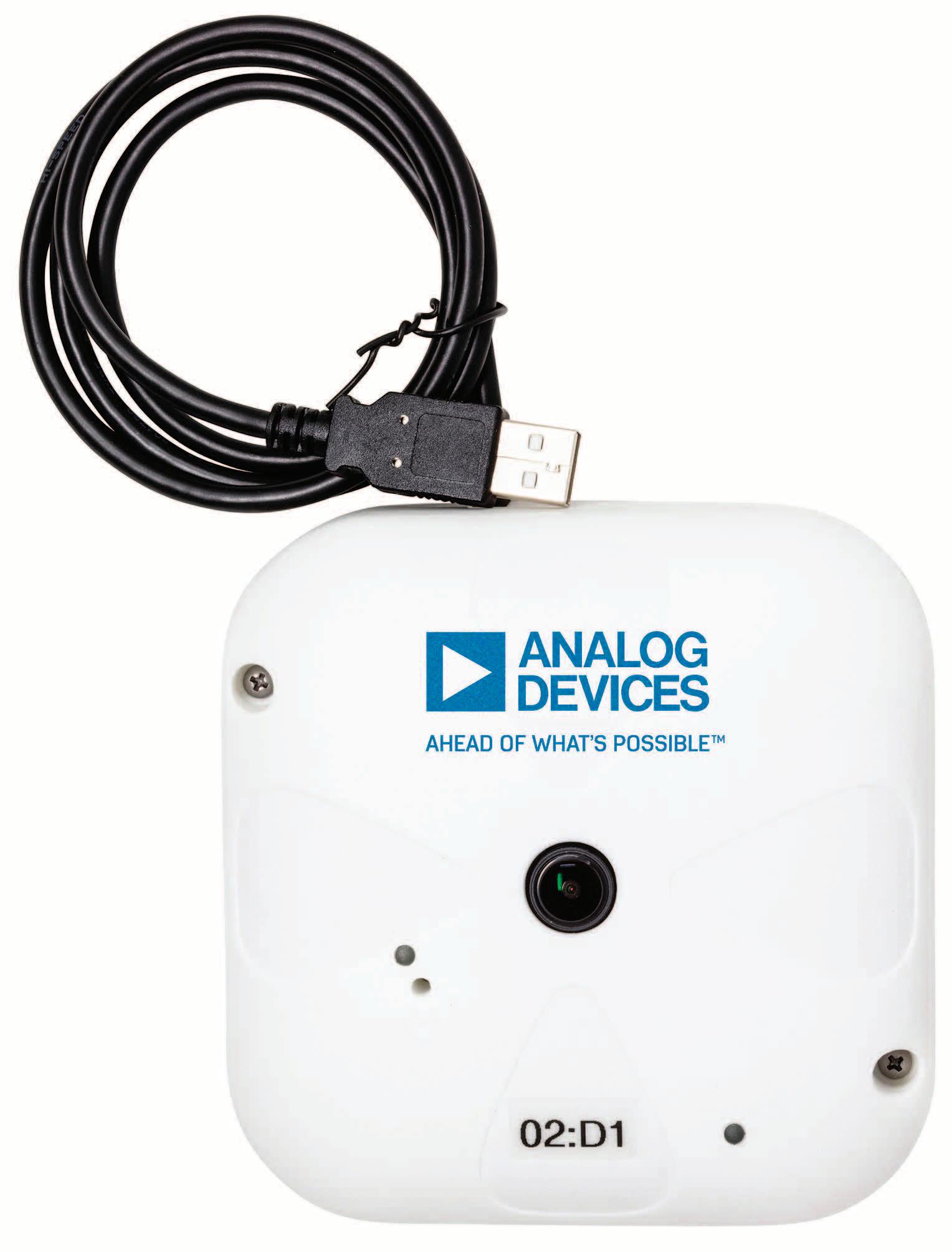
Analog Devices, Inc. (ADI) introduced the ADI Eagle Eye™ ADSW4000 People Count algorithm for people detection and count in indoor spaces such as meeting rooms or office cubicles. The ADSW4000 is the first in a series of application-level software algorithms forming part of the ADI EagleEye platform that includes a hardware subsystem based on ADI’s Blackfin® embedded digital signal processor (DSP) and a set of application-level software building blocks enabling users to quickly develop their own people counting system. The ADSW4000 algorithm provides system edge node analytics that unlock insights to improve space utilization, people safety through distance monitoring, and energy efficiency of spaces within intelligent buildings.
• Download the ADSW4000 data sheet and order the evaluation platform: https://www.analog.com/adsw4000
• Learn more about the benefits of ADI’s EagleEye platform: People Counting Technology Analog Devices or for more information contact: support@analog.com
• Watch a video about the ADSW4000 algorithm: https://www.analog.com/en/education/education-library/ videos/6277728474001.html
• Learn about more ADI intelligent building solutions: Intelligent Building Systems and Technologies | Analog Devices
• Connect with engineers and ADI product experts on EngineerZone™, an online technical support community: https://ez.analog.com
ADSW4000 Key Features:
• People counting algorithm for indoor areas, such as meeting rooms or office cubicles

- Occupancy state
- Location of person (x and y coordinates)
• Zoned performance (multiple areas for larger coverage)
• Edge processing
- Metadata output over UART
- No captured images are transmitted
• Coverage area for optimal accuracy of 90%: 3 m radius
• Maximum coverage area (accuracy of 80%): 5 m radius
The ADI EagleEye platform enables a complete, end-to-end hardware and software solution to help solve occupancy challenges. Combining the proprietary ADI ADSW4000 algorithm and advanced Blackfin DSP enables efficiency of indoor space while maintaining security and privacy as images are processed but not transmitted from the edge node. From meeting rooms to cafeterias, and lobbies to open desk people counting, ADI EagleEye can solve workspace needs and maximize worker wellbeing and productivity.
Analog Devices

https://www.analog.com
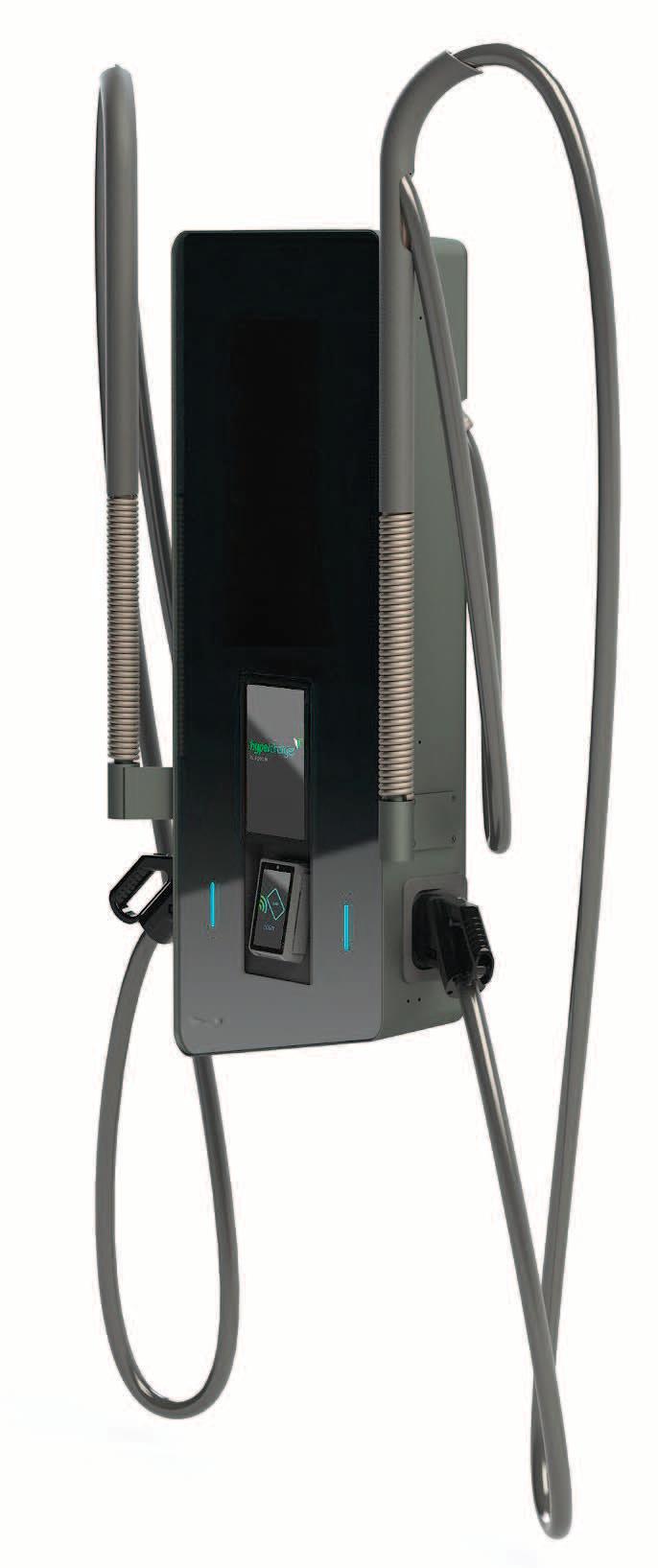
Following the successful launch of the HYC150 and HYC300 of their hypercharger product line, alpitronic recently introduced the state-of-the-art and industryleading 50 kW DC electric vehicle charger HYC50. It is the first wall-mounted DC charger in this power range featuring two charging ports that allow fast charging of one vehicle at 50 kW or of two vehicles simultaneously at 25 kW each. This is made possible by using EasyPACK™ CoolSiC TM MOSFET 1B and 2B modules from Infineon Technologies AG in combination with the EiceDRIVER™ X3.
“We are committed to working closely with customers like alpitronic to help them realize unique designs enabling superior system solutions,” said Dr. Peter Wawer, president of the Industrial Power Control Division at Infineon. “In addition to comprehensive system expertise and many years of experience, we offer first-class solutions such as our portfolio of EasyPACK 1B and 2B modules with the latest 1200 V CoolSiC MOSFET technology to increase the efficiency as well as the power density. The devices can be flexibly combined with suitable drivers to meet the requirements of each customer and their individual project.”
“With Infineon’s CoolSiC EasyPACK modules in combination with a perfect matching driver IC, we were able to significantly improve the efficiency of our new hypercharger,” said Philipp Senoner, co-founder and managing director of alpitronic. “We are therefore very pleased to have Infineon as a reliable and competent partner at our side, providing a wide range of CoolSiC MOSFET, gate drivers and the necessary understanding of our specific requirements.”
By using the CoolSiC technology, the HYC50 achieves up to 97 percent efficiency and enables a bidirectional design. As a result, this hypercharger is suitable for vehicle-to-grid (V2G) operation. At the same time, the charger has a compact footprint of 1250 × 520 × 220 mm3 and weighs less than 100 kg. Its compact size makes the charger ideal for indoor wall mounting, though it can also be mounted flexibly on a pedestal outdoors. The charger supports the charging standards CCS1 and CCS2 with a capacity of 150 A, CHAdeMO with a capacity of 125 A, as well as GBT.
In this particular design, Infineon’s EasyPACK 1B and 2B modules, which include CoolSiC MOSFETs, a NTC temperature sensor, and PressFIT contact pins, were able to increase
power density by about 50 percent. In addition, by using CoolSiC technology, the noise level was significantly reduced from 65 dB to less than 50 dB.
Besides the necessary power devices, Infineon also provided the matching drivers. The X3 driver IC is particularly suitable for the modules in this design, offering a number of decisive advantages through its configurability and active and passive monitoring options. For instance, it enables additional sensor points for operational monitoring, with several gate drivers providing additional temperature points as well as gate voltage monitoring. Thus, the temperature and voltage can be adjusted exactly according to the requirements of the SiC MOSFETs, minimizing static conduction losses and avoiding overloads. Furthermore, the operating points in the field can be optimized by OTA (Over-theAir) updates – these can also influence the parameters in the gate driver.
The EasyPACK CoolSiC MOSFET modules will be available in the first half of 2022.
Infineon Technologies
https://www.infineon.com

This article about Automotive Audio Bus® (A2B®) technology explains recent advances in digital microphone and connectivity technologies. These innovations are enabling swift adoption of game-changing applications for future generations of vehicle infotainment systems.
Within the automotive in-cabin electronics segment, it’s becoming increasingly clear that the universe of audio-, voice-, and acoustics-related applications is rapidly expanding as car manufacturers attempt to differentiate their vehicles from the competition. Additionally, as average consumers become more tech savvy, their expectations related to both the driving experience and level of personal interaction with the vehicle are expanding significantly. Home theater quality sound systems are commonplace across all vehicle price points and are now being augmented by sophisticated hands-free (HF) and incar communications (ICC) systems. Additionally, active and road noise cancellation (ANC/RNC) systems, historically deployed in only the top-level premium
vehicles, are now making their way into more mainstream, affordable segments. Looking to the future, audible or acousticsbased techniques will become a critical component in Level 4/Level 5 autonomous vehicle engine control units (ECUs) as they attempt to detect the presence of emergency vehicles.
The common thread binding all these legacy and emerging applications is the dependency on high performance acoustic sensing technology such as micro- phones and accelerometers. And since nearly all emerging applications require multiple acoustic sensors like microphones (or mic arrays) to achieve the best system-level performance, a simple cost-effective interconnect technology is required to ensure that total system costs
are minimized. Historically, the lack of a microphone-optimized interconnect technology has been a significant pain point for car manufacturers, as each microphone would need to be directly connected to the processing unit using expensive and heavy shielded analog cable. These added costs – primarily in terms of actual wiring, but secondarily in terms of added weight and reduced fuel efficiency – have in many cases prevented the widespread adoption of these applications, or at least limited them to only the super-premium segments. Recent advances in both digital microphone and connectivity technologies are proving to be enablers to the swift adoption of game- changing applications in future generations of vehicle infotainment systems. A2B technology will make a difference.
Using a handheld cell phone while operating a vehicle is banned in most countries, while Bluetooth®-enabled handsfree devices have become standard equipment in almost all vehicles. A wide array of hands-free solutions is available, from simple standalone units containing a loudspeaker and microphone to advanced solutions that are completely integrated within the vehicle infotainment system. Until recently, most hands-free systems were implemented in a very similar fashion. They were comprised of only one (rarely two) microphone(s), and the associated microphone technology was the 50-yearold electret condenser microphone (ECM) type. The voice quality of the transmitted audio was often unsatisfactory, especially in simple standalone units where the distance between the microphone and the talker’s mouth could be rather large.
Communication quality could be improved if the microphone were mounted as close to the mouth as possible (for example, in the headliner of the vehicle). However, in this case, both front seats require individual microphones if the driver and passenger are to be equally supported.
A typical automotive ECM is a device that combines the ECM capsule with a small amplifier circuit in a single housing. The amplifier delivers an analog signal with a voltage level that allows transport over wires of several meters in length, as required in typical automotive installations. Without amplification, the original ECM signal would be too low for such a wire length, as the signal-to-noise ratio (SNR) would degrade too far due to electromagnetic interferences on the wire.
Even the amplified signal requires shielded wiring, which is typically a 2-wire cable with a bias (8V) that supplies the microphone device. Given such wiring requirements, it is obvious that the number of ECM devices used in mainstream vehicles is limited due to weight and system cost constraints.
One of the few advantages of ECMs is their built-in acoustic directionality, which is usually trimmed to a super- or hypercardioid polar pattern (a MEMS mic can also be made unidirectional but typically requires more complex acoustic designs).
Typically, 10 dB or more backward attenuation can be achieved, where “backward” means the direction toward the windshield, from which only noise (that is, no desired signals, such as the talker’s voice) originates. Having a higher sensitivity in the incoming direction of the desired signal is very beneficial to increase the SNR.
However, directional ECM capsules introduce unwanted side effects such as the high-pass characteristic where sensitivity decreases at lower frequencies. The 3 dB cutoff frequency of such a high-pass response is typically in the range of 300 Hz to 350 Hz. In the early days of HF technology, this high-pass behavior was an advantage because engine noise was present primarily at lower frequencies, so the engine sound was already attenuated through the microphone.
However, since wideband, or HD, telephony is available, this high-pass behavior starts to become a problem. In a wideband call, the effective bandwidth is increased from 300 Hz to 3400 Hz, to 100 Hz to 7000 Hz. The built-in high-pass filter of the microphone makes it necessary to amplify signals between 100 Hz and 300 Hz in the postprocessing unit, which would not be required if the microphone were to deliver better audio bandwidth in the first place.
Another disadvantage of ECM technology is the significant part-to-part variation in terms of sensitivity and frequency response. The relatively large manufacturing tolerance of ECMs may not present a problem for single microphone applications.
However, if more than one microphone signal is deployed in a small-spaced microphone array application, then tight matching between microphones is essential for optimal array performance. In such a case, ECMs can hardly be used.
Furthermore, from the physical size perspective, traditional ECM capsules are not generally suitable for small form factor microphone arrays.
Microphone arrays have experienced widespread applicability including in vehicles because they can provide similar, often superior, directionality performance when compared to traditional ECMs.
Spatial information regarding sound impact directions can be extracted from the microphone signals using two or more suitable microphones grouped in an array. This class of algorithms is often referred to as beamforming (BF). The name beamforming is borrowed from an analogy with phased array antenna technology, where a radio “beam” is formed from the emission of an antenna array focused in a certain direction using a simple, purely linear filter and sum algorithm. Although there is no such beam in a microphone array, the term beamforming has also become very common in the field of microphone signal processing, where it covers a much wider range of both linear and nonlinear algorithms that enable higher performance and greater flexibility than the simple linear beamforming process.
In addition to the BF processing, a raw microphone signal almost always requires postprocessing because every HF microphone captures both desired voice signals and disturbances in the environment such as a car cabin. Wind, road, and engine noise deteriorate the SNR, and signals being played by loudspeakers – usually referred to as loudspeaker echoes – are additional sources of unwanted signals. In order to reduce such disturbances and improve voice quality, elaborate digital signal processing techniques are required, often referred to as acoustic echo cancelling and noise reduction (AEC/NR). AEC removes the loudspeaker sound from the microphone, which otherwise would be transmitted as an echo of the voice of the person speaking at the other end of the line. NR reduces constant driving noise while increasing the SNR of the transmitted signal.
Although elaborate specifications (for example, ITU-T P.1100 and P.1110) that define many performance details of an HF system have been published by the International Telecommunication Union (ITU), the subjective impression of the communication quality in a call from an operating vehicle can be unsatisfactory if the AEC/NR processing is of substandard quality. Together with the previously mentioned BF algorithm, the bundle of AEC/NR/BF enables a wide array of new applications, all related with some level of digital audio signal processing. To support these applications, a new generation of microphone technology overcoming disadvantages of traditional ECMs is demanded.
Microelectromechanical systems (MEMS) technology is swiftly becoming the new industry standard for microphones, as it offers many advantages over traditional ECMs. First and foremost, MEMS enable a much smaller form factor sound sensor than existing ECM capsules. Additionally, integrating a MEMS sensor with an analogto-digital converter (ADC) in a single IC results in a digital microphone that delivers signals ready for AEC/NR/BF processing.
Analog-ported MEMS microphones without an integrated ADC are also available, but they share many of the same disadvantages as analog ECMs and even require more complex amplifier circuitry than ECMs if operated on the traditional 2-wire analog interface. It is only with an all-digital interface technology that the interference and SNR problems inherent to analog wires can be significantly alleviated. Also, from a production perspective, MEMS are preferred because MEMS mics can be produced with a much tighter specification variance than ECM capsules, which is important for BF algorithms. Lastly, with MEMS IC microphones, the manufacturing process is greatly simplified because automated mounting techniques can be utilized, which reduces overall production costs. From an application perspective, the smaller form factor is the largest advantage, and, due to very small sound-entry portholes, MEMS mic arrays can be made virtually invisible. The porthole and the sound channel to the sensor require great care in terms of design and production quality.
If the acoustic seal is not tight, noise from the inner structure may reach the sensor and leakage between two sensors may degrade the performance of the BF algorithm. Different from typical ECM capsules that can be designed and manufactured to be either omnidirectional or directional, MEMS microphone elements are almost always manufactured to be omnidirectional (that is, they have no intrinsic directionality of sound reception). As such, MEMS microphones are phase-true omnidirectional sound pressure sensors that deliver ideal signals for advanced BF algorithms, where attenuation directions and beam widths can be user-configurable via software.
As a rule, it is very important that all signal processing modules are grouped in an integrated algorithm suite. Processing latencies would needlessly increase, and overall system performance would be degraded if functional blocks were implemented in isolation from one another.
For example, a BF algorithm should always be implemented together with the AEC and, optimally, from the same provider. If the BF algorithm introduces any nonlinear effects on the signal, the AEC will most certainly produce unsatisfactory results.
Ideal results of digital signal processing can best be achieved by an integrated algorithm bundle that receives uncorrupted microphone signals.
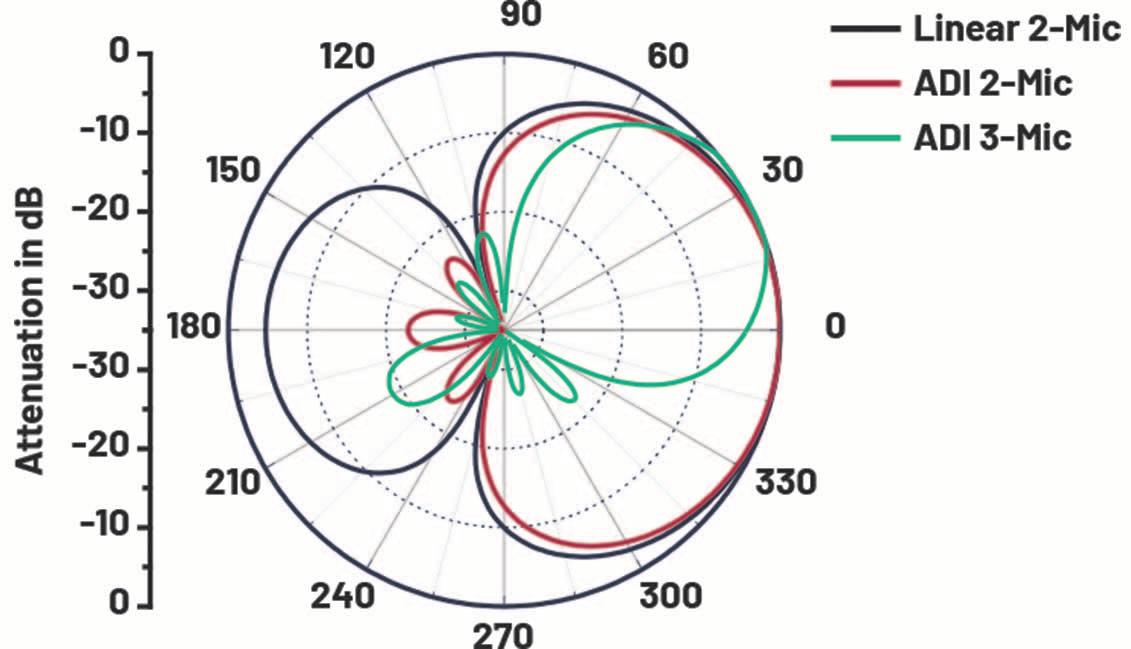
Standard linear BF and ADI-proprietary algorithms are compared below in detail in order to fully understand the performance potential of advanced BF algorithms. The plots in Figure 1 show three different BF algorithms regarding polar characteristics and frequency response in both in-beam and off-beam directions. A standard linear supercardioid algorithm based on a 2-mic array serves as the benchmark (black curves).
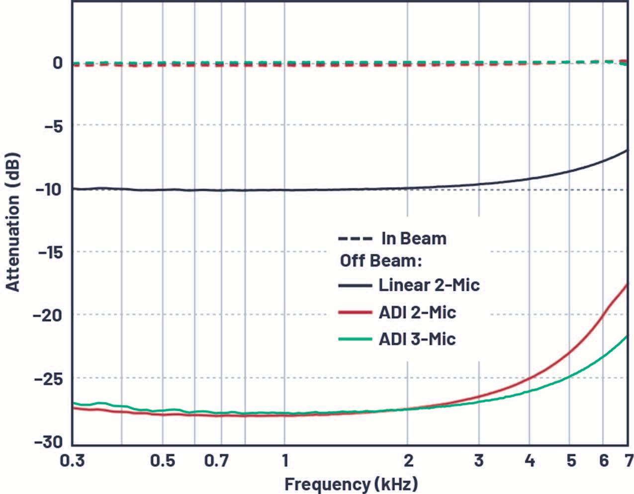
The benchmark curve shows the maximum attenuation in the typical zeroangle directions (that is, maximum offbeam attenuation) and a “rear-lobe” at 180°, where off-beam attenuation is lower. The resultant rear-lobe is a tradeoff with beam width in a linear algorithm. A cardioid beam (not shown) has its maximum attenuation exactly at 180°; however, its receptive area is broader than a hyper- or supercardioid configuration. Beams with less significant rear-lobes and higher off-beam attenuation can be achieved with nonlinear algorithmic approaches, with the red curve showing an ADI-proprietary 2-mic algorithm of this class (microphone spacing: 20 mm).
With two omnidirectional microphones in an array, there is always a rotational symmetry of the beam shape. In other words, the attenuation at X° in the polar plot is the same as at 360° – X°. This assumes that the 0° to 180° line of the polar plot is equivalent to the imaginary line connecting the two microphones. The 3-dimensional beam shape can be imagined by rotating the 2D polar plot around this microphone axis. Asymmetric beam shapes without rotational symmetry or more narrow beams require at least three microphones arranged in a triangle.
For example, in a typical overhead console installation, a 2-mic array can attenuate sound from the windshield. However, in such an orientation, a 2-mic array cannot distinguish driver from passenger. Rotating the array by 90° would make such driver/passenger distinction possible, but the noise from the windshield would not be distinguishable from sounds inside the cabin. Both windshield noise attenuation and driver/passenger differentiation are only possible using three or more omnidirectional microphones configured in an array. An exemplary polar characteristic of a respective ADI-proprietary 3-mic algorithm
is given by the green curve in Figure 1 where the microphones are arranged in an equal- sided triangle with 20 mm spacing.
Polar plots are computed with band-limited white noise arriving at the microphone array from different angles. The audio bandwidth is limited to 100 Hz to 7000 Hz, which is the wideband (or HDvoice) bandwidth of state-of-the art cell phone networks. Figure 2 compares the frequency response curves of the different algorithm types. In the in-beam direction, the frequency response of all algorithms is, as expected, flat within the desired audio bandwidth. The off-beam frequency responses are computed for the off-beam half-space (90° through 270°), confirming high off-beam attenuation over a wide frequency range.
The relationship between array microphone spacing and audio bandwidth vs. sample rate is worth further discussion. Wideband HD-voice uses a sample rate of 16 kHz, which is a good choice for speech transmission. There is a huge difference in voice quality and speech intelligibility between the current 16 kHz wideband sample rate and 8 kHz, which was used in earlier generations of narrow-band systems. Driven by speech recognition providers, there is growing demand for even higher sample rates, such as 24 kHz or 32 kHz. And specifications can be found where the sample rate of the voiceband application should be as high as 48 kHz, which is typically the primary system audio sample rate.
The underlying motivation is to avoid any internal sample rate conversion. However, the additional computational resources required to support these high sample rates cannot be justified by a tangible audible benefit, so 16 kHz or 24 kHz are now widely accepted as the recommended sample rates for most voiceband applications.
High sample rates are problematic for BF applications because spatial aliasing occurs at frequencies equaling the speed of sound divided by twice the microphone spacing. Spatial aliasing is undesirable because BF is not possible at such aliasing frequencies. Spatial aliasing can be avoided in a wideband system (16 kHz sample rate) if the microphone spacing is limited to 21 mm or less. Higher sample rates require smaller spacing to avoid spatial aliasing. However, overly small mic spacing is also undesirable because microphone tolerances and especially intrinsic (non-acoustic) noise of the microphone sensors can become an issue.
Signal differences between the microphones of an array get marginal if the spacing is small and disturbances such as intrinsic noise and sensitivity deviations between the microphones can overwhelm the signal difference between microphones. In practice, microphone spacing should not be less than 10 mm.
A 2B technology has been specifically developed to simplify the connectivity challenge in emerging automotive microphone and sensor-intensive applications. From an implementation standpoint, A2B is a single-main, multiple subnode (up to 10), line topology. The third generation of A2B transceivers that is currently in full production consists of five family members – all offered in automotive, industrial, and consumer temperature ranges. The full-featured AD2428W, together with four feature-reduced, lower cost derivatives –AD2429W, AD2427W, AD2426W, and AD2420W – comprise ADI’s latest family of pin-compatible, enhanced A2B transceivers.
The AD2427W and AD2426W offer reduced (subnode only) functionality and are primarily targeted for microphone connectivity applications such as hands-free, ANC/RNC, or ICC.
The AD2429W and AD2420W are entrylevel A2B derivatives that offer significant cost advantages relative to their full-featured counterparts and are particularly well-suited for cost-sensitive applications such as automotive eCall and multi-element microphone arrays. Table 1 shows a feature comparison among the thirdgeneration A2B transceivers.
The AD242x series supports daisy-chaining a single main plus up to 10 subnodes over a total bus distance of 40 m with up to 15 m supported between individual nodes. A2B’s daisy-chain, line topology is an important advantage over existing ring topologies as it relates to overall system integrity and robustness. If one connection of the A2B daisy chain is compromised, the entire network does not collapse. Only those nodes downstream from the faulty connection are impacted by the failure. And A2B’s embedded diagnostics can isolate the source of the failure, signaling an interrupt to initiate corrective action.
A 2B’s main/subnode line topology is inherently efficient when compared to existing digital bus architectures. After a simple bus discovery process, zero additional processor intervention is required to manage normal bus operation. As an added benefit of A2B’s unique architecture, system latency is completely deterministic (a 2-bus cycle delay, which is less
than 50 μs) irrespective of the audio node’s position on the A2B bus. This feature is extremely important for speech and audio applications such as ANC/RNC and ICC, where audio samples from multiple remote sensors must be processed in a time-aligned fashion.
All A2B transceivers deliver audio, control, clock, and power over a single, 2-wire, UTP cable. This reduces overall system cost for a variety of reasons.
• The number of physical wires is reduced relative to traditional implementations.
• The actual wires themselves can be lower cost, lower weight UTP as opposed to more expensive shielded cables.
• Jumper wires Most importantly, for particular use cases, A2B technology offers a bus power capability that delivers up to 300 mA of current to audio nodes on the A2B daisy chain. This bus power capability eliminates the need for local power supplies at the audio ECU – further reducing total system costs.
The total 50 Mbps bus bandwidth delivered by A2B technology supports up to 32 upstream and up to 32 downstream audio channels using standard audio sample rates (44.1 kHz, 48 kHz, etc.) and channel widths (16-, 24-bit). This pro- vides significant flexibility and connectivity to a wide range of audio I/O devices.
Maintaining a completely digital audio signal chain between audio ECUs ensures that the highest quality audio is preserved without introducing the potential for audio degradation via ADC/DAC conversion. System-level diagnostics are an essential component of A2B technology. All A2B nodes have the capability to identify a variety of fault conditions including opens, wires shorted together, reversed wires, or wires shorted to power or ground. This capability is important from a system integrity standpoint because, in the case of opens, wire shorts, or reversed wire faults, A2B nodes are still fully functional upstream of the fault. The diagnostic capability also provides for the efficient isolation of system-level failures, which is critically important from the dealer/installer standpoint.
The recently announced, fourth generation of A2B transceivers, AD243x, builds upon the existing technology foundation by increasing key functional parameters (node count increased to 17, bus power increased to 50 W) while adding an additional SPI-based control channel (10 Mbps) that provides an efficient software over-the-air (SOTA) capability for remote programming of intelligent A2B-connected nodes. The new features provided by the AD243x family make it well-suited for LED-fitted microphone nodes in superpremium microphone architectures.
From a single voice microphone to a multielement BF mic array for HF communication, from ANC to RNC, from ICC to siren sound detection, microphones have found more and more applications in the automotive industry. In accordance with the technology and market trend, almost every single new vehicle that hits the road today is equipped with at least one microphone module for HF communication. Premium and luxury cars may come with six or more microphone modules that are necessary for realizing the full potential of BF, AEC, ANC, RNC, ICC, and so on, where digital MEMS microphones present clear advantages. The growing microphone count presents one significant challenge to vehicle infotainment engineers - how to simplify the connecting harnesses and minimize their weight.
In the previously mentioned example, an HF microphone signal often prefers to have a rising frequency response shape (that is, sensitivity decreases with decreasing frequency) to remove the low frequency noise content inside the cabin. This is a helpful and very effective technique to improve the speech intelligibility delivered by a voice microphone.
On the contrary, an ANC microphone requires sufficient sensitivity level at low frequencies as the main purpose of the ANC algorithm is to reduce the low frequency noise. Thus, to share the same microphone in two applications in an analog system, the signal coming from the microphone needs to be fed into different circuits for proper frequency filtering. In this case, one or multiple ground loops may form, which can cause significant noise issues.
application block (HF, ANC, and BF) requires dedicated microphone(s) and separate harnesses for connecting to the corresponding functional circuit(s). This leads to four separate microphone elements and three sets of harnesses (a total of seven wires plus shielding). In contrast, because sharing signals is easily supported by the digital A2B system, the number of microphone elements can be potentially reduced from four to two. In this specific example, a single micro- phone module consisting of two wide bandwidth omnidirectional microphone elements can be used to provide two channels of acoustic signals that cover the needs of all application blocks. Once these two channels of signals reach the center processing unit (for example, the head unit or amplifier) through a simple UTP wire, they can then be shared and digitally processed to support HF, ANC, and BF applications.
This is not a trivial task for traditional analog systems. At a minimum, an analog microphone requires a pair of two shielded wires (ground and signal/ power), pins, and connector cavities for interconnection. The amount of wires is always twice the number of microphone modules in the system. Meanwhile, the total weight of the harness could increase even more rapidly depending on the wire length that is needed for connecting each microphone module. One simple way to mitigate this problem is to reduce the number of microphones used in the system by sharing a microphone signal among multiple applications. For example, the same microphone signal could be used in HF communications and as an error signal in the ANC system. However, different applications may require different microphone characteristics.
As a digital bus with daisy-chaining capability, A2B technology together with the digital MEMS microphone provide a wellsuited solution for interconnecting and/or sharing multiple microphone signals demanded by audio, voice, noise cancelling, and other acoustic applications that are rapidly expanding in vehicles. Consider an imaginary while exemplary case where a car application calls for an HF microphone module, an ANC microphone module, and a simple array microphone module consisting of two microphone elements for BF, and all three modules are integrated around the overhead console area. Figures 3a and 3b show how such a design may be realized with the traditional analog and the digital A2B systems, respectively. Since the analog system cannot easily accommodate microphone sharing, each
Although the example illustrated in Figure 3 may not represent a real situation, it clearly demonstrates the benefits of the A2B technology over the traditional analog technology. A digital audio bus system like the A2B technology addresses the challenge of automobile manufacturers to offer new audio and acoustic- related concepts that enhance user experience and allows these concepts to be brought to the market for faster implementation. Indeed, many applications that are either new to the automotive market or previously difficult to implement have been made possible by the commercialization of A2B technology. For example, as a leading automotive audio solution provider, Harman International has developed a family of digital microphone and sensor modules that takes advantage of the A2B system to enable various automotive applications.
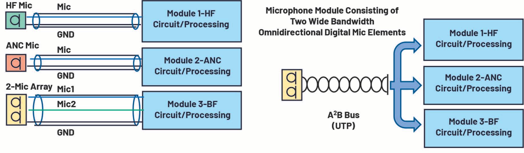
Figure 4 shows some common automotive A2B microphones and sensors and how they can be used on a vehicle. These sensors include single A2B microphones and multi-element microphone arrays for ANC and voice communication, A2B accelerometers for RNC, externally mounted bumper A2B microphones, and rooftop A2B microphone arrays for emergency siren detection and acoustic environment monitoring.
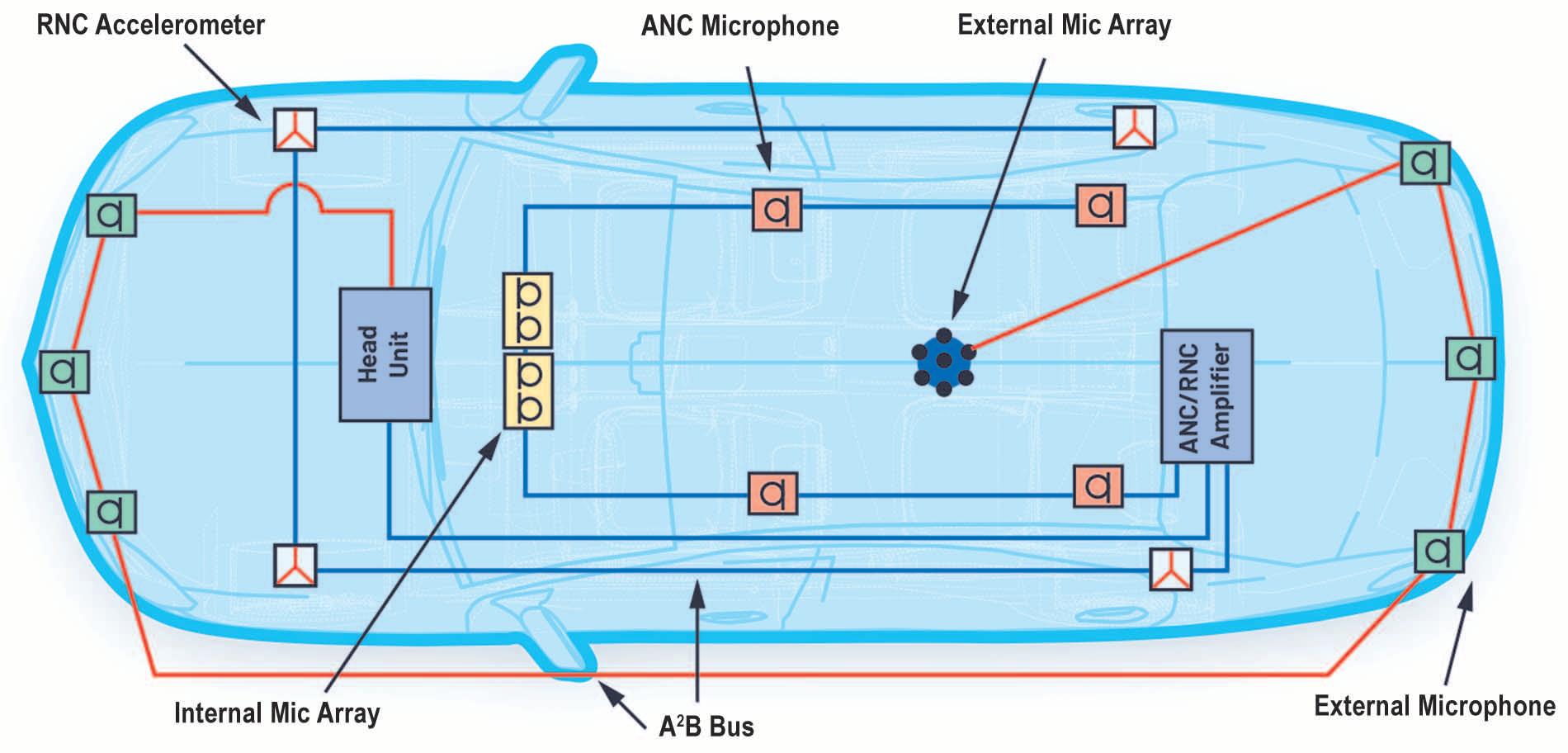
Enabled by these A2B microphones and accelerometers, more and more application solutions requiring multiple sensor inputs are currently under development to further enhance the user experience in the automotive industry.
Vehicle architectures of the future will become increasingly more dependent on


high performance acoustic sensing technology such as microphones and accelerometers. A completely digital approach including sensor, interconnect, and processor provides significant performance and system cost benefits. Analog Devices and Harman International are partnering to deliver cost-effective solutions that create value and differentiation for their end customers.
Analog Devices


https://www.analog.com
Visit https://ez.analog.com
About the authors
Contact Romania:
Email: inforomania@arroweurope.com
Mobil: +40 731 016 104
Arrow Electronics | https://www.arrow.com
Ken Waurin is a strategic marketing manager at Analog Devices, where he has overall responsibility for Automotive Audio Bus (A2B) technology. Since joining ADI in 1996, he has held product management, business development, tactical, and strategic marketing roles that span multiple technology areas including DSP, MEMS, converter, video, and connectivity. His primary focus is on automotive infotainment and emerging applications driving vehicle differentiation such as premium audio, road noise cancellation, and in-vehicle zonal communications. He can be reached at kenneth.waurin@analog.com
Dietmar Ruwisch is a senior audio technologist at Analog Devices. He studied physics in Münster, Germany, and received his doctorate in 1998 with a thesis on artificial neural networks. Since then his key area has been audio signal processing, where he holds several patents. His focus is on improving the quality of audio communication - whether between humans or with a machine - and the corresponding processing of microphone and microphone array signals. He can be reached at dietmar.ruwisch@analog.com
Yu Du is a senior principal acoustic engineer at Harman International Industries. He holds both a B.S. and M.S. degree in vehicle engi- neering from Tsinghua University (Beijing, China) and received his Ph.D. in mechanical engineering from Virginia Tech (Blacksburg, Virginia). His R&D experience extending over more than 20 years in various fields of acoustics includes structural acoustics, active and passive vibration and noise control, MEMS transducer design and simulation, hearing science, and acoustic signal processing. His current work at Harman focuses on advanced microphone and sensor technology development for automotive applications. Dr. Du is a member of The Acoustical Society of America (ASA), The Audio Engineering Society (AES), and The American Society of Mechanical Engineers (ASME). He currently serves on the AES Technical Committee for Automotive Audio.

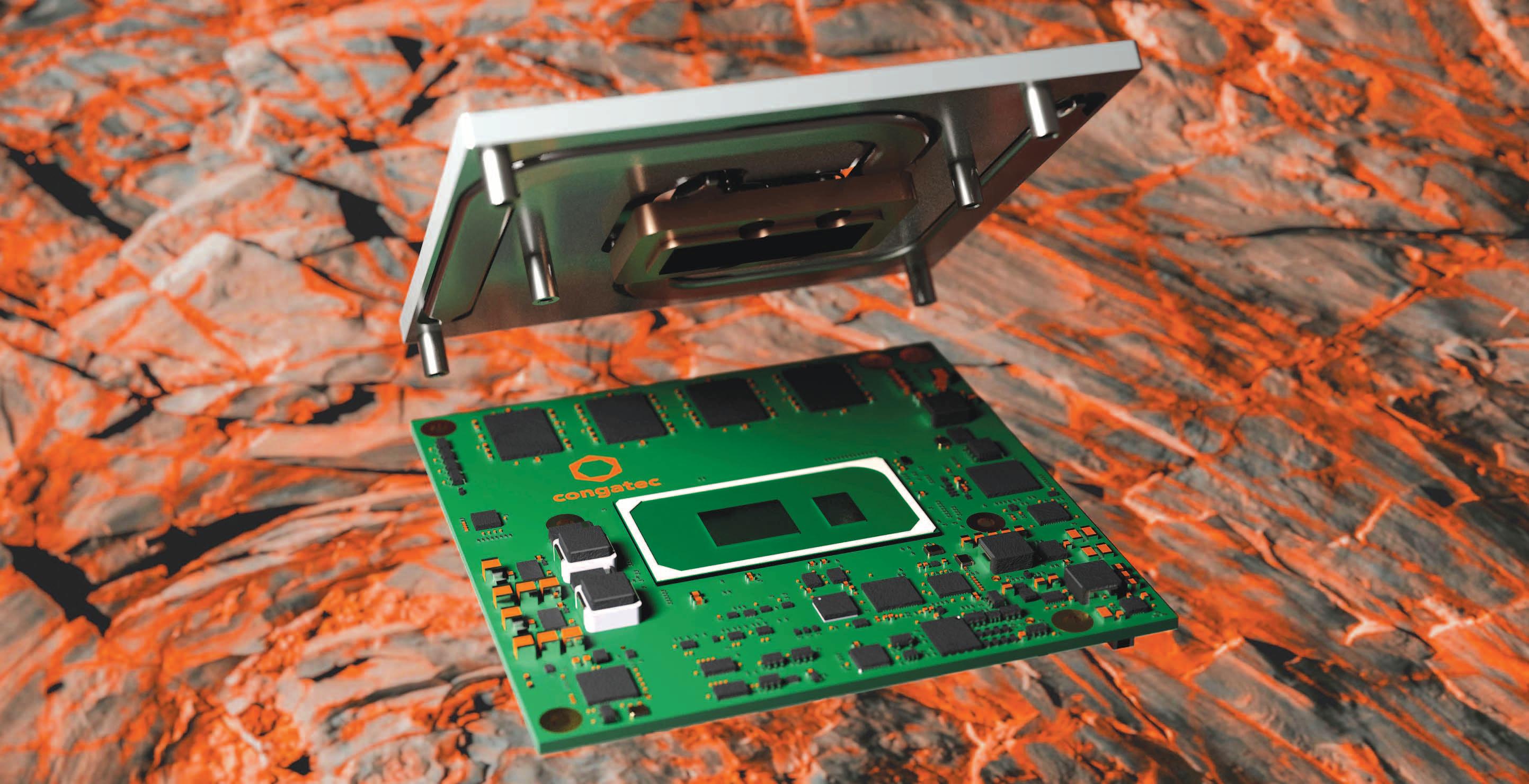
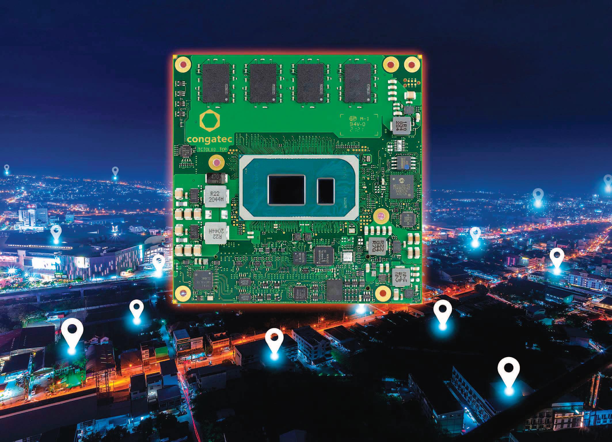
congatec COM

Express modules with 11th generation Intel Core processors are predestined for harsh environmental conditions

Most standard Computer-on-Modules use SO-DIMM connectors to integrate the main memory. Since the main memory is often customized for the specific application, this modular approach works well for module manufacturers and their OEM customers. However, the resistance of such connectors to shock and vibration is limited.
 Author: Zeljko Loncaric, Marketing Engineer

Although lever arm and mass are not so large, even comparatively small vibrations can impair the functional reliability of the RAM when standard memory modules are used. Applications exposed to high shock and vibrations therefore require more robust designs.
In the rail cargo sector, for example, vibrations of around 0.002 g2/Hz at frequencies from 0 to 350 Hz are common. Vibration levels experienced in jet aircraft are significantly higher at 0.01 g2/Hz with frequencies up to 2000 Hz. For systems deployed in trucks, levels even reach up
to 0.02 g2/Hz. And turbine engines, such as those used in wind turbines, pose higher demands still, stressing components with up to 0.03 g2/Hz.
Developers of such and many other mobile and stationary automation systems exposed to shock and vibration are therefore looking for better solutions to connect the main memory. For instance, memory manufacturers have added screw holes at the far end of their SO-
DIMMs to attach the RAM modules securely so that shock and vibration are no longer a problem.
But such technology does not have many takers that is why rugged SO-DIMMs with mounting holes have been mass-produced, which makes them more expensive. In addition, they are also more complex mechanically and hence more expensive to assemble. Lastly, they also require additional mounting holes on the boards, which further increases production costs. The best solution therefore is to avoid all these add-ons and simply solder the memory directly onto the module. This reduces the bill of materials for components, makes production more cost-effective and, most importantly, ensures ruggedness. And there is yet another distinct advantage of soldered memory: Cooling is easier than with conventional memory connectors. First, because the PCB on which it is soldered has better heat dissipation, and second, because the heat sinks of rugged Computer-on-Modules are specially designed for the respective ruggedness requirements and can be equipped with a heat-conducting connection for cooling hot spots such as the main memory.
congatec recently introduced new Computer-on-Module solutions based on the very latest 11th generation Intel Core processors with soldered RAM. These COM Express Type 6 Computer-on-Modules comply with the ETSI EN 300 019-1-7 and IEC 60721-3-7 specifications for portable and non-stationary telecom equipment and have been tested for commercial 7K3, 7M2 and industrial 7K4, 7M2 environments. This class also applies to nonweather protected locations in moderate outdoor climates and transfers between these conditions. For example, where equipment may be exposed to direct sunlight, radiant heat, ambient air movement, condensation, precipitation, and water from sources other than rain and ice.
In terms of shock and vibration, these modules are suitable for use in demanding transport and mobility applications up to offroad and rail vehicles. In addition they can withstand continuous operation in extreme temperatures (-40°C to +85°C), high humidity and heavy mechanical
stress due to shocks and vibrations and meet all requirements for fire protection. Typical customers for the new range of Computer-on-Modules based on the Tiger Lake microarchitecture are OEMs of trains, commercial vehicles, construction equipment, agricultural vehicles, self-driving robots and many other mobile applications in demanding outdoor and off-road environments. Shock and vibration resistant stationary devices are another important application area as digitization requires critical infrastructure protection (CIP) against earthquakes and other mission -critical events. All these applications can now benefit from super-fast LPDDR4X RAM with up to 4266 MT/s, which congatec offers in graded versions with 32, 16, 8 and 4 GB as standard variants. Depending on the requirements, the highest-performance modules can also be equipped with smaller memory or lower-performance variants based on the Intel Core i3-1115G4E with more than 8 GB RAM. In-band error correction code (IBECC) for single failure tolerance and high data transmission quality in EMIcritical environments corroborate the ruggedness of the modules.
The value package also includes rugged mounting options for the COM and carrier bundle, active and passive cooling options, optional conformal coating for protection against corrosion from moisture or condensation as well as sulfur protection, a list of recommended carrier board layouts and – for maximum reliability – shock and vibration resistant components for the extended temperature range. This impressive technical feature set is complemented by a comprehensive service offering that includes shock and vibration testing for custom system designs, temperature screening and high-speed signal compliance testing, as well as design-in services and all necessary training to simplify the use of congatec’s embedded computer technologies.
The Computer-on-Module concept in a nutshell: https://www.youtube.com/watch?v=2iPhK_nunJw&t=4s ►congatec
https://www.congatec.com
There has been an explosion in the number of Internet of Things (IoT) devices in the last decade, in markets ranging from medical devices to home and building automation to industrial automation. These are devices such as wearables, sensors, appliances and medical monitors – all connected, collecting and sharing massive amounts of data. A new forecast from International Data Corporation (IDC) estimates that there will be 41.6 billion connected IoT devices, or “things”, generating 79.4 zettabytes (ZB) of data in 2025.
Author: Kavita Char Renesas ElectronicsA key driver for this explosion in IoT is ubiquitous wireless connectivity that allows things to be connected to each other and to the internet. This hyper-connectivity has a lot of advantages such as automated control, easy communication between devices and sharing of data.
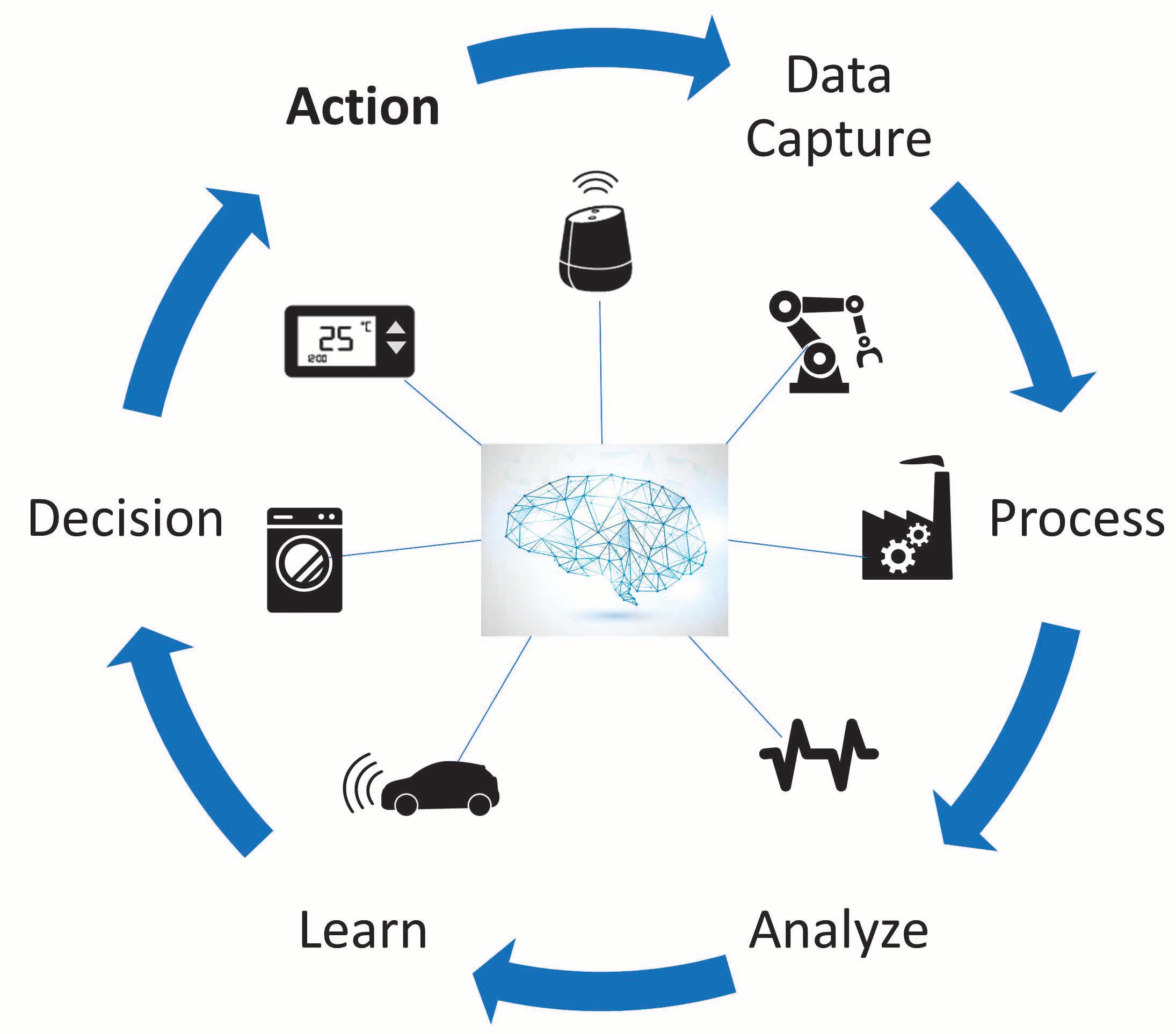
Elements of AIoT
It also allows collection and sharing of massive amounts of data that can be harvested and used to make intelligent decisions. As the number of connected devices grows, so does the amount of data that is generated. IDC forecasts that the amount of data generated by these devices will
see a compound annual growth rate of 28.7% over the 2018-2025 forecast period. Artificial Intelligence (AI) is the next logical step in making IoT even more useful. Intelligence can be built into IoT end devices to enable them to not only collect and share data but also to analyze it, learn from it and make decisions and act on it, without any human intervention. A combination of AI and IoT (AIoT) creates “intelligent” devices that learn from the generated data and use these insights to make autonomous decisions. New AI technologies are enabling intelligence on the edge and are significantly reducing the need for, and costs associated with cloud analytics. AI is expected to be the technology that helps IoT reach its fullest potential.
AIoT allows computation to move closer to the data. AI technologies, running on edge devices, can automatically process and analyze data generated by sensors and other IoT devices – such as temperature, pressure, humidity, vibration or sound – and use this information to make decisions and trigger actions.
In the past, AI applications have mainly run in the cloud due to complexity of the machine learning models. However, there are some applications that cannot run in the cloud due to lack of reliable and high bandwidth connectivity or when the application is such that it needs the models to be run at the device itself. These could be applications that need fast, realtime operation, which precludes the use of the cloud due to its latency. Examples of such applications are virtual assistants, industrial control, face recognition or medical devices that need quick real-time responses and cannot tolerate the latency of the cloud connection. Additionally, there might be concerns about security and privacy of data, driving the need to store and process data on the local device. Cloud connectivity and services can also be expensive and can drive up the cost of the devices or services associated with its use.

AI at the edge, therefore, provides advantages of autonomy, lower latency, lower power, lower requirement for bandwidth, lower costs and higher security, which make it more attractive for new emerging applications and use cases. Increased compute capability on the edge devices enables AI capability. AI finds use in many IoT applications such as vibration analysis, voice processing, image classification and computer vision, which need a combination of DSP compute capability and inference using machine learning.
1.The AI-enabled edge device market will be the fastest-growing segment within the AIoT
2.There is growing adoption of AI technologies in IoT end devices and companies are moving from cloud-based AI to edge AI to reduce latency and cost and enable real-time monitoring.
3.An analysis from Deloitte predicts sales of edge AI chips to exceed 1.5 billion units, representing annual unit sales growth of at least 20%.
AI in IoT offers a whole slew of benefits to users and organizations such as true intelligent automation, a richer user experience, deeper business insights and operational efficiencies.
Here are a few of these benefits:
AIoT can process and detect patterns in real-time operational data that are not
‘AI’ IN IoT - MARKET DRIVERS & TRENDS AIoT allows users to convert raw IoT data into useful insights that the system can learn from and that can drive decision making. MarketsandMarkets forecasts that the global AI in IoT market size will grow from USD 5.1 billion in 2019 to USD 16.2 billion by 2024, at a Compound Annual Growth Rate (CAGR) of 26.0% during the forecast period. According to MarketsandMarkets, the major factors expected to drive the market are the need to efficiently process huge volumes of real-time data being generated from IoT devices to gain valuable insights, real-time monitoring, enhanced user experience and reduced maintenance cost and downtime.
4 Gartner predicts that by 2022, more than 80 percent of enterprise IoT projects will include an AI component, up from only 10 percent today.
5.A lot of technology companies in the IoT space are investing significantly in AI in order to deliver new “intelligent” products, increase business efficiency and use data to drive business insights and enhance customer experience.
6.Venture capital funding and acquisitions of AI-focused IoT start-ups is growing fast.
7.Vendors of IoT platforms such as Amazon, IBM, Microsoft and Oracle, are integrating AI capabilities on their major general-purpose and industrial IoT platforms.
visible to the human eye and can use that data to set operating conditions in realtime, that result in optimal business outcomes. AI can thus help to optimize production processes and improve workflow resulting in increased efficiency and reduced operational costs.
AI can help institutions to use data to identify risks in a timely manner and use these insights to optimize their processes to increase safety and reduce loss and make better informed business decisions. Applications where AI can help to reduce risk include predicting mechanical faults on airlines and detecting safety risks on a factory floor.
AI and the ability to process and draw insights from large amounts of data, has opened up new technologies that did not previously exist such as voice recognition, face recognition and predictive analysis. These newly created capabilities can be used in many applications such as use of robots in delivery services or for disaster search and rescue operations, smart video doorbells, voice based virtual assistants and predictive maintenance for vehicles or building automation systems, amongst others.
In manufacturing, unplanned downtime of machinery resulting from equipment breakdown can be very disruptive to business. Predictive maintenance can help in predicting equipment failure by analyzing data from machinery and scheduling maintenance proactively, resulting in reduced incidence and costs of unplanned downtime.
AIoT enables new and advanced level of solutions that can transform businesses, enrich the user experience and increase safety and security. Here are some applications that benefit from AI:
Agricultural AIoT
Agriculture is one of the key segments that can benefit from AIoT.

Robots
Robots, in manufacturing as well as consumer products, are examples of applications that are very well suited for AI. Robotic vacuum cleaners have sensors that gather data on the environment and use AI to make decisions on how to traverse a space. Similarly, robots used in manufacturing, package/food delivery or search and rescue operations in disaster areas, use AI to sense complex (and sometimes hostile) environments and adapt their responses accordingly. Robots, with ability to recognize faces and human emotions, have also been used in retail environments to direct traffic and enrich the shopping experience.
Industrial automation
Computer vision with AI can be used to improve quality control on the assembly line and help with anomaly detection. AI can also help with predictive maintenance of the machinery to avoid downtime, improve machine life and reduce manufacturing costs. Robots can be used on the manufacturing floor or warehouses to move packages around, assist in the assembly line, inspect product quality and perform repetitive, high precision tasks.
In the retail environment, AIoT helps to tailor the shopping experience and provide personalized recommendations based on customer intelligence, demographic information and customer behavior.
By bringing analysis and decision making to the edge, AI helps to reduce volume of data that needs to be transferred to the cloud and hence reduce costs related to cloud connectivity and services.
AI is used to create an intelligent system that adjusts parameters based on weather conditions, water usage, temperature and crop/soil conditions. The data from sensors is analyzed to make optimal decisions on crop choices, fertilizers, irrigation and pest control. AI helps farmers in enhancing their yields, do seasonal forecasting and weather prediction for crop planning and utilizing resources in the most optimal way. Computer vision with AI is used to monitor crops and large farmlands to identify problem areas and generate alerts when needed.
Autonomous or self-driving vehicles combine IoT and AI to navigate through traffic, respond to changing traffic, weather or road conditions or predict the behavior of pedestrians. AI can also be used to gauge the condition of the vehicle based on collected usage data and provide predictive recommendations for maintenance.

AIoT can help companies to reduce their energy costs and make the buildings energy efficient by adjusting lighting and climate control based on building usage and user preference data.
Predictive maintenance (using diagnostic data on health of the building systems) allows repairs and maintenance when they are needed rather than on a schedule, thus helping companies save on costs. They can also provide alerts on potential system failures before they happen and help to tune the systems for optimal performance. AI can also be used for automated access control using camera sensors.
AIoT can open up new ways to create more efficient cities, maintain city infrastructure, and improve public services for communities. This can be done by gathering and analyzing data from multitudes of sensors and IoT devices and extracting actionable insights that can be used to make adjustments in real-time. Practical applications of AI include waste management, public services such as parking management, traffic management and smart lighting. As an example, drones can be used to monitor traffic in real-time and the data can be used to adjust traffic lights or lane assignments in order to manage and reduce traffic jams, all without intervention by humans. Similarly, sensors attached to waste bins can alert the operators to pick up the garbage only when the bins are full, thus helping to reduce costs.
AI finds application in fleet management by using predictive maintenance, with real-time monitoring of the fleet and proactive maintenance of the vehicles based on data collected from GPS trackers and sensors. AI also helps fleet operators with real-time navigation to reduce fuel costs, tracking vehicle maintenance, and identifying unsafe driver behavior.
AI can help retail in two ways. AI and predictive analytics help to collect and analyze large amounts of data and use that information to help retailers forecast and make accurate, data-driven business decisions. AIoT can use customer intelligence, demographic data and behavioral analytics to provide personalized recommendations to shoppers and improve store operations, product placement strategy, customer service and overall user experience. Retail robots can help to direct traffic and improve the customer experience.

AIoT in healthcare can be used for diverse applications, such as detecting and diagnosing diseases by analyzing imaging data, remote monitoring of patient’s information via sensors and raising alerts when anomalies are seen, predictions of a patient’s risk of diseases by analyzing EHRs (electronic health records) and predicting drug interactions. In addition, robotic surgical systems can perform or assist in very complex and high precision surgeries and make minimally invasive surgery possible.
It utilizes Deep Neural Network (DNN), a multilayered network that is particularly suited for applications involving image classification, voice recognition or natural language processing. The e-AI tools embedded in the Renesas e2 Studio Integrated Development Environment convert NN models into a form (C/C++ based) that is usable by the MCU and assist in embedding the pre-trained NN model on the target MCU.
‘AI’
AIoT is enabling new applications and use cases and will help IoT reach its fullest potential.
Renesas has a comprehensive family of Arm based MCUs capable of running AI applications. Renesas is working closely with ecosystem partners to bring end-toend AI solutions in predictive analytics, vision and voice applications, amongst others. Applications using these capabilities span market segments such as industrial automation, smart homes, building automation, healthcare and agriculture.
Renesas’s “e-AI” (embedded AI) solution uses the popular NN models - Caffe developed by UC Berkeley and TensorFlow from Google.
Applications of AIoT can be found in markets as diverse as smart cities, industrial automation, medical, agriculture and smart homes. We will continue to see a rise in new applications that will incorporate AI in IoT end points, and more and more manufacturers will make AIoT an area of significant investment.
►Renesas Electronics www.renesas.com

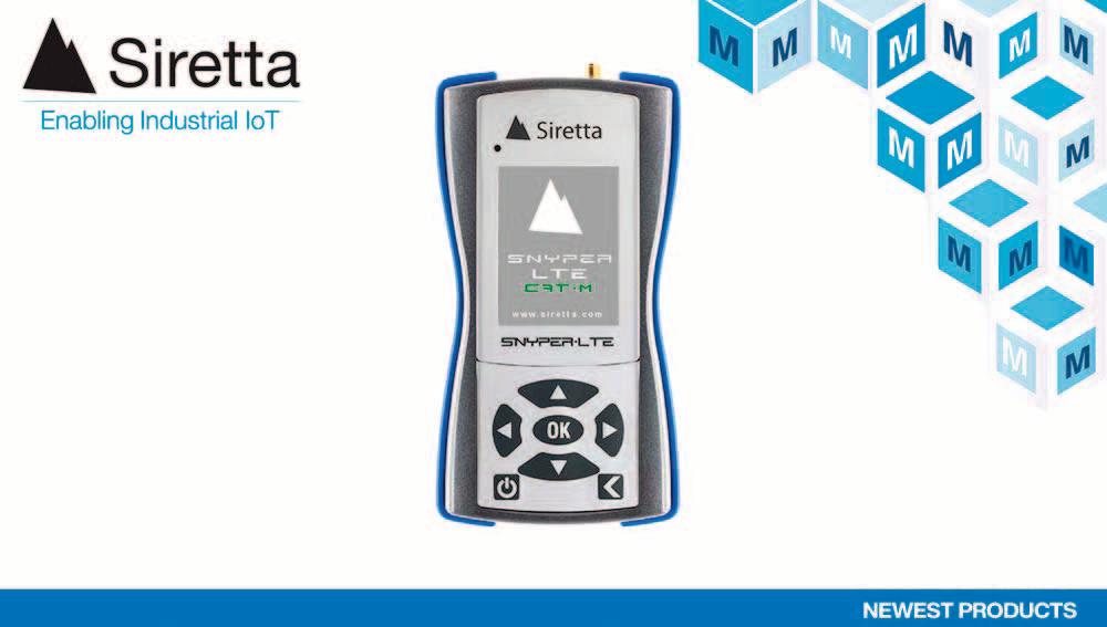
Mouser Electronics, Inc. announced it has entered into a global distribution agreement with Siretta, a leading global manufacturer and developer of Internet of Things (IoT) products, software, and complete end-to-end solutions. As part of the agreement, Mouser Electronics becomes an authorized distributor of Siretta’s advanced mobile broadband technologies, including its lines of SNYPER network signal analysers, high-speed QUARTZ industrial routers, and ZETA modem starter kits - all designed for a variety of IoT, industrial, and transportation applications.
The Siretta SNYPER-LTEM (GL), now available from Mouser Electronics, is a high-performance, multi-language network signal analyser dedicated to surveying LTE Cat M, LTE Cat NB IoT, and 2G/GSM Global networks. The powerful SNYPER summary page displays percentage thresholds to determine the most suitable mobile network operator (MNO) available and the performance of a “preferred” MNO can be evaluated against the other networks.
Siretta’s high-speed EU industrial routers include the QUARTZ-LTE dual-port LTE routers (EU) and the QUARTZCOMPACT single-port 4G/LTE routers (EU), which enable industrial IoT applications to transfer large amounts of data over a cellular network. Both routers offer upload speeds up to 50 Mbps, with fallback to 3G/UMTS or 3G communication (respectively), should 4G/LTE be unavailable.
The QUARTZ-LTE router enables fast downloads up to 100 Mbps, with dual SIM backup, dual-port Ethernet capabilities, and Wi-Fi or GNSS asset tracking/management options. The QUARTZ-COMPACT router offers download speeds of up to 150 Mbps, a single SIM slot, 10/100 Ethernet LAN port and serial port for serial-to-IP transfers, which can be swapped out for an optional GPS. Both routers contain QUARTZ software (which offers support for VPN security) and function across the European (EU) 4G/LTE bands. The routers provide a robust industrial design and strong resistance to EMI and are ideal for applications requiring local or remote communications.
The ZETA family of modems connect equipment to the LTE Cat 4, LTE Cat 1, LTE Cat M, and LTE Cat NBIoT networks and provide backward compatibility to the existing 3G/UMTS and 2G/GSM cellular networks.
►Mouser Electronics | https://www.mouser.com
Infineon Technologies launched the company’s fifth-generation CAPSENSE™ capacitive and inductive touch sensing human-machine interface (HMI) technology. The next-generation CAPSENSE solution embedded in PSoC™ microcontrollers delivers higher performance and lower power consumption for demanding user interfaces in home appliance, industrial, consumer and IoT products. The enhanced HMI enables advanced solutions like proximity sensing with improved detection range, gesture detection and directivity, along with hover detection for tomorrow’s advanced touchscreens.
With ten times better performance and a tenth of the power consumption of previous generations, the new CAPSENSE technology allows designers to develop more intuitive user interfaces, while significantly reducing overall power consumption to meet the demands of battery-powered IoT devices. The latest CAPSENSE generation is ideal for home appliance and industrial applications including smart door locks, smart switches, thermostats, smart speakers, power tools, industrial touchscreens and other IoT devices. The new technology is also ideal for applications with larger touchscreens in industrial and home appliance products including induction cooktops, washer and dryers, refrigerators, ovens and more.
“As the leader in capacitive touch sensing technology nearing four billion units sold, we are excited to offer our fifth generation CAPSENSE technology to designers,” said Steve Tateosian, Vice President of IoT Compute and Wireless Business Unit of Infineon. “This new generation of CAPSENSE technology builds
Infineon’s 5th Generation CAPSENSE™ technology extends market leader-ship with improved robustness, reliability and lower power consumption
on our established leadership with an all-new ratiometric and differential sensing architecture. It provides improved noise immunity, and a robust and reliable HMI solution to perform even in the harshest environments with extreme electrical noises, and under extreme weather and temperature.”
Infineon’s proprietary CAPSENSE technology empowers designers to develop more advanced HMIs on tomorrow’s devices with various touch sensing user interface requirements. With the ultra-low power capabilities and the ability to fit in smaller form factors, this technology is also ideal for touch interfaces on wearables, hearables and smart IoT applications. The new CAPSENSE technology enables advanced HMI solutions like proximity sensing with improved detection range, gesture detection and directivity. A new, autonomous sensing mode, enables operation without a CPU reducing power consumption and a new ratiometric sensing architecture and differential signal path improves noise immunity and performance.
With Infineon’s CAPSENSE capacitive touch sensor interface, a user’s finger on the interface forms an electrical connection with embedded sensors. The sensors work with the PSoC device to translate data about the finger’s position into various system control functions. A single PSoC device can replace dozens of mechanical switches and controls with simple, touch-sensitive controls. CAPSENSE-based “button” and slider controls are more reliable than their mechanical counterparts because they are not prone to the environmental wear-and-tear that affects exposed buttons and switches. More information is available at: https://www.cypress.com/products/capsense-controllers.
Infineon’s fifth generation CAPSENSE capacitive sensing HMI technology embedded in PSoC 4 devices is available to lead customers today including support in ModusToolbox™. More information: https://www.cypress.com/products/capsense.

►Infineon Technologies | https://www.infineon.com


Analog Devices, Inc. announced a breakthrough RadioVerse® System-on-Chip (SoC) series providing radio unit (RU) developers with an agile and cost-effective platform to create the most energy efficient 5G RUs in the industry. The new SoC series provides advanced RF signal processing with expanded digital functionality and RF capacity that greatly improves 5G RU performance and energy efficiency. The SoCs are the newest addition to ADI’s RadioVerse ecosystem and combine its award-winning Zero IF (ZiF) architecture with significant advances in functional integration and linearization. ADI’s RadioVerse devices are the most widely used softwaredefined transceivers in 4G and 5G RUs worldwide.1
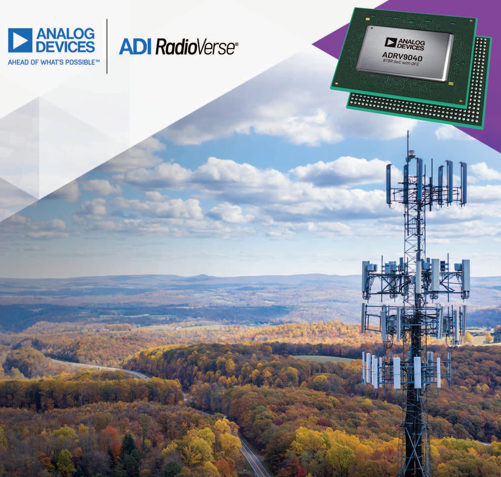
Demand for power efficient RUs is expanding rapidly as global network operators race to deploy 5G infrastructure. With the exponential growth of wireless demand, energy efficiency is a key metric for operators as they seek to reduce their carbon footprint while expanding network capacity. The new RadioVerse SoC series requires very low power compared to alternatives and implements advanced algorithms that deliver optimal RU system efficiency.
The ADRV9040 is the first in the new RadioVerse SoC series. It offers eight transmit and receive channels of 400MHz bandwidth and integrates advanced digital signal processing functions, including carrier digital up-converters (CDUC), carrier digital down-converters (CDDC), crest factor reduction (CFR) and digital pre-distortion (DPD). This expanded signal processing can eliminate the need for a field-programmable gate array (FPGA), thereby reducing thermal footprint, and total system size, weight, power, and cost. The SoC’s DPD algorithms were developed using advanced machine learning techniques and are optimized in close collaboration with major power amplifier (PA) vendors to ease the design burden and deliver best-inclass wide bandwidth performance. The algorithms are fully tested and validated across 4G and 5G use cases, including various PA technology types such as gallium nitride (GaN). In addition, the ZiF radio architecture simplifies RF filtering and signal chain components, reducing RU cost and development time for band and power variants designs.
Learn more about the ADRV9040 RadioVerse SoC at https://www.analog.com/ADRV9040
►Analog Devices | https://www.analog.com

Security is now a key requirement for embedded systems. The desire to connect devices to the internet to make it easier to control them and pull live data from their sensors brings with it a high risk of hacking. The hacking activity does not put at risk just individual devices but entire networks.
Author: Nicolas Demoulin, EMEA Marketing Manager – Secure Products Group

The direction is clear: vendors cannot go to market without an IoT product secure by design. The issue for device manufacturers as they look to harness the power of the IoT for their systems is the complexity of implementing effective and relevant security mechanisms. It is easy to see the fundamental need for authentication and encryption in these systems. But implementation has been much harder to achieve. There are multiple components, both software and hardware, that are needed to create a secure foundation for an embedded system.
A weakness in any one of them can easily lead to the hardware being compromised and loaded with malware that is used to attack an operator’s network or to leak sensitive data to cybercriminals. At the same time, many design teams are confronting for the first time the development difficulties presented by security concerns.
One of the core requirements for effective security is that each deployed device should have its own unique identity. A common flaw exploited by hackers is to have devices provide a common password or login for use by service and maintenance engineers.
The details of this login are often easy to guess and even if they are not they are usually easily obtained by a hacker. With this login, it is possible to gain access to not just one device but the entire fleet. Cybercriminals were able to create botnets – armies of identical computers used in denial-of-service attacks – through the use of simple automated scripts. The scripts identified and logged into each device of a certain type that had an internet connection.
With a unique identity, it is possible to give each system its own security credentials and greatly reduce the chance of giving hackers an easy way to construct botnets. Only if an authorized user has the right credentials for a particular device should they be allowed access. However, this increased level of protection has ramifications for the design, development and service management processes. Implementing effective security in a way that facilitates rather than impedes development involves careful choices. The first choice is over the hardware foundations employed to protect the integrity of the target device.
This foundation ensures that it is impossible not just to access the core firmware of the device without authorization but to ensure its functions cannot be subverted and the device used to attack the network. For example, if a hacker has obtained access credentials for one device, it must be impossible to convert another to accept those same credentials in order to form, for example, a botnet. As a result, identity and integrity are intimately tied.
The public-key infrastructure (PKI) provides a means for establishing and proving a unique trusted identity not only within the device itself but across a network. PKI relies on the concept of asymmetric cryptography, a technique that links two numeric keys together mathematically. One is a public key, which is typically used to verify messages. As its name suggests, this key can be distributed widely without compromising security. And it provides an easy way for anyone to send secure messages to a device, just as long as they know which public key to use. The device itself needs the private key which allows to sign messages sent to it which will be verified by the corresponding public key.
From the basic PKI operations, it is possible to construct more structured authentication models, such as digital certificates that demonstrate the identity of a device. To create a digital certificate, a device signs a message or challenge creating a signature using the private key. The corresponding public key is used by the recipient to determine the validity of the signature.
The private key clearly needs strong protection. It is not enough to just program a key into non-volatile memory on a device before it is deployed as it’s easily accessible. The private key should never be disclosed. If there is a disclosure, it is possible for hackers to build their own clone devices. These are then able to impersonate and spoof the authentic device and so compromise the security of networked applications which depend on the data sent by the device.
A problem for a conventional microcontroller-based design is that any cryptographic software running on the processor core needs access to the private key in order to perform the necessary calculations assuming the key is in the controller. The core hardware requirement therefore is a secure element used to fold those cryp-
tographic operations into a standalone piece of protected hardware together with secure storage for the private keys. As the key and cryptographic functions stored together inside the same physical secure boundary, there is no need to send sensitive data over the system’s internal bus.
This key used to verify the code signature is a sensitive credential that will and so should live in a protected and immutable memory zone. If the key can be altered, the system would simply not work. If the key pair can be altered then the code can similarly be tampered with.
Instead, when the system needs to communicate securely or prove its identity, it calls upon the secure element to respond to a random challenge. The response to this challenge is a code derived arithmetically from the random part of the challenge and the relevant private key stored inside the secure element. In other words, the random challenge is signed by the private key. In this way, the secure element can demonstrate that it holds the appropriate secret but does not need to disclose the sensitive private key itself.
The secure element can also protect the device from counterfeit code that an attacker might attempt to run and use to try to compromise the system. The protection mechanism that is needed to prevent this is a code verification, sometimes known as a secured boot or a runtime code verification. In this case, the challenge sent to the secure element is a signature obtained from the signed boot image stored on the device. Any updates to the code have to be signed by the OEM using its private key. Through secured boot and runtime verification procedures, the system can support over-the-air updates provided by the manufacturer without the risk of running updates provided by a third party using a man-in-themiddle attack or a similar approach.
An example of effective protection can be found in the Microchip Technology ATECC608A. This is a secure element that can be used with in any microcontrollerbased system thanks to its use of a standard I2C or Single-wire communication link. The device combines a non-volatile memory with several crypto-accelerators designed to support algorithms based on elliptic-curve algorithms, for example, in a secure silicon. The device never reveals private keys through the communication link and includes a number of anti-tampering hardware features that make it practically not feasible to discover its contents.
Although a secure element coupled to a microcontroller provides an effective foundation for building connected embedded devices that can guarantee high security, this combination is only part of the overall solution. There are many use-cases that involve constructing complex protocols in embedded software out of the core functions a secure element provides.
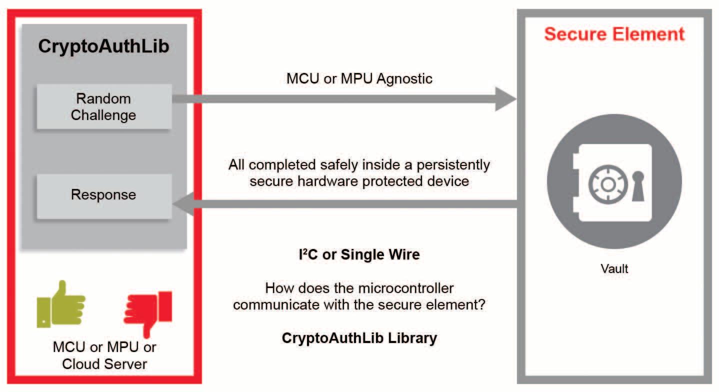
For example, in addition to secure boot, an IoT device will need to be able to communicate with remote hosts using encrypted protocols such as TLS and generate certificates on demand that show that the device has not been compromised when it wants to connect to a new service.
When the manufacturer or service operator wants to send a code update, that firmware’s signature will need to be verified before the flash memory is updated and the system rebooted.
A further requirement may be the ability to detect system accessories or consumable cartridges and determine whether they are authentic. This function can be performed using protocols that are similar to those used to build the code verification example, but with some key differences. For example, each peripheral may have its own secure element that is used to check that the host system into which it is plugged is itself authentic.
Although the principles behind each of the protocols that implements these functions are reasonably straightforward, implementation can be difficult because the ability to debug problems is constrained by the need for the system to obey the secure protocols.
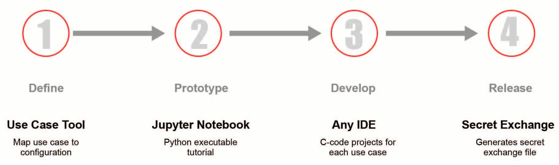
A common assumption during development is that pressing the reset button or flushing the contents of memory will let engineers gain access to an unresponsive device. Debug modes generally give the developer privileged access to the system. But when the higher levels of security required for systems that will be connected to the internet are introduced, some of these assumptions no longer apply. Failure to implement software in the right way can lead to the prototype device becoming unreachable. The most troublesome parts of secure-system development lie in the debugging of the core protocols. For example, it is easy to introduce bugs into the code used to process passcodes or security certificate that cause the device to be unable to respond to valid requests. If it were possible to reset the device to gain access, the facility would provide hackers with an easily exploitable backdoor into the system. As a result, security-focused development introduces hurdles into the development process. They are difficult to deal with if the team does not have experience of the techniques that are required.
However, one advantage of systems built on a PKI infrastructure is that applications can be built on top of core protocols and use-cases, such as the verification of signed executables and certificate creation, that can be reused across many projects. Such insight helped lead to the creation of Microchip’s Trust Platform.
This platform provides a suite of configurations, source code, hardware and software tools designed to make it easy for customers to implement a wide variety of use-cases in a workflow that guides the user from concept to implementation based on hardware that includes a secure element such as the ATECC608A. The Trust Platform divides into three main offerings. The simplest is Trust&GO, which provides a fixed set of functions, such as giving a device access to cloud services hosted on AWS, Google Cloud, Microsoft Azure or a private cloud. Another configuration supported by Trust&GO is a complete secure authentication solution for devices that need to connect to a LoRaWAN wireless network.
With competing secure-element supply chains, the minimum order quantity can be 100,000 because of the overhead involved in setting up the initial certificates and keys that need to be programmed into the hardware in the supplier’s secure manufacturing production line. With Trust&GO, customers can buy secure elements starting 10 units per order and have all the support of the Trust Platform infrastructure, including provisioning. For TrustFLEX, the minimum order quantity is as low as 2,000 units also including provisioning, but still provides the user with the greater level of control over certificates, keys and applications that might be expected from customized secure supply-chain solutions.
TrustFLEX provides an additional level of customization with support for a wide range of operations from secure boot to certificate generation. The third option, TrustCUSTOM, provides customers with the ability to tune the creation and integration of secure elements into their desired security model.
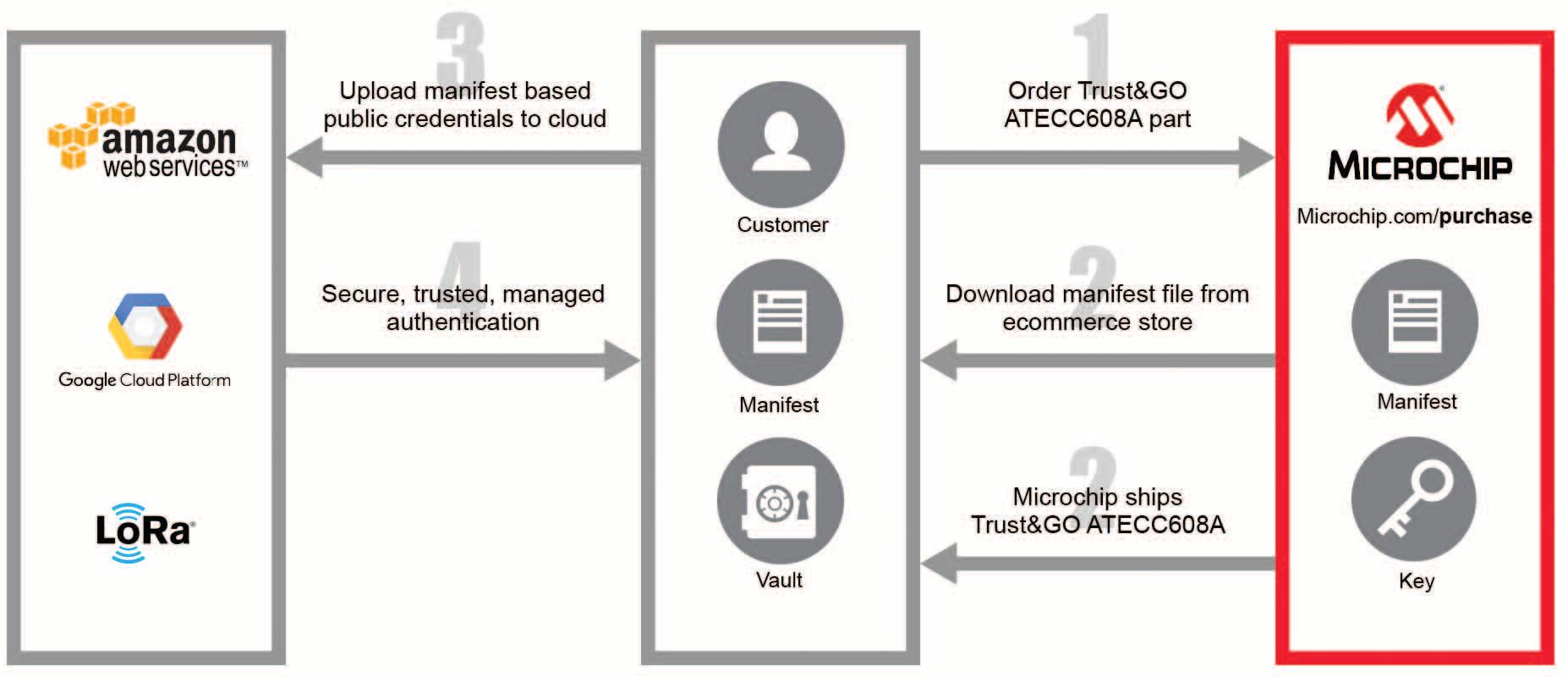
An important element of the Trust Platform that eases access to security compared to other offerings is the way in which the secure key provisioning service can be deployed on low-volume applications.
Under the Microchip Trust Platform, customers have access to highly customizable security mechanisms with much lower development and deployment risk than existing solutions. The combination of tools, source code and supply infrastructure provide a path for embedded systems developers to gain access to a complete securely provisioned system that works from concept to deployment, reducing the development process from months to days.
►Microchip Technology https://www.microchip.com

New Monolithic Microwave Integrated Circuits (MMICs) and discrete devices deliver performance levels required in 5G, satellite communication and defense applications
Microchip Technology Inc. announced a significant expansion of its Gallium Nitride (GaN) Radio Frequency (RF) power device portfolio with new MMICs and discrete transistors that cover frequencies up to 20 gigahertz (GHz). The devices combine high power-added efficiency (PAE) and high linearity to deliver new levels of performance in applications ranging from 5G to electronic warfare, satellite communications, commercial and defense radar systems and test equipment.
Like all Microchip GaN RF power products, the devices are fabricated using GaN-on-silicon carbide technology that provides the best combination of highpower density and yield, as well as highvoltage operation and longevity of more than 1 million hours at a 255o C junction temperature.
They include GaN MMICs covering 2 to 18 GHz, 12 to 20 GHz, and 12 to 20 GHz with 3 dB Compression Point (P3dB) RF output power up to 20 W and efficiency up to 25%, as well as bare die and packaged GaN MMIC amplifiers for S- and X-band with up to 60% PAE, and discrete high
electron mobility transistor (HEMT) devices covering DC to 14 GHz with P3dB RF output power up to 100W and maximum efficiency of 70%.
“Microchip continues to invest in our family of GaN RF products to support every application at all frequencies from microwave through millimeter wavelengths, and our product portfolio includes more than 50 devices, from low-power levels to 2.2 kW,” said Leon Gross, vice president of Microchip’s discrete products business unit “Together the products announced today span 2 to 20 GHz and are designed to meet the linearity and efficiency challenges posed by the higher-order modulation techniques employed in 5G and other wireless networks, as well as the unique needs of satellite communications and defense applications.”
Microchip’s portfolio of RF semiconductors in addition to GaN devices ranges from gallium arsenide (GaAs) RF amplifiers and modules to low-noise amplifiers, front-end modules (RFFEs), varactor, Schottky, and PIN diodes, RF switches and voltage variable attenuators.
In addition, the company provides highperformance surface acoustic wave (SAW) sensors and microelectromechanical systems (MEMS) oscillators and highly integrated modules that combine microcontrollers (MCUs) with RF transceivers (Wi-Fi® MCUs) that support major shortrange wireless communications protocols from Bluetooth® and Wi-Fi to LoRa®.
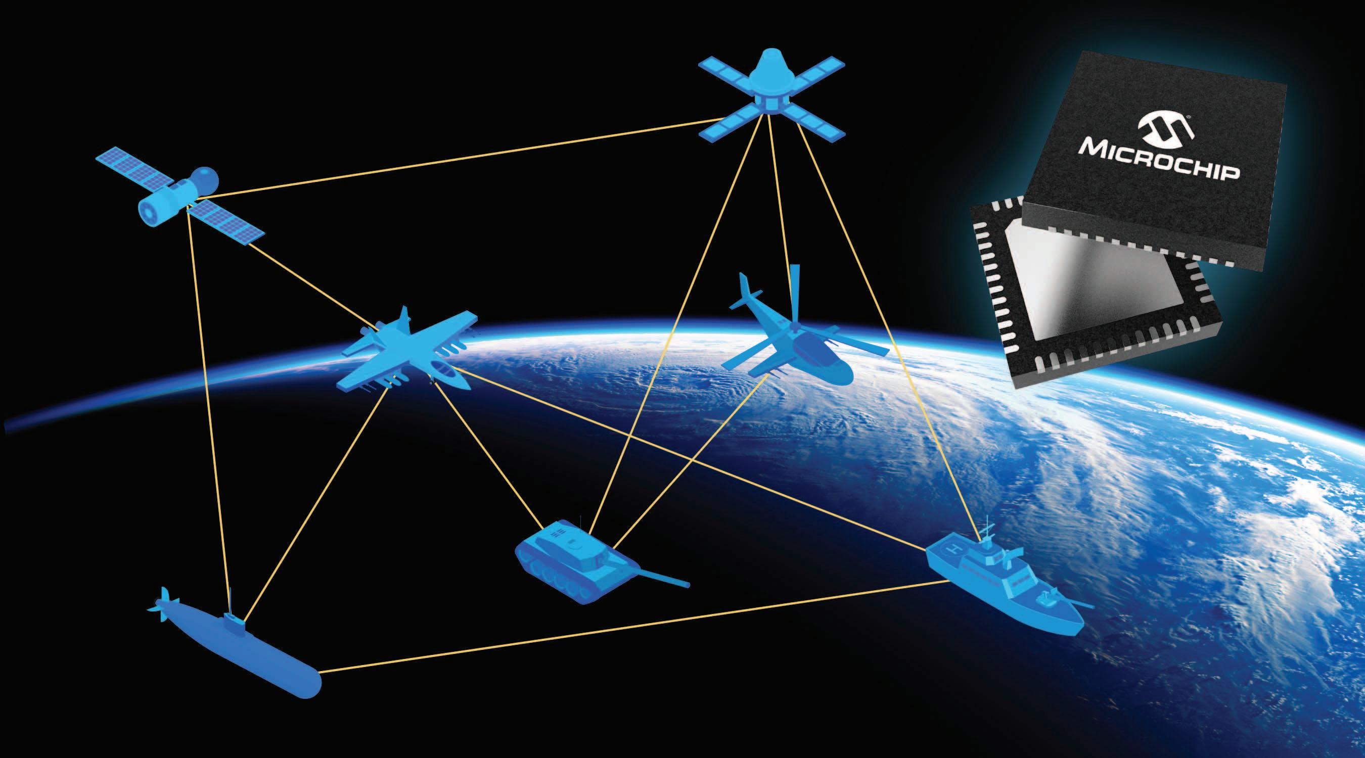
Microchip provides board design support to help with design-ins, as do the company’s distribution partners. The company also provides compact models for the new GaN products that let customers more easily model performance and expedite the design of the power amplifiers in their systems.
The power devices announced today, include the ICP0349PP7-1-300I and ICP1543-1-110I, as well as other Microchip RF products, and are available in volume production. For additional information, contact a Microchip sales representative or visit Microchip’s website. To purchase Microchip’s GaN products, contact a Microchip authorized distributor.
Microchip Technology
https://www.microchip.com
In recent years, there has been an explosion in the numbers of connected IoT devices in markets as diverse as industrial automation, smart homes, building automation and wearables. These connected devices, or “things”, share one common trait – they all communicate with each other and share data generated by multiple sensors. A new forecast from International Data Corporation estimates that there will be 41.6 billion connected IoT devices, or “things,” generating 79.4 zettabytes (ZB) of data in 2025.
Author: Kavita Char Renesas Electronics
As the number of connected devices increases, so does the amount of data that is generated. This data can be collected and, in many cases, analyzed and used to make decisions on the devices themselves without need for connectivity to the cloud. This ability to analyze data, draw insights from it and make autonomous decisions based on analysis, is the essence of Artificial Intelligence (AI). A combination of AI and IoT, or the Artificial Intelligence of Things (AIoT), enables the creation of “intelligent” devices that learn from data and make autonomous decisions without human intervention. This leads to the products having more logical, human-like interactions with their environment. There are several drivers for this trend to build intelligence on edge devices − increased decision making on the edge reduces the latency and costs associated with cloud connectivity and makes realtime operation possible.
The lack of bandwidth to the cloud is another reason to move compute and decision making onto the edge device. Security is also a consideration – requirements for data privacy and confidentiality drive the need to process and store data on the device itself.
The combination of AI and IoT has opened up new markets for MCUs. It has enabled an increasing number of new applications and use cases that can use simple MCUs paired with AI acceleration to facilitate intelligent control. These AI enabled MCUs provide a unique blend of DSP capability for compute and machine learning (ML) for inference and are now being used in applications as diverse as keyword spotting, sensor fusion, vibration analysis and voice recognition. Higher performance MCUs enable more complex applications in vision and imaging such as face recognition, fingerprint analysis and autonomous robots.
As discussed, AI is the technology that enables IoT devices to learn from previous inputs, make decisions, and adjust its responses based on new input, all without the intervention of humans. Here are some technologies that enable AI in IoT devices:
MACHINE LEARNING (ML)
Machine learning algorithms build models based on representative data, enabling devices to identify patterns automatically without human intervention. ML vendors provide algorithms, APIs and tools necessary to train models that can then be built into embedded systems. These embedded systems then use the pre-trained models to drive inferences or predictions based on new input data. Examples of applications are sensor hubs, keyword spotting, predictive maintenance and classification.
Deep learning is a class of machine learning that trains a system by using many layers of a neural network to extract progressively higher-level features and insights from complex input data. Deep learning works with very large, diverse and complex input data and enables systems to learn iteratively, improving the outcome with each step. Examples of applications that use deep learning are image processing, chatbots for customer service and face recognition.
NATURAL LANGUAGE PROCESSING (NLP)
NLP is a branch of artificial intelligence that deals with interaction between systems and humans using natural language. NLP helps systems understand and interpret human language (text or speech) and make decisions based on that. Examples of applications are speech recognition systems, machine translation and predictive typing.
Machine/computer vision is a field of artificial intelligence that trains machines to gather, interpret and understand image data, and take action based on that data. Machines gather digital images/videos from cameras, use deep learning models and image analysis tools to accurately identify and classify objects, and take action based on what they “see”. Examples are fault detection on manufacturing assembly line, medical diagnostics, face recognition in retail stores and driverless car testing.
In times past, AI was the purview of MPUs and GPUs with powerful CPU cores, large memory resources and cloud connectivity for analytics. In recent years though, with a trend towards increased intelligence on the edge, we are starting to see MCUs being used in embedded AIoT applications. The move to the edge is being driven by latency and cost considerations and involves moving computation closer to the data. AI on MCU based IoT devices allows real-time decision making and faster response to events, and has advantages of lower bandwidth requirements, lower power, lower latency, lower costs and higher security.
This output is passed on to the next layer along all its outgoing connections. During training, the training data is fed into the first or the input layer of the network, and the output of each layer is passed on to the next. The last layer or the output layer yields the model’s predictions, which are compared to the known expected values to evaluate the model error. The training process involves refining or adjusting the weights and biases of each layer of the network at each iteration using a process called backpropagation, until the output of the network closely correlates with expected values. In other words, the network iteratively “learns” from the input data set and progressively improves the accuracy of the output prediction.
The training of the neural network requires very high compute performance and memory and is usually carried out in the cloud. After the training, this pretrained NN model is embedded in the MCU and used as an inference engine for new incoming data based on its training. This inference generation requires much lower compute performance than the training of the model and is thus suited for an MCU.
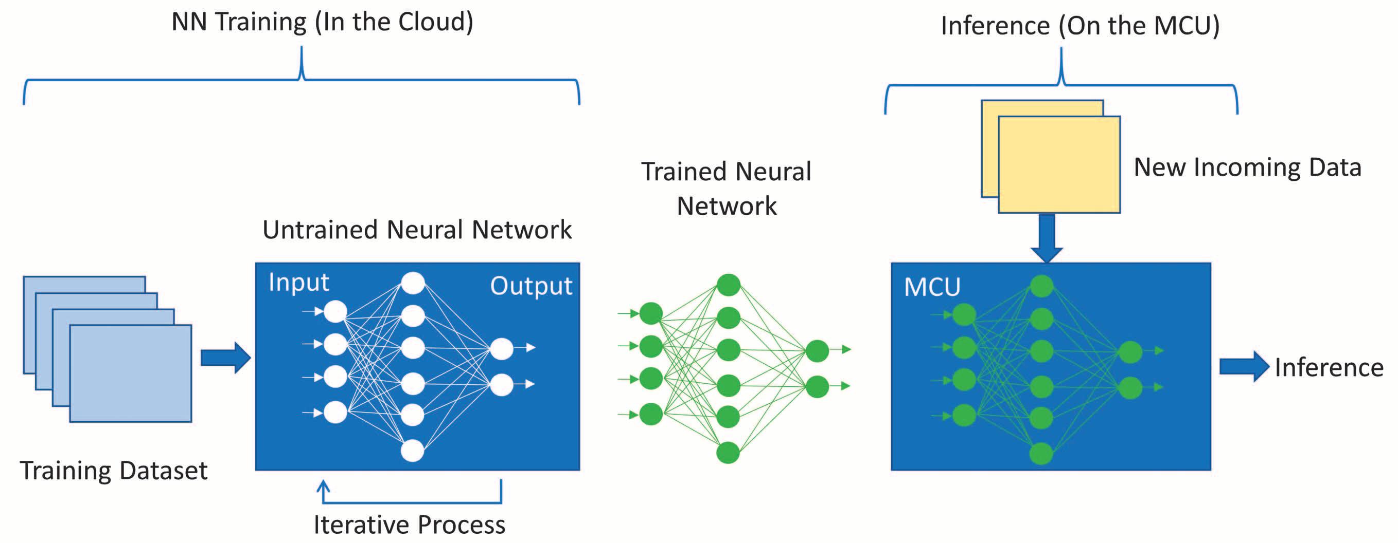
(NN) framework models like Caffe or Tensorflow Lite, suitable for MCU based end device solutions. The training of the NN model for machine learning is done in the cloud by AI specialists using tools provided by AI vendors. The optimization of the NN model and integration on the MCU is carried out using tools from the AI vendor and the MCU manufacturer. Inferencing is done on the MCU using the pre-trained NN model.
The first step in the process is done completely offline and involves capturing a large amount of data from the end device or application, which is then used to train the NN model. The topology of the model is defined by the AI developer to make best use of the available data and provide the output that is required for that application. Training of the NN model is done by passing the data sets iteratively through the model with the goal to continuously minimize the error at the output of the model. There are tools available with the NN framework that can aid in this process. In the second step, these pre-trained models, optimized for certain functions like keyword spotting or speech recognition, are converted into a format suitable for MCUs.
AIoT is enabled by higher compute capability of recent MCUs as well as availability of thin neural network (NN) frameworks that are more suited for resource constrained MCUs being used in these end devices. A neural network is a collection of nodes, arranged in layers that receive inputs from a previous layer and generate an output that is computed from a weighted and biased sum of the inputs.
The weights of this pre-trained NN model are fixed and can be placed in flash, thus reducing the amount of SRAM required and making this suitable for more resource constrained MCUs.
Implementation on MCUs
The AIoT implementation on MCUs involves a few steps. The most common approach is to use one of the available Neural Network
The first step in this process is to convert it into a flat buffer file using the AI converter tool. This can optionally be run through the quantizer, in order to reduce the size and optimize it for the MCU. This flat buffer file is then converted to C code and transferred to the target MCU as a runtime executable file. This MCU, equipped with the pre-trained embedded AI model, can now be deployed in the end device.
When new data comes in, it is run through the model and an inference is generated based on the training. When new data classes come in, the NN model can be sent back to the cloud for re-training and the new re-trained model can be programmed on the MCU, potentially via OTA firmware upgrades. There are two different ways that an MCU based AI solution can be architected. For the purpose of this discussion, we are assuming the use of Arm Cortex-M cores in the target MCUs.
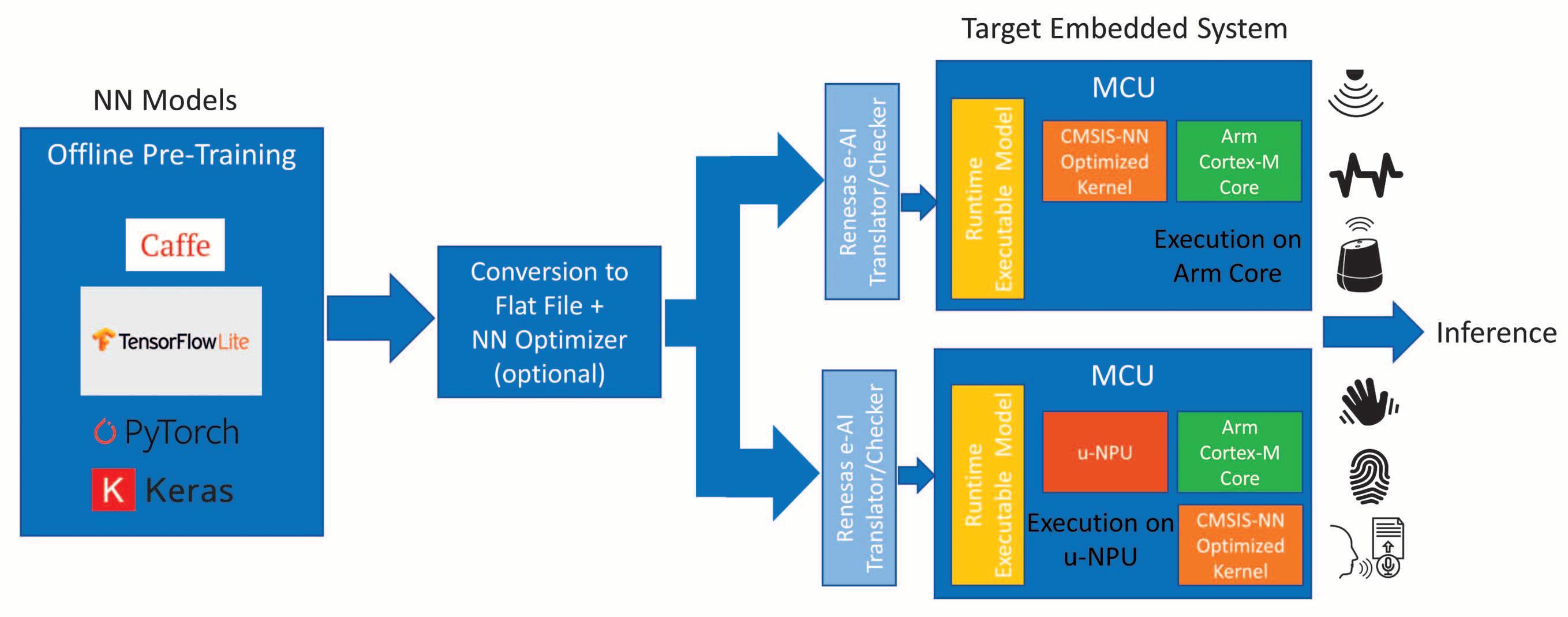
In the first method, the converted NN model is executed on the Cortex-M CPU core and is accelerated using the CMSIS-NN libraries. This is a simple configuration that can be handled without any additional hardware acceleration and is suited for the simpler AI applications such as keyword spotting, vibration analysis and sensor hubs.
As MCUs push the performance boundaries to higher levels, closer to that expected from MPUs, we expect to start seeing full AI capabilities including lightweight learning algorithms and inference, being built directly on MCUs.
Renesas and AI

Renesas has a comprehensive family of Arm based MCUs, the RA family, that are capable of running AI applications. All RA family MCUs support Arm Cortex-M cores and a rich feature set that includes on-chip Flash and SRAM and serial communication peripherals, Ethernet, graphics/HMI and analog features. They also support advanced security with symmetric and asymmetric cryptography, immutable storage, isolation of security assets and tamper resistance.
form (C/C++ based) that is usable by the MCU and assist in embedding the pretrained NN model on the target MCU. This AI enabled MCU can now be deployed in IoT end devices.
Implementation of AI on resource constrained MCUs will increase exponentially in the future and we will continue to see new applications and use cases emerge as MCUs push the boundary on performance and blur the line between MCUs and MPUs, and more and more “thin” NN models, suitable for resource constrained devices, become available. In the future, with an increase in MCU performance, we will likely see implementation of lightweight learning algorithms in addition to inference, being run directly on the MCU.
A more sophisticated and higher performance option involves including an NN accelerator or Micro Neural Processing Unit (u-NPU) hardware on the MCU. These u-NPUs accelerate machine learning in resource constrained IoT end devices and might support compression that can reduce power and size of the model. They support operators that can fully execute most of the common NN networks for audio processing, speech recognition, image classification, and object detection.
The networks that are not supported by the u-NPU can fall back to the main CPU core and are accelerated by the CMSIS-NN libraries. In this method, the NN model is executed on the uNPU. These methods show just a couple of ways to incorporate AI in MCU based devices.
Renesas is working closely with ecosystem partners to bring end-to-end AI solutions in predictive analytics, vision and voice applications, amongst others. These new AIoT technologies have opened up significant new opportunities for Renesas MCUs. Applications using these capabilities span market segments such as industrial automation, smart homes, building automation, healthcare and agriculture. Renesas’s “e-AI” (embedded AI) solution uses both popular NN models, Caffe developed by UC Berkeley and TensorFlow from Google. It utilizes Deep Neural Network (DNN), a multilayered network, that is particularly suited for applications involving image classification, voice recognition or natural language processing. The Renesas e-AI tools embedded in the e2 Studio Integrated Development Environment convert the NN model into a
This will open up new markets and applications for MCU manufacturers and will become an area of significant investment for them.
Kavita Char is a Senior Staff Product Marketing Manager at Renesas Electronics America. She has over 20 years of experience in software/applications engineering and product management roles. With extensive experience in IoT applications, MCUs and wireless connectivity, she is now responsible for definition and concept to launch management of next-generation Arm based high performance MCUs and solutions at Renesas.
Renesas Electronics Corporation introduced the R9A06G061 power line communication (PLC) modem IC. The R9A06G061 delivers high-speed communication at up to 1 Mbps over long distances of a kilometer or more, without the need for relays, expanding the range of practical applications for PLC. Optimized analog peripheral functions reduce the number of external components required, allowing for less expensive and more compact systems. With this combination, the new R9A06G061 is ideally suited for heating, ventilation, and air conditioning (HVAC) control, lighting system control in office buildings, and string monitoring and power conditioner control in solar power systems. Since it does not require the installation of dedicated cables, the R9A06G061 can enable low-cost system monitoring in applications such as monitoring of cellular antennas or motors in submersible pumps.
While Renesas’ current R9A06G037 PLC modem IC supports the G3-PLC, PRIME and Meters and More standards and can be used to implement large-scale multihop networks with a mesh topology, the new R9A06G061 is designed specifically for configuring simple peer-to-peer (P2P)
networks with a bus or star topology. Improved transmission drive capability enables designers to increase the number of devices that can be connected twofold to more than 200 without the use of additional line drivers. In addition, the IC’s superior noise tolerance makes it suitable for a wide range of applications and environments.
“The cost and extended construction time associated with the installation of dedicated signal lines as well as the maintenance cost of additional devices are key issues for building and infrastructure device management,” said Toshihide Tsuboi, Vice President, Industrial Automation Business Division at Renesas. “PLC is an outstanding solution that overcomes these issues, and I am confident that our new product, designed specifically for P2P networks, will further broaden the scope of practical applications for PLC.”
Renesas also released evaluation kits for AC and DC power lines, respectively. These evaluation kits, along with tools for evaluating communication performance that run on a PC, support communication characteristics evaluation, error analysis, and troubleshooting. Renesas provides
both the evaluation software and a variety of documentation to enable developers to immediately begin development and debugging. Design data for the hardware of the evaluation kits is available upon request in order to support more rapid product development.
Renesas has combined the R9A06G061 with complementary analog and power offerings that work together seamlessly to create Winning Combinations for a variety of applications. An example of one of these Winning Combinations includes Hi-Speed and Long-Distance Power Line Communication Unit for AC line / DC Line that also combines AC/DC and DC/DC converters. Renesas offers more than 250 Winning Combinations with compatible devices for a wide range of applications and end products. They can be found at renesas.com/win.
The R9A06G061 ICs and evaluation kits are available now. More details can be found at https://www.renesas.com/R9A06G061
Renesas Electronics Corporation
https://www.renesas.com

Secure Thingz, an IAR Systems® Group company delivering advanced development and provisioning platforms to secure the IoT, today announced their partnership with Intrinsic ID, the leading provider of Physical Unclonable Function (PUF) security IP. By working together, the companies intend to provide strong integration of Intrinsic ID’s physical unclonable functions (PUF) within Secure Thingz development and provisioning solutions.

Establishing a supply chain of trust has never been more important as products and devices share sensitive information and provide vital services. With this partnership, companies will be able to develop products with unique identities and integrated confidentiality. This can then be carried through the entire development, manufacturing, and lifetime of a product through a secure microcontroller execution environment and an immutable boot path to a root of trust boot manager that verifies subsequent software before execution.
“Physical unclonable functions are vital components in many modern devices, with leading vendors integrating them into their microcontroller offerings for IoT security,” stated Haydn Povey, CEO, Secure Thingz. “Together with Intrinsic ID, we will enable this critical capability to be integrated into a wide array of embedded systems to deliver protection of provisioned data, together with the creation of root keys.”
“We believe PUF technology is fundamental for the security of embedded applications in the IoT environment,” said Pim Tuyls, CEO, Intrinsic ID. “Secure Thingz is a key player in delivering solutions to secure the IoT and this partnership will enable and support an accelerated adoption of PUF technology, providing a key differentiator for delivering chain-of-trust implementation across the embedded marketplace.”
By using Secure Thingz’ security solutions, companies can implement a robust root of trust as part of the development process and extended into programming and provisioning, supporting the use of PUF technology in volume programming and provisioning services across the world. More information is available at www.securethingz.com.
►IAR Systems | https://www.iar.com
Developing and testing embedded systems means working with a live target system which is under the power. For embedded designs which feature high-voltage circuits like Automotive battery management systems, iSYSTEM offers a series of Galvanic Isolation Adapters which prevent developers from personal injury and equipment from electrical damage without affecting signal integrity.
Preventing personal injury and electrical damage to both development equipment and target
iSYSTEM Galvanic Isolation Adapters protect developers and development equipment.
Galvanic isolation is required where two or more electric circuits communicate with each other, but their grounds may be at different potentials. It is an effective method of breaking ground loops between the different circuits, preventing unwanted current from flowing between the two units sharing a ground conductor. Galvanic isolation is also important for safety reasons, preventing accidental current from reaching ground through a person’s body.
iC5700 BlueBox debugger and the target microcontroller. The BlueBox and the embedded target are separately powered and isolated from each other. The Galvanic isolation adapters are powered separately as well via a USB-C Power supply adapter. A grounding wire connected to the BlueBox and the embedded target circuit wires out the ground potential – which can exceed well over 1000V even before any of the devices are powered up – between the two components and prevent their destruction.
The iSYSTEM Galvanic Isolation Adapters are being interposed as electrical isolation between development equipment like a development PC on one side and on the other side e.g., the
Typical setup: The iSYSTEM Galvanic Isolation Adapter is interconnected between development PC and debugger (here an iC5700 BlueBox) and target MCU.
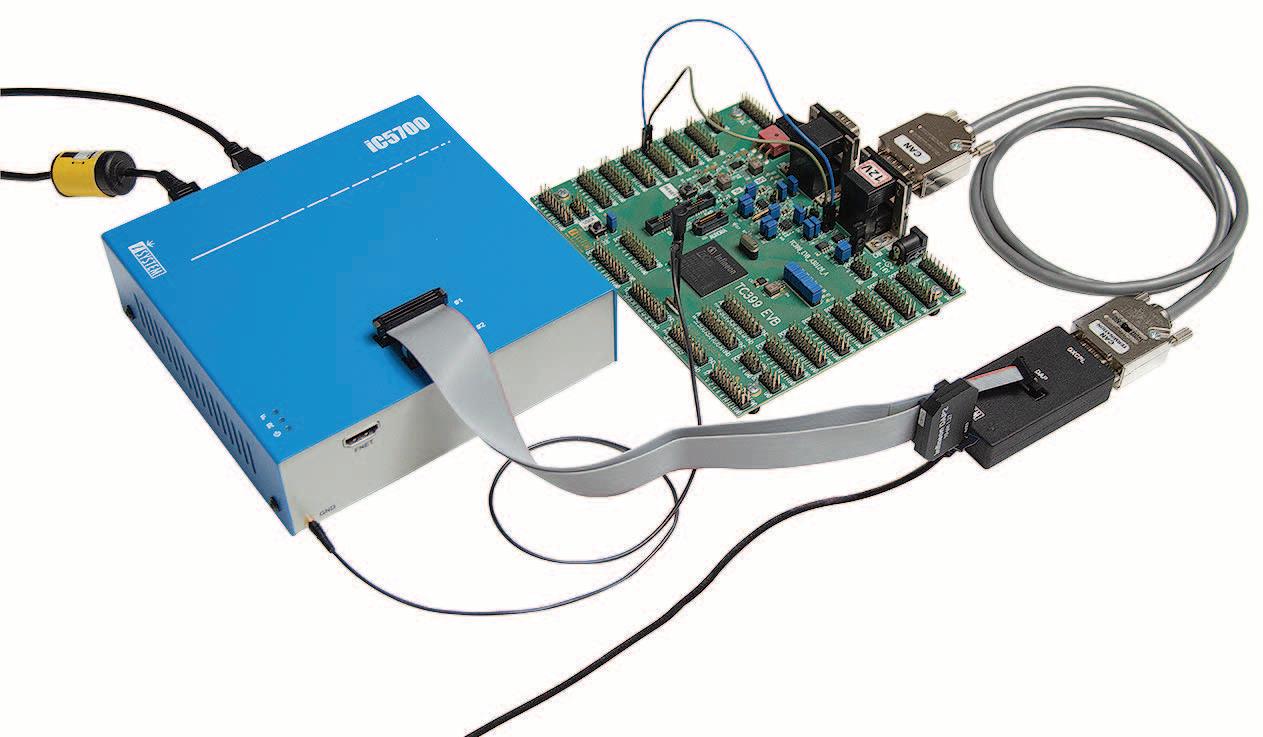
The adapters provide a basic isolation that withstands high voltages. However, when dealing with potentially hazardous voltages it is mandatory to have a second protection measure in place, in case the first insulation barrier fails.
The iSYSTEM Galvanic Isolation Adapters are available for Infineon AURIX, Arm Cortex and NXP / STMicroelectronics Power Architecture MCUs.
Further Links and Resources
iSYSTEM Galvanic Isolation Adapters: https://www.isystem.com/products/hardware/galvanic-isolation-adapters.html
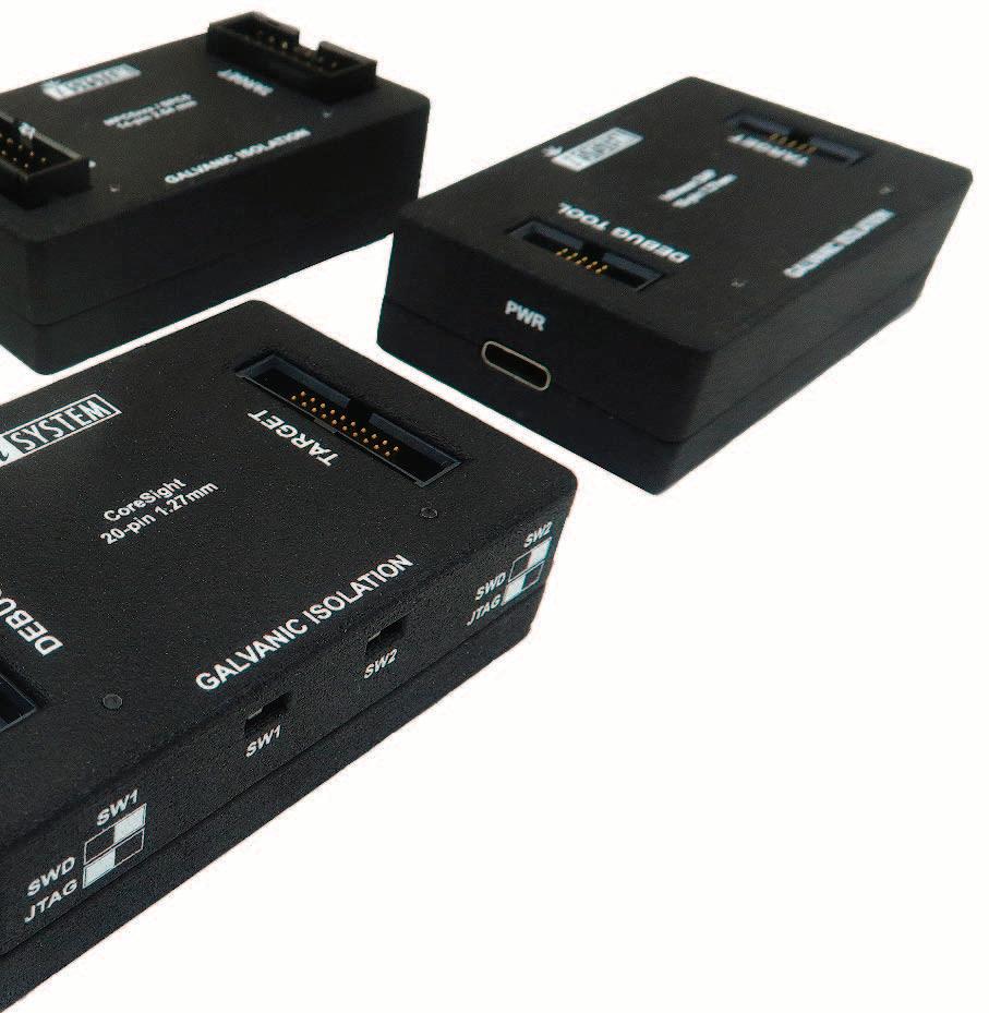
Technical Notes: https://www.isystem.com/files/content/downloads/documents/technical-notes/iSYSTEM_TN_Galvanic_Isolation.pdf
►iSYSTEM https://www.isystem.com

802.11ax, also known as WiFi 6, succeeds 802.11ac (WiFi 5) and thus now presents the 6th generation of the WiFi standard, which was first publicly established on the market in its birth year of 1999 with version 802.11b. With the new generation, the standard has also been consistently further developed and continues to build on the advantages of WiFi 5 in terms of efficiency, flexibility and scalability. WiFi 6 also offers higher speeds and capacities compared to WiFi 5 and thus forms the foundation for future-oriented networks.
In the course of this, 8DEVICES has developed two new module solutions, both based on the latest WiFi 6 chip generation from Qualcomm. Mango follows the approach of a SOM (System on Module), where the application can be completely
integrated on the module. Pineapple, on the other hand, follows the radio module approach, i.e. it only offers the radio technology, a host processor, memory and peripherals/interfaces are required to run an application.
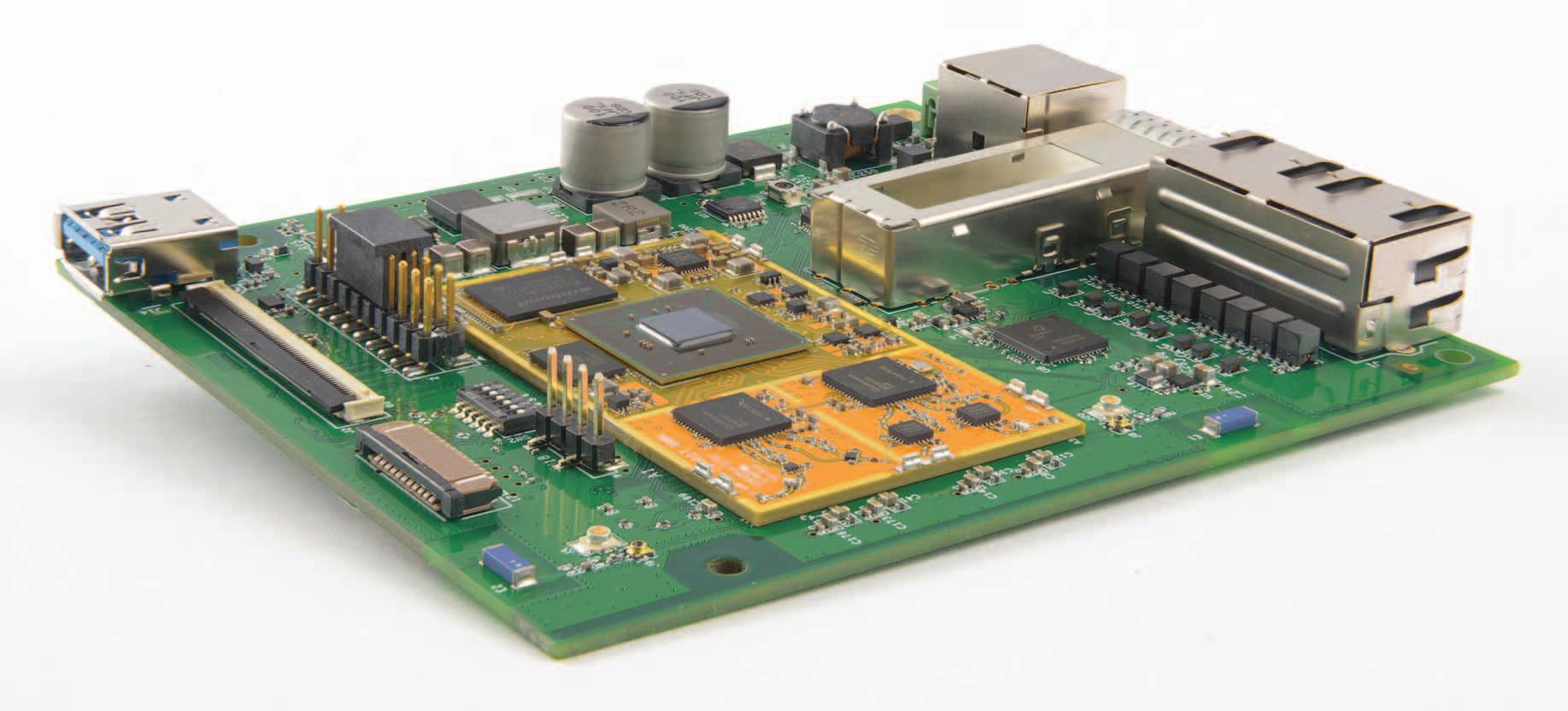
Admittedly, the names Mango and Pineapple do sound a bit exotic and are more reminiscent of a beach vacation in the Caribbean than of 6th generation WiFi solutions. However, if you look through the IEEE standardization documents of WiFi6 and internalize the underlying complexity and performance, the term exotic no longer seems too far-fetched for module solutions that master this technology 100%. So let's be surprised.
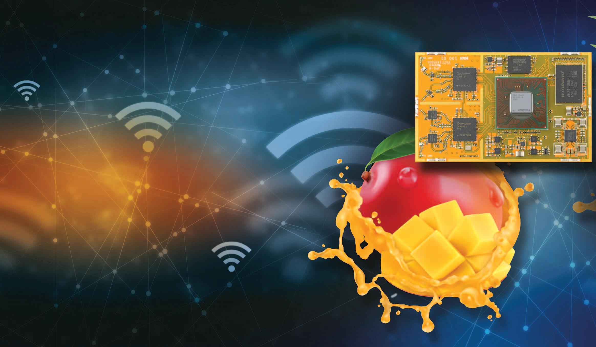
The SOM approach called Mango is based on Qualcomm's new SoC family IPQ60xx. The user has access to 4 x Cortex-A53 clocked with 1.2 GHz or 1.8 GHz.
Furthermore, 512 MB DDR @ 933 MHz and 32 MB NOR Flash are available.
In contrast to other SOM solutions, where the NAND flash memory is directly integrated on the module, Mango requires the connection of an external NAND memory device. However, this also results in a small advantage, because the user can dimension the memory size for his application himself and is not confronted with any memory restrictions.
2 x PSGMII, QSGMII and SGMII+ interfaces are available for the connection of Gb Ethernet. On the other hand, the interfaces 64xGPIO, 1xPCIe 3.0 (Mango-I only), 1xUSB3.0, 1xUSB2.0, 2xUART, 3xSPI, 2xI2C, 4xPWM, 1xJTAG, 1xI2S/TDM and 1xSDIO3.0/eMMC are fully integrated and don’t need any external driver devices to run these interfaces.
In terms of WiFi, Mango supports 802.11 b/g/n/a/ac standards in addition to 11ax and offers multi-user MIMO 2x2 mode with DBS (Dual Band Simultaneous).
Mango is available in two versions:
Mango: CPU clock @1,2GHz, without PCIe, temperature grade: 0°C ... +65°C.
Mango-I: CPU clock @1,8GHz, with PCIe, temperature grade: -40°C ... +85°C.
Samples and DVKs are available in our sample shop:
https://www.codico.com/en/mango https://www.codico.com/en/mango-iindustrial-temperature-grade https://www.codico.com/en/mango-dvk

Pineapple is based on Qualcomm's brand new QCN-9074 radio IC, which supports 3 bands 2.4GHz, 5GHz and 6GHz (WiFi6E) in
All 3 variants have in common that each is offered in 4 different package designs. The LGA package, with a small form factor of 35x47mm, offers space-saving integration on a carrier PCB, where the antennas can be connected to the 4 antenna pads of the module in the form of U.FL connectors or in a PCB antenna design.
In addition, 3 other versions are offered as plug-in cards in a 50x61mm form factor with a mini-PCIe, M.2 A+E or M.2 B+M interface, where 4 x U.FL connectors are already integrated on the cards.
This results in 3 × 4 = 12 different module designs. If it is taken into account here that in the course of the year each version will also be available in the industrial temperature grade -40°C to 85°C (the current solutions offer 0°C to 65°C), this results in a total of 24 different module variants.
Also encouraging is the news that all modules will be supported by the Linux mainline driver from version 4.4.60 upwards. Of course like Mango, all modules will be certified according to RED, FCC and IC in the course of the year.
Samples for Pineapple 5 and 6 can be ordered in our Sample Shop:
https://www.codico.com/de/pineapple5
https://www.codico.com/de/pineapple6
More information about Mango and Pineapple is provided on our official support page:
http://downloads.codico.com/misc/AEH /8DEVICES
a 4x4 MIMO antenna configuration via a PCIe interface. Accordingly, 8DEVICES offers 3 variants with the following product names corresponding to the bands:
Pineapple 2: 2400-2500MHz
Pineapple 5: 4920-5925MHz
Pineapple 6: 5925-7125MHz
Pineapple 5 and 6 support up to 27 dBm per antenna @ HT20/40/80/160, while Pineapple2 supports up to 28 dBm per antenna, but is limited to HT20/40.
Pineapple 5 and 6 achieve a maximum data rate of 4804 Mbps in an HT160 and MIMO 4x4 configuration. Pineapple2 is still at a maximum of 1147 Mbps with HT40 and MIMO 4x4.
►CODICO
https://www.codico.com
Contact for Romania: Gergely Balogh
Tel: +36 30 867 0687
e-mail: gergely.balogh@codico.com
Renesas Electronics Corporation introduced the RAA227063 Smart Gate Driver for brushless DC (BLDC) motor applications. The new device is programmable via an SPI interface, enabling it to support both motors with rotor position sensors and sensorless applications. It also provides programmable gate drive voltage, offering support for N-channel MOSFETs typically used in motor inverter designs, as well as GaN FETs used where high power density is required. The RAA227063 is scalable to support multiple MCUs, including a wide range of Renesas offerings.
In addition to its unique flexibility, the RAA227063 three-phase FET driver is highly integrated. It includes a 500 mA buck-boost converter that powers lowvoltage logic directly from the battery pack with better power efficiency (90%) compared to traditional LDOs (40%). It also includes a 200 mA LDO regulator that can power both an MCU and additional analog peripherals.
Three integrated current sense amplifiers with programmable gain enable easy programming for multiple shunt configurations. This high level of integration simplifies design, cuts overall BOM cost, and reduces board space requirements by 30 percent or more.
“Motor control customers around the world have asked us for flexible solutions that enable fast design cycles and high integration to reduce cost and space,” said Davin Lee, Vice President of the Industrial Analog Division in Renesas’ IoT and Infrastructure Business Unit. “The RAA227063 delivers all of these features and complements our industry-leading MCU portfolio.”
Smart Gate Driver
• High integration simplifies inverter design, allows the ability to scale MCUs
• Programmable gate drive voltage drives both N-MOSFETS and GaN FETs
• Supports trapezoidal, 150° drive and vector motor control algorithms
• Back electromotive force (BEMF) sensing simplifies sensor-less control
• Programmable via SPI to support BLDC motors with rotor position sensors such as hall sensors or encoders
• Programmable up to three-phase current sensing
• Scalable to support multiple MCUs
• Extensive fault protection functions protect inverter from catastrophic failure and provides fault warnings for easy troubleshooting
• Adaptive dead time minimizes switching power losses
• Sample and hold allows use of general purpose MCUs with at least three ADCs and three timers to drive BLDC motors
Renesas has combined the RAA227063 with complementary components that work together seamlessly to create Winning Combinations for motor control solutions. An example of one of these Winning Combinations is the BLDC Traction Motor Drive design that also includes Renesas’ new RA6T2 MCU optimized for motor control applications.
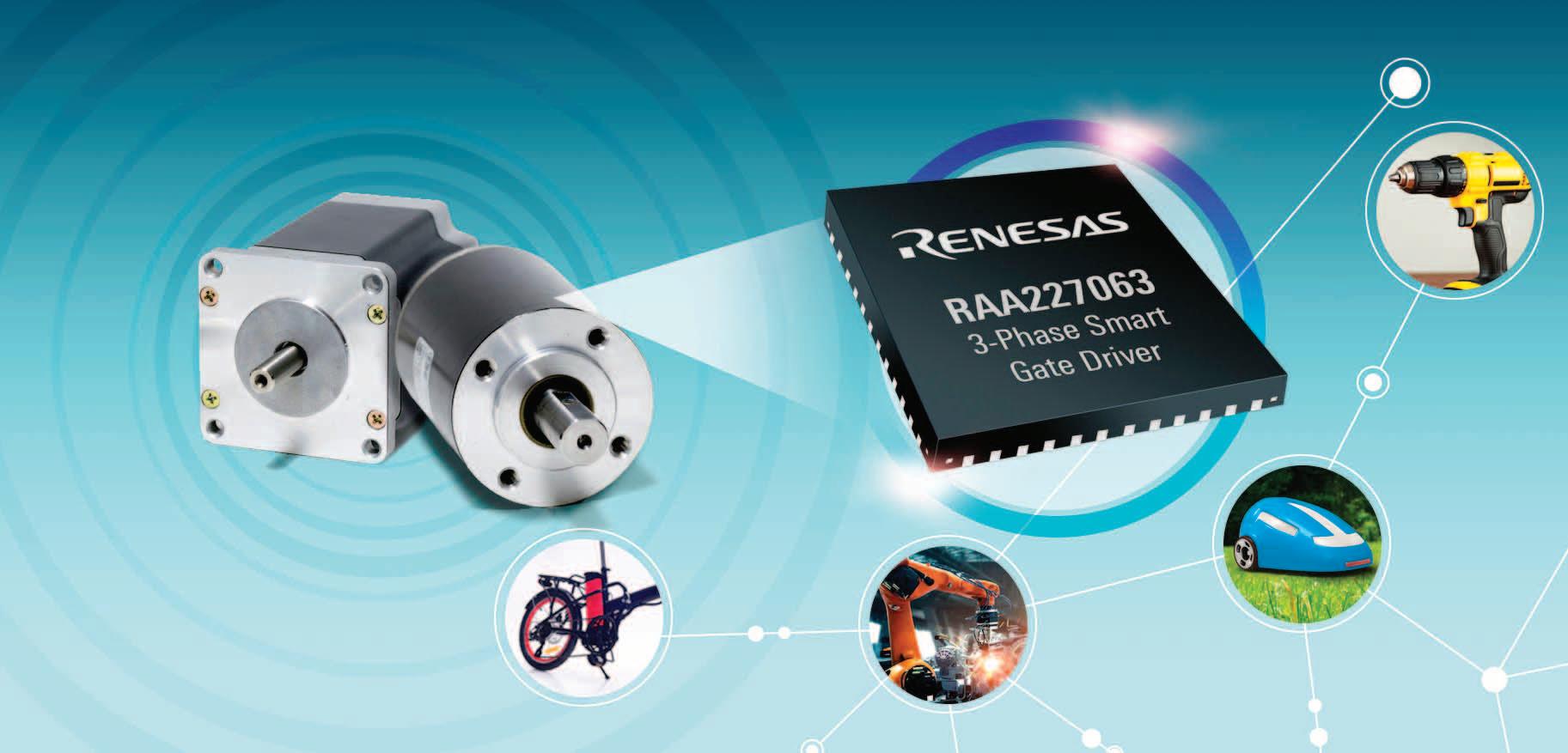
Renesas offers more than 250 Winning Combinations with compatible devices for a wide range of applications and end products. They can be found at https://www.renesas.com/win.
The RAA227063 is available today in a 7mm × 7mm 48-pin QFN package. Renesas is also offering the RTKA227063 evaluation kit that includes a 500W inverter that can use multiple CPU cards.
More details can be found at https://www.renesas.com/RAA227063.
Renesas Electronics Corporation
https://www.renesas.com


To meet multiple requests from registered exhibitors and enable all participants to plan with the maximum possible confidence, the embedded world Exhibition&Conference 2022 has been rescheduled: In close consultation with exhibitors the decision has been taken to postpone the exhibition and accompanying conferences until 21-23 June 2022. Exhibitions and congresses have been held again at the Exhibition Centre Nuremberg since September 2021 subject to a robust hygiene concept, and exhibitors and visitors have responded extremely positively and with a sense of responsibility. At the same time, NürnbergMesse is paying attention to the individual needs of its customers and participating sectors. This has led to different decisions for different events. Current developments in the Covid-19 pandemic are causing uncertainty for many exhibitors at embedded world, for example. Benedikt Weyerer, Executive Director embedded world, comments: “By deciding at an early stage to defer embedded world 2022 until summer, we are meeting the wishes of many exhibitors and enabling them to plan with confidence. We are very grateful for the many constructive conversations with industry representatives, which provided significant encouragement for this decision. Together with the exhibitors, we are looking forward to seeing the international embedded community again in Nuremberg from 21 to 23 June next year!”
The embedded world Conference will be held in parallel with the exhibition. As usual, this highly regarded conference will focus on the latest topics of interest, and participants can look forward to seeing mega-trends on the agenda. Professor Axel Sikora, Chairman of the embedded world Conference, is looking forward to the 20th event in the series: “The embedded world Conference 2022 will once again highlight the current state of research and development. This will be another opportunity for us to combine wide-ranging themes relating to the development of complex, comprehensive systems with special themes of current interest such as RISC ‑V and solutions to problems in times when supplies of chips are tight, and also long-term mega-trends such as artificial intelligence (AI), open source solutions and secure connectivity. The embedded world Conference brings together the leading thinkers in this area, who are already developing innovations for the future.”
►NürnbergMesse | https://www.embedded-world.de/en
Digi-Key Electronics, which offers the world’s largest selection of electronic components in stock for immediate shipment, has partnered with Seeed Studio and Machinechat to launch the industry’s first private LoRaWAN-in-a-Box solutions for the Internet of Things (IoT).
“Digi-Key is proud to be the exclusive global source for these turnkey, industry-first LoRaWAN solutions,” said Robbie Paul, director of IoT business solutions at Digi-Key. “Wireless connectivity technologies like LoRaWAN are leading the way for mass adoption of IoT, and we are excited to inspire developers and systems integrators around the world with many new possibilities available to them with these solutions.”
The ready-to-use solutions combine Seeed Studio’s industrialgrade LoRaWAN (Long Range Wide Area Network) IoT sensors and gateways with Machinechat® JEDI Pro Seeed Studio Edition software, allowing for rapid IoT deployments and enhanced security features that give users complete control over device data, ultimately saving time and reducing technical complexity and costs. The first LoRaWAN-in-a-Box solution is focused on rapid deployment of smart agriculture and precision farming projects.
“For more than 13 years, Seeed Studio has been at the forefront of introducing innovative IoT enablement solutions,” said Eric Pan, CEO of Seeed Studio. “By bundling our award-winning SenseCAP LoRaWAN hardware solutions with Machinechat’s innovative and easy-to-use software, Digi-Key customers worldwide will be able to build and deploy robust, private LoRa IoT deployments in days versus weeks.”
“Machinechat is thrilled to be part of this partnership with Digi-Key Electronics, a worldwide leader in offering the best of breed and innovative technologies for IoT, and Seeed Studio, a global leader in IoT enablement hardware,” said Sanjeev Datla, CEO of Machinechat “Our combined private LoRaWAN-in-a-Box solutions enable systems integrators and enterprise IT teams to rapidly transform their ideas into transformational IoT digital projects.”
Seeed Studio SenseCAP LoRaWAN Solutions
Designed for commercial IoT applications, including smart agriculture, precision farming, and smart city use cases, SenseCAP’s industrial-grade LoRaWAN sensors, data logger, and gateway solutions are designed for rapid installation and deployment. Features include:
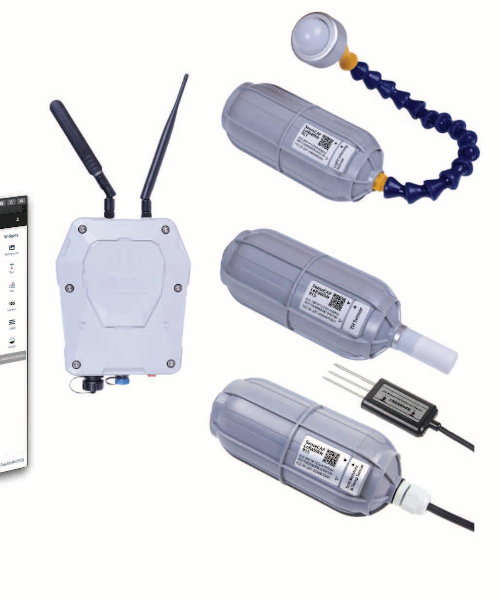
• Support for LoRaWAN protocol Class A
• Ultra-wide-distance transmission: up to 10km line of sight
• Support for multiple ISM bands: EU868, US915, AU915, AS923
• Support for Ethernet backhaul; cellular optional
• Industrial grade protection: IP66 enclosure, suitable for outdoor applications and able to operate in temperatures from -40°C to +70°C (up to 85°C for SenseCAP sensors)
• High reliability and stability
• Sensor battery life of 3+ years
Machinechat’s JEDI Pro Seeed Studio Edition is the industry’s most affordable IoT data monitoring and visualization software. Designed specifically for commercial IoT deployments, Machinechat JEDI Pro Seeed Studio Edition features include:
• Ingest data from Seeed Studio’s SenseCAP LoRa sensors using the integrated Seeed Studio data collector (Chirpstack installation required).
• Ingest data from virtually any device or sensor using integrated HTTP API server, TCP server and MQTT broker.
• Configure dashboards to visualize real time and historical data with line, area, tile, radial and data grid charts.
• Monitor data using integrated rules engine to trigger email notifications, SMS or execute external scripts (*email notification requires SMTP server. SMS requires Twilio account).
• Monitor whether devices and machines are online.
• Apply your custom business logic to IoT data through data collector and action plug-ins.
• Virtual data sensor allows developers and integrators to simulate project deployment scenarios
• Low code – focus on configuring, not coding.
• Single application binary that runs as a service with integrated database and managed local data storage.
• Modern browser-based user interface with SSL support and role-based user management
• Supports up to 200 devices/sensors.
• Available for Windows, macOS, Linux, Raspberry Pi and BeagleBone® platforms.
For more information about the LoRaWAN-in-a-Box solutions, visit here.
Headquartered in San Jose, California, Machinechat’s mission is to be the leading supplier of IoT data management solutions that dramatically reduce the cost and time spent developing and deploying IoT projects. Leveraging software-defined networking principles, Machinechat’s easy-to-use and affordable solutions enable IoT solution architects, developers and networking OEMs to quickly add data collection, processing of streaming data, data monitoring, and policy-based data management to their products and solutions. Machinechat is the developer of the JEDI One and JEDI Pro software solutions. Learn more at https://www.machinechat.io.
Seeed Studio, headquartered in Shenzhen, China, has been serving the global developer community since 2008, by providing open technology and agile manufacturing services, with the mission to make hardware more accessible and lower the threshold for hardware innovation. With Shenzhen’s vast resources and trusted technology and distribution partners around the world, Seeed strives to be the most integrated platform for creating hardware solutions for IoT, edge AI applications. By integrating the latest technology resources, Seeed offers the next generation hardware to help emerging applications scale.
►Digi-Key Electronics
https://www.digikey.com

The new “RDK2” development kit from Rutronik is a complete solution for firmware and hardware developers. Based on the “RDK2”, proof of concepts can be created quickly and the time-to-market of products is accelerated. The modular toolkit uses the PSoC62 microcontroller from Infineon Cypress and provides an excellent solution for applications in the Internet of Things, Industrial IoT (IoT, IIoT), Smart Wearables, and Smart Home.
With the new “RDK2” development kit, Rutronik is creating a unique offering to accelerate the pre-development and the market launch of products. The modular toolkit is particularly suitable for the development of proof of concepts. The areas of application are diverse. For example, the board can be used for applications in the areas Internet of Things, Industrial IoT (IoT, IIoT), Smart Wearables, and Smart Home. “The electronics industry thrives on innovation. That’s exactly what we demonstrate at Rutronik. The ‘RDK2’ has the advantage that the development of products is faster. It offers numerous useful features as well as interfaces and has exceptional flexibility also in terms of application options. All the components we use are available in Rutronik’s portfolio,” explains Stephan Menze, Head of Global Innovation Management
The board uses the PSoC62 from Infineon Cypress for this purpose. The microcontroller has a dual-core CPU and is ideal for secure edge computing and cloud applications.
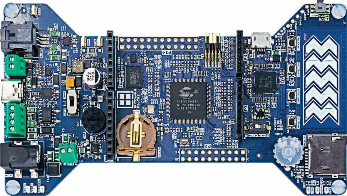
“Infineon welcomes the decision by Rutronik to implement the powerful PsoC62 microcontroller as the core of their newly developed board ‘RDK2’. With the PSoC 6 microcontroller family, Infineon offers a platform for IoT applications that enables connectivity, increased computing power, and security at low power consumption as well as cost. We continue to trust Rutronik’s service and customer reach and with the ‘RDK2’ they provide customers with a significant advantage in development,” says Susanne Horn, Vice President Distribution Management EMEA at Infineon.
The new and unique butterfly design allows improved handling. That ensures user-friendly access to the Arduino connectors and reduces possible interference from electromagnetic influences, especially with RF IoT Arduino Shields. For testing the analog-to-digital conversion, an integrated potentiometer is available. A special feature is that users have access to all pins of the PSoC62 via the Arduino headers. https://www.rutronik.com/development-stories/rutronikdevelopment-kit-rdk2/
►Rutronik | https://www.rutronik.com/
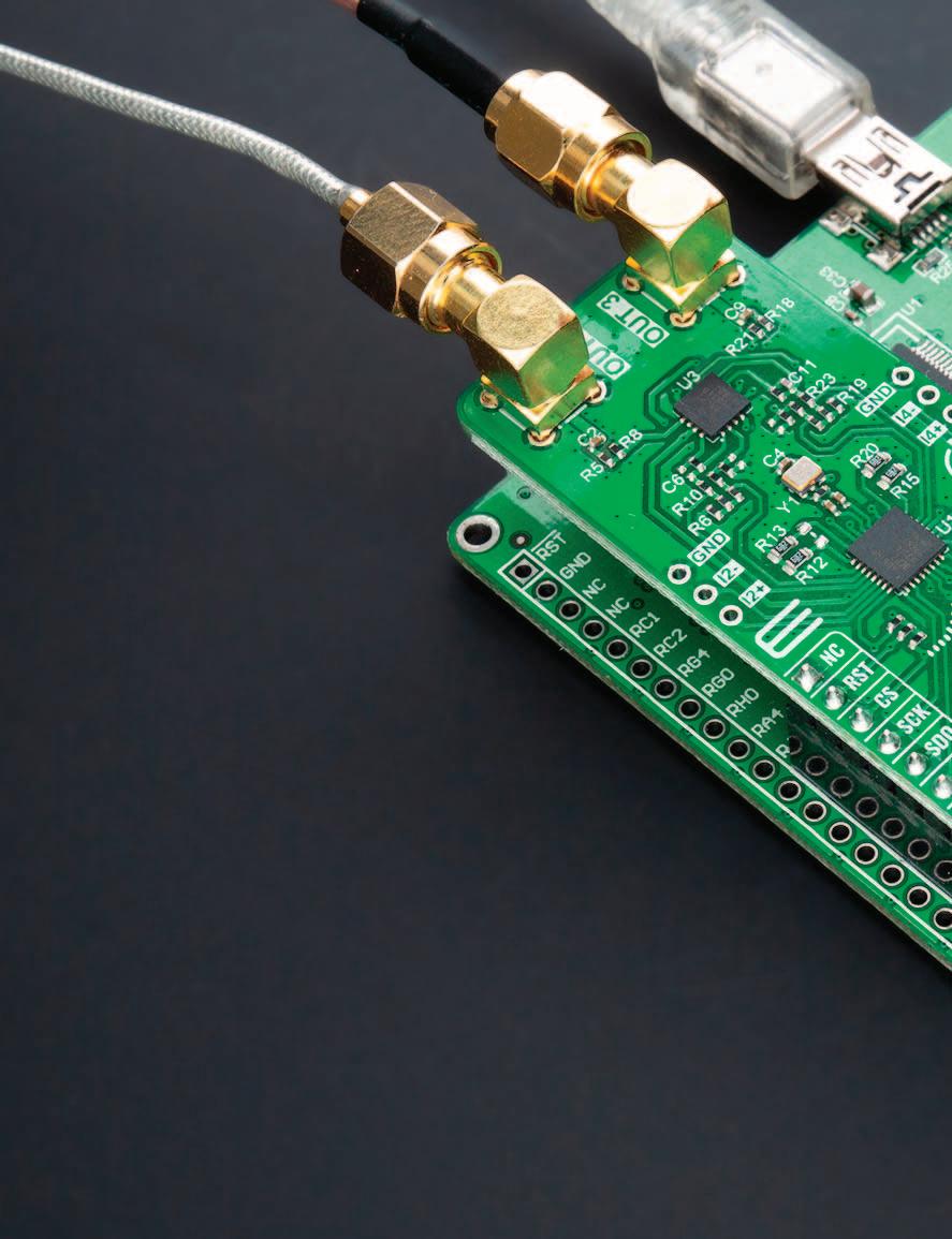
MikroElektronika (MIKROE), the embedded solutions company that dramatically cuts development time by providing innovative hardware and software products based on proven standards, has launched Waveform 4 Click – a member of its +1000-strong Click family of peripheral development boards – that operates as a signal generator for high-speed, highdynamic-range, multichannel complex waveforms required in applications such as ultrasound transducer excitation, medical instrumentation, portable instrumentation, signal generators, and arbitrary waveform generators.
Waveform 4 Click features Analog Devices’ AD9106, a quadchannel, 12-bit, 180MSPS waveform generator that integrates on-chip SRAM and direct digital synthesis (DDS) for complex waveform generation. The DDS facilitates a master clock sinewave generator at speeds of up to a 180 MHz with a 24-bit tuning word, allowing 10.8 Hz/LSB frequency resolution.
The AD9106 has a single frequency output and independent programmable phase shift outputs for each of the four integrated DACs. More, the integrated SRAM data can include directlygenerated stored waveforms, which can be accessed using the serial peripheral interface, amplitude modulation patterns applied to DDS outputs, or DDS frequency tuning words.
Click boards are based on the 16-pin mikroBUS™ standard for sockets on a development board invented by MIKROE ten years ago. Click boards enable design engineers to change peripherals easily, cutting months off development time. The company releases a new Click board nearly every day at 10am, and many leading microcontroller companies including Microchip, NXP, Infineon, Dialog, STM, Analog Devices Renesas and Toshiba now include the mikroBUS socket on their development boards.
Comments Nebojsa Matic, CEO at MIKROE: “Waveform 4 Click illustrates the huge range of functions that we have Clicks available for – at a low price. Don’t waste time reinventing the wheel – for just $109 designers can begin designing immediately.”
Waveform 4 Click is supported by a mikroSDK compliant library, which includes functions that simplify software development. This Click board™ comes as a fully tested product, ready to be used on a system equipped with the mikroBUS™ socket.
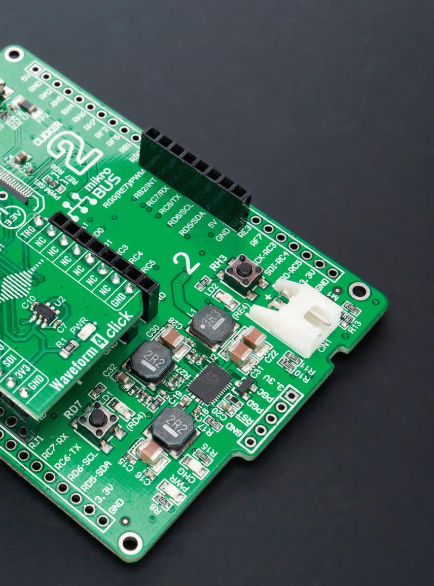
For more information about MIKROE’s full range of over 1000 Click peripheral boards, visit https://www.mikroe.com/click.
►MikroElektronika | https://www.mikroe.com
To provide additional learning opportunities for potential customers who are unable to attend trade fairs and exhibitions due to the pandemic, congatec has opened a digital trade show booth as a permanent exhibition on their website. A digital twin of the company’s engagement at real trade shows and events, the virtual trade show provides global access. The new congatec virtual exhibition complements a total of 11 in-person events worldwide by the end of 2021. Booth staff will be available round the clock on weekdays, allowing interested parties looking to get information and share ideas about the latest embedded and edge computing technologies to engage in conversation at any time.
“We invite the embedded community to check out our latest developments, free of any obligations. Visitors can interact with a member of staff via the chat functions. It’s the same low-threshold access to information we provide at live in-person trade shows.,” explains Christian Eder, Director Marketing at congatec
Visitors can view the latest presentations or chat with booth staff just like at a real trade show using any simple browser. It feels a bit like arriving before the trade show doors have opened, visitors can explore at their leisure with no pressure. Getting the information at the virtual booth is only marginally different from what you’d expect from a visit to an in-person event.
The virtual booth is designed as a central information hub for congatec’s latest technologies, products and service offerings. It includes current product demonstrations and application examples as well as presentations on the latest technologies. A sales partner area and a library to browse through complete the offering. Potential job applicants will also find a list of vacancies and journalists an overview of the latest news. If a press conference is planned, this will be indicated separately as usual and individual invitations sent out. Follow the link to visit the virtual booth: https://www.congatec.com/fileadmin/virtual-fair-v2/ ►congatec | https://www.congatec.com
Waveform 4 peripheral development board based on ADI's AD9106, quad-channel, 12-bit, 180MSPS waveform generator
This article briefly explores general AC/DC power supply application considerations. It then gives examples of three boardmounted AC/DC power conversion options from RECOM Power’s RACxx-K Series, identifying key features and benefits of specific products and how they are applied.
Author: Rolf Horn, Applications Engineer at Digi-Key Electronics

Board mounted AC/DC power supplies from 3 to 20 watts are being used across a growing variety of applications including Internet of Things (IoT) and Industrial IoT (IIoT), Industry 4.0, industrial automation, audio visual equipment, information technology equipment (ITE), smart house/ building, white goods, and consumer appliances. While it can be tempting to try and design low-wattage AC/DC power supplies, the process is more complex and time-consuming than it may appear to be at first glance. Designs need to meet challenging performance requirements including wide input voltage ranges, peak power delivery, and high-power densities. They also must be certified to numerous international standards for safety, efficiency, standby power, and electromagnetic compatibility (EMC).
Instead, designers can use compact boardmounted AC/DC power supplies that are certified to all relevant international performance standards, speeding time to market. These efficient power supplies have wide input voltage ranges and can accept AC or DC inputs for flexibility and worldwide compatibility.
AC/DC power supplies can be connected in series or parallel to provide higher power levels or redundant hot-swap operation (Figure 1).
Parallel connected power supplies (the lower configuration in Figure 1) can be used to provide higher currents or higher reliability through redundancy. Higher currents are possible when both power supplies are operated at or near their fully rated output currents. The output voltage does not change, but the available current is increased, upping the output power. Redundant power configurations use multiple power supplies to increase system reliability, not to increase the available power level. Redundant configurations can take several forms. In one topology, the system is configured to draw power from only the “primary" power supply during normal operation and to automatically switch to the “backup” power supply in the event that the primary supply fails.
N+1 redundancy is another common topology used to increase power supply reliability. An N+1 system consists of two or more power supplies.
In Figure 1, the lower configuration can be used as a redundant architecture with “N” = 1. In this case, each of the power supplies runs at 50% of capacity during normal operation, and each one can provide the full load power should the other power supply fail. Instead of paralleling power supplies to increase the available power, it can also be increased by connecting power supplies in series (top configuration in Figure 1). In this example, both power supplies have the same output voltage, VO, and the series configuration delivers 2V O Since the current delivered to the load does not change, doubling the voltage doubles the effective power.
Two AC/DC converters can be connected in series for higher voltage (top) or in parallel for higher current and/or redundant operation (bottom) © RECOM Power
Both of the configurations in Figure 1 include ORing diodes to isolate the outputs of the power supplies. If one of the power supplies fails, the ORing diodes protect the system from catastrophic failure.
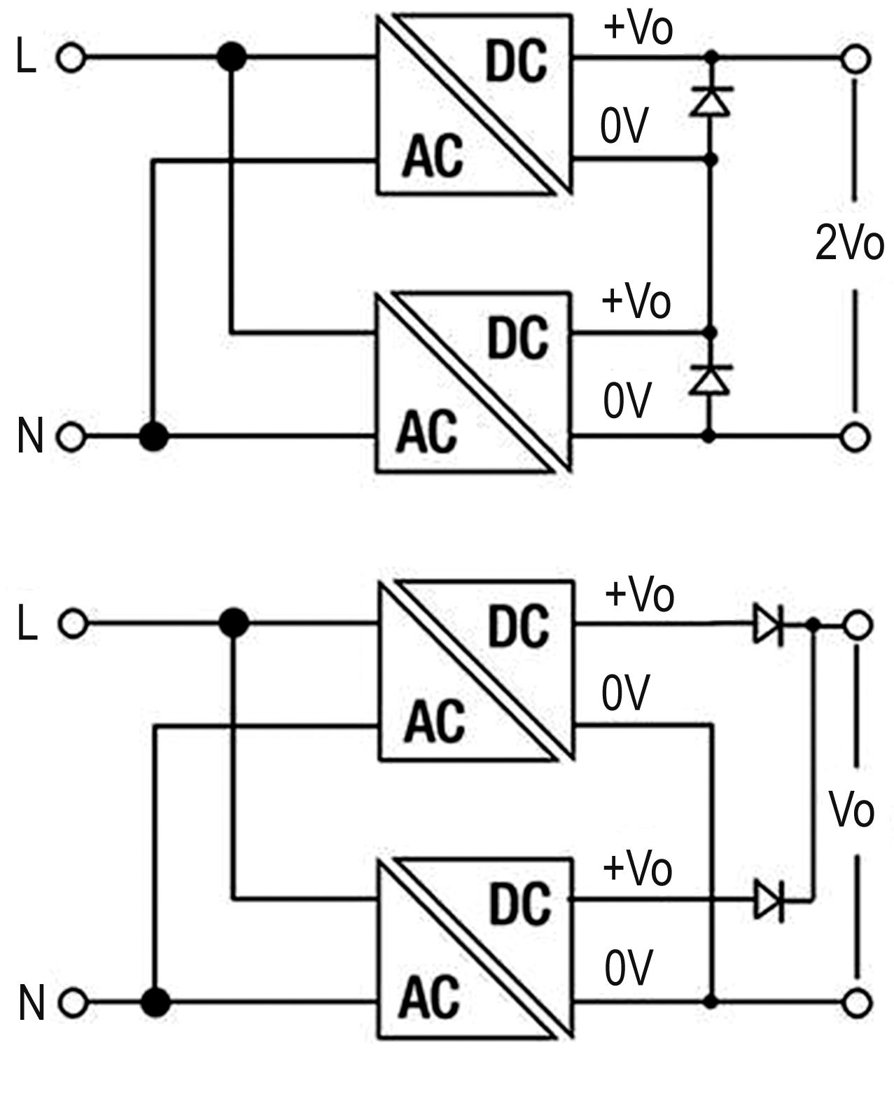
The ORing diode current rating should be greater than the output current rating of the power supply, and the breakdown voltage rating must be greater than the power supply output voltage.
While there are several ways to connect the outputs of two or more AC/DC power supplies together for additional functionality, it is not possible to connect the inputs of two AC/DC converters to increase the input voltage range. It’s for that reason that wide input (also called universal input) AC/DC power supplies are increasingly popular. Fuse protection is also an important consideration for AC/DC power supply inputs (Figure 2).
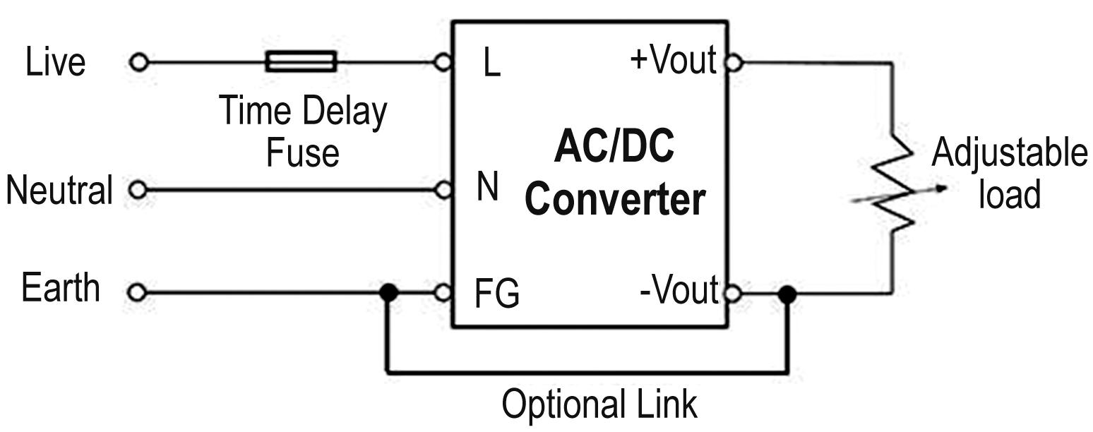
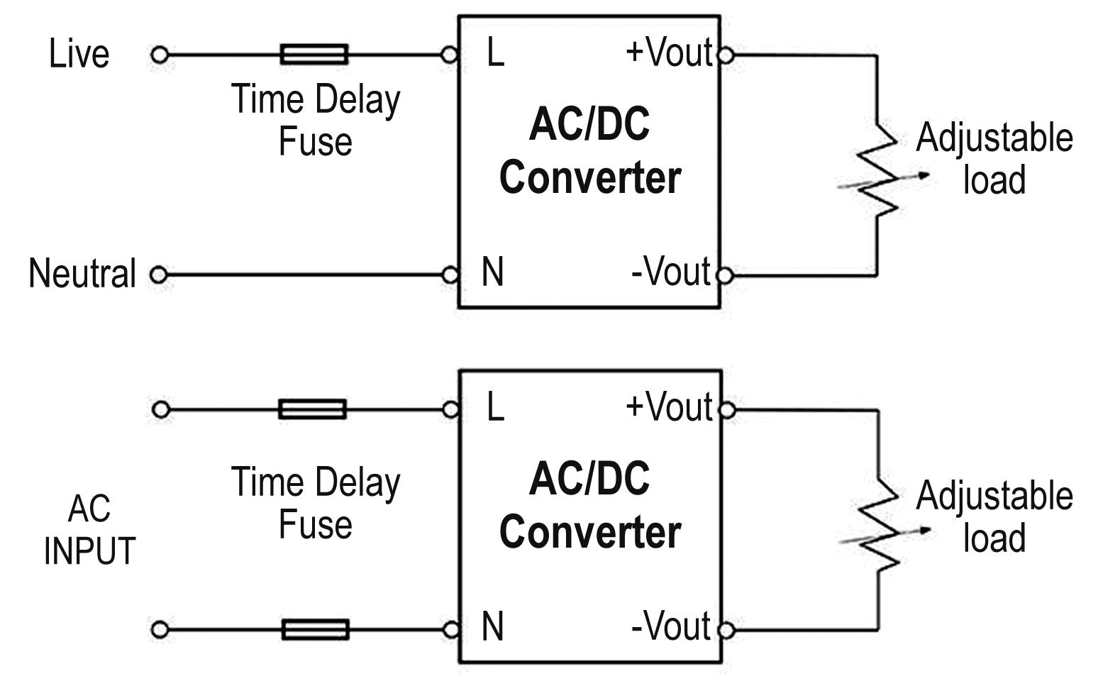
The use of time delay (also called slow blow) fuses is generally recommended.
For designers of IoT, IIoT, and household applications requiring 3 watts of power, RECOM offers the RAC03E-K/277 AC/DC power supply which delivers a single, tightly regulated 12 volt DC output (other models are available with outputs from 3.3 to 24 volts DC).
These internationally certified power supplies feature an enhanced wide input voltage range from 85 to 305 volts AC or 120 to 430 volts DC and conform to ErP standby power requirements. The RAC03E-K/277 series has a wide operating temperature range, delivering full output power from -30 to +75°C (except for 3.3-volt output units which deliver full power to +70°C) under natural convection cooling (Figure 4).
Typically,
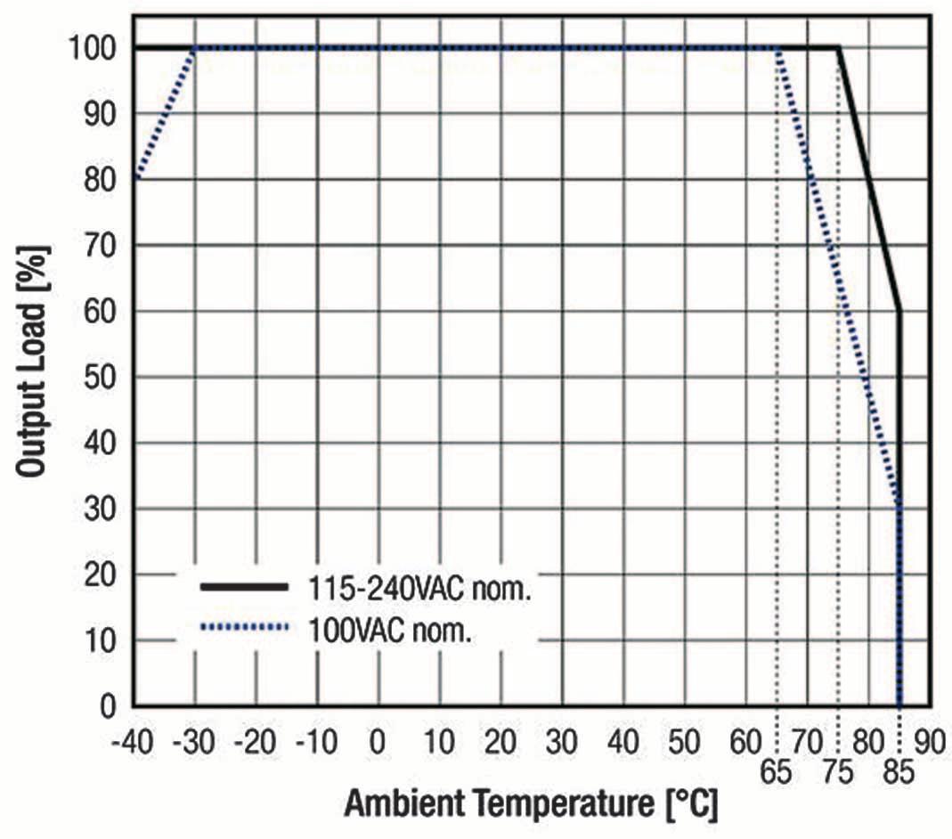
The 140% peak power capability of the 10-watt RAC10-05SK/277 5 volt dc output AC/DC power supply supports the transient power needs of systems with inductive, high start-up current or nonlinear loads such as process automation and smart building applications (Figure 5).
Fuses can be connected to both input lines if the ac input is not polarized. Typical fuse size recommendations for single-phase AC/DC power supplies are 1.5 amperes (A) for outputs under 40 watts, 2A for outputs over 40 watts but less than 60 watts, and 3A for outputs of 60 watts or more.
If the AC/DC power supply has a ground pin (FG), it must be earthed to a safety ground point. The -VOUT output voltage can be connected to FG, referencing the +VOUT output to ground. Designers should specify short, thick interconnects to guarantee solid connections to further reduce electromagnetic interference (EMI) (Figure 3).
These power supplies have a footprint of 1.45 inches by 0.95 inches and a low 15.4 millimeters (mm) profile.
Their 4 kV AC input to output isolation makes them suited for worldwide applications, and they meet the following standards:
• UL/IEC/EN62368-1 certified
• CAN/CSA C22.2 No. 62368-1 certified
• EN60335-1 (pending)
• EN62233 (pending)
• IEC/EN61558-1/2-16 (pending)
• EN55032/EN55035 compliant
The RAC03E-K/277 series devices have a wide operating temperature range, delivering full output power from -30 to +75°C (except for 3.3-volt output units which deliver full power to +70°C).
The 10-watt RAC10-05SK/277 AC/DC power supplies have international safety certifications for both industrial and household standards.
These printed circuit board (pc board) mounted AC/DC power supplies have international safety certifications for both industrial and household standards. The 10-watt models are available with single output voltages from 3.3 to 24 volts DC, or in dual output versions which deliver ±12 or ±15 volts DC. These power supplies meet IEC62477-1 power supply overvoltage category III (OVC III) for industrial systems used in fixed installations, and for cases where the reliability and the availability of the equipment is subject to special requirements. The power supplies in these installations typically have a permanent, hard-wired connection to the AC distribution panel.
a single input fuse is used (top), but if the input is not polarized, fuses can be placed in both input lines (bottom).© RECOM Power Figure 2 The
output voltage can be connected to Earth to reference the output to ground.Figure 3 © RECOM Power © RECOM Power Figure 5
POWER
Like the 3-watt RAC03E-K/277 discussed above, these AC/DC power supplies have an extra-wide input voltage range of 85 to 305 volts AC or 120 to 430 volts DC.
20-WATT POWER SUPPLIES WITH ULTRA-LOW NO-LOAD POWER Designers of IoT and smart devices can benefit from using the 20-watt RAC20-K series of AC/DC modules. For example, the RAC20-48SK version produces a 48 volt DC output with only 40 milliwatts (mW) of no-load power consumption in always-on and standby mode applications. These power supplies feature ErP Lot 6 Standby Mode Conformity. They are available with a wide input range of 85 to 264 volts AC, and an optional extra-wide input range of 85 to 305 volts AC or 120 to 370 volts DC.
• IEC/EN62368-1 certified
• UL62368-1 certified
• CAN/CSA-C22.2 No. 62368-1-14 certified
• IEC/EN60335 certified *
• IEC/EN61558-1 certified *
• IEC/EN61558-2-16 certified *
• IEC/EN61204-3 compliant *
• EN55032/14 compliant *
• EN55024 compliant *
TWO OUTPUTS FROM A SINGLE OUTPUT
As noted above, the 3-watt RAC03E-K/277 is only available in a single output design. The 10 watt RAC10-05SK/277 and the 20 watt RAC20-48SK AC/DC power supplies are offered with single and dual outputs. However, the dual output configurations are limited to ±12 or ±15 volts DC.
In some applications, a different combination of output voltages may be needed. In those cases, designers can pair a single output AC/DC power supply with a lower wattage DC/DC converter or switching regulator to deliver an auxiliary output voltage, or a negative output rail (Figure 7).
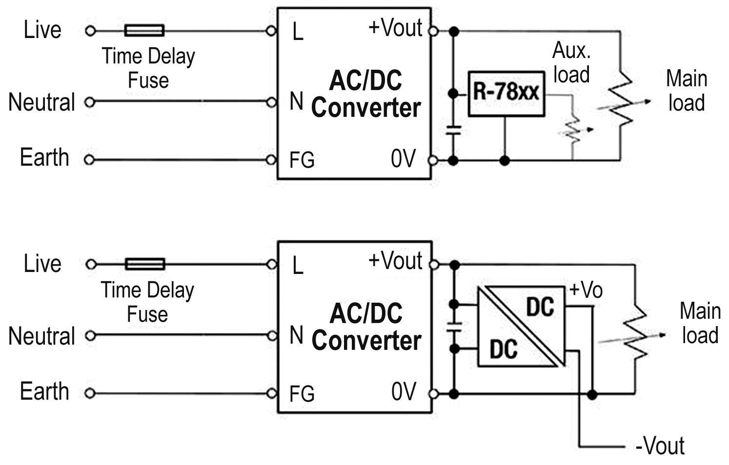
When an external filter is added, a central star-earth wiring topology should be used, and the cabling between the external filter and the converter should be as short as possible (Figure 8).
The need for low-wattage, board-mounted AC/DC power continues to grow, but they remain complex systems. If a designer isn’t well versed in the nuances of power supply design, test, and regulatory compliance, designing them from scratch can be time-consuming and can add cost, delay design schedules, and take up more board space than is necessary.
A better option in many instances is to choose from a number of off-the-shelf, compact, board mount AC/DC power supplies.
As shown, these come in a wide variety of input voltage ranges and can accept either AC or DC inputs. In addition, they are likely to already be certified to any relevant international performance standards and compliance regulations.
The efficiency versus output load plot for the RAC20-05SK (5-volt output model) shows high efficiency from light loads to full load.
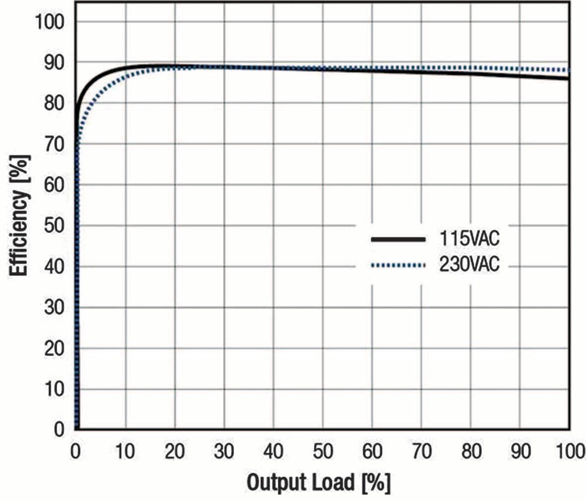
© RECOM Power
Modified versions of these power supplies meet IEC62477-1 power supply OVC III. These pc board mounted power supplies are available with single output voltages from 5 to 48 volts DC, or in dual output versions which deliver ±12 or ±15 volts DC.
These power supplies feature high efficiency from light loads to full load, as shown in the plot for the RAC20-05SK 5 volt version (Figure 6).
The RAC20-48SK AC/DC power supplies comply with EN 55022 Class B Conducted Emissions requirements without any additional filtering. They have an operating temperature range of -40°C to +85°C, and come with international safety certifications for industrial, audio visual and information technology equipment including (* = pending for the extra-wide input models):
The RECOM RAC series AC/DC power supplies discussed in this article all have a built-in line filter that meets EN 55022 Class B Conducted Emissions.
In more demanding applications additional filtering may be needed.
A switching regulator (R-78xx, on the top) or a DC/DC converter (bottom) can be combined with an AC/DC power supply to produce an auxiliary output voltage (top), or a negative voltage rail (bottom).
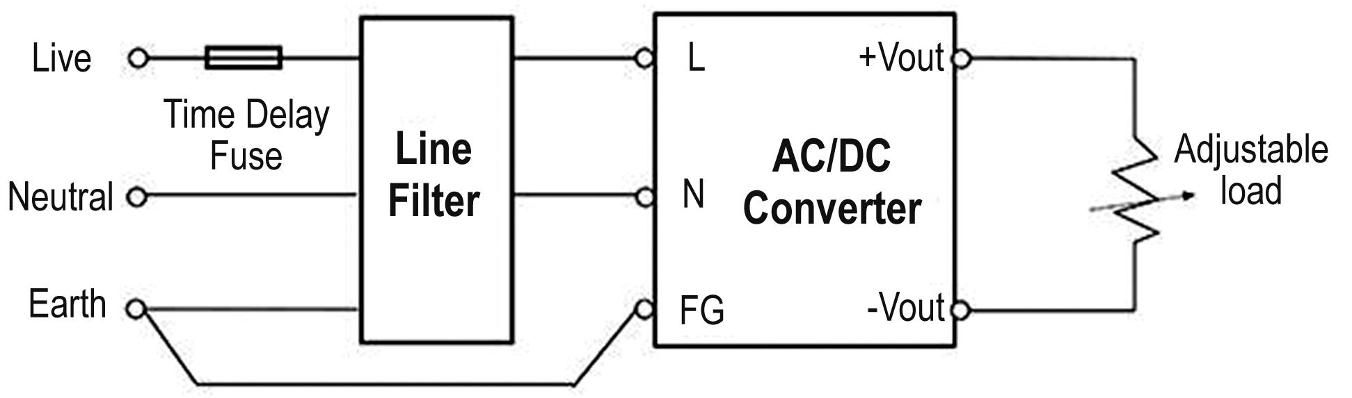
© RECOM Power
The RECOM RAC AC/DC power supplies meet EN 55022 Class B Conducted Emissions. An external filter can be added if needed.
© RECOM Power
Recommended reading
“A Guide to Selecting and Using IoT and IIoT Power Sources”
►Digi-Key Electronics
www.digikey.com

Infineon Technologies AG announced that its EZ-PD™ Power Adapter Generation 1 (PAG1) AC-DC power solution is used in the recently launched USB-C Fast Wall Charger from Verizon made by Xentris Wireless. The new Verizon charger powers on-the-go devices swiftly and provides up to 45 W of super-fast charging with compatible devices. The EZ-PD PAG1 is a twochip AC-DC power solution with integrated USB-PD functionality that enables compact chargers. These powerful chargers work with all USB-C charging cables and charge both state-of-the-art and legacy devices that have USB-C ports.
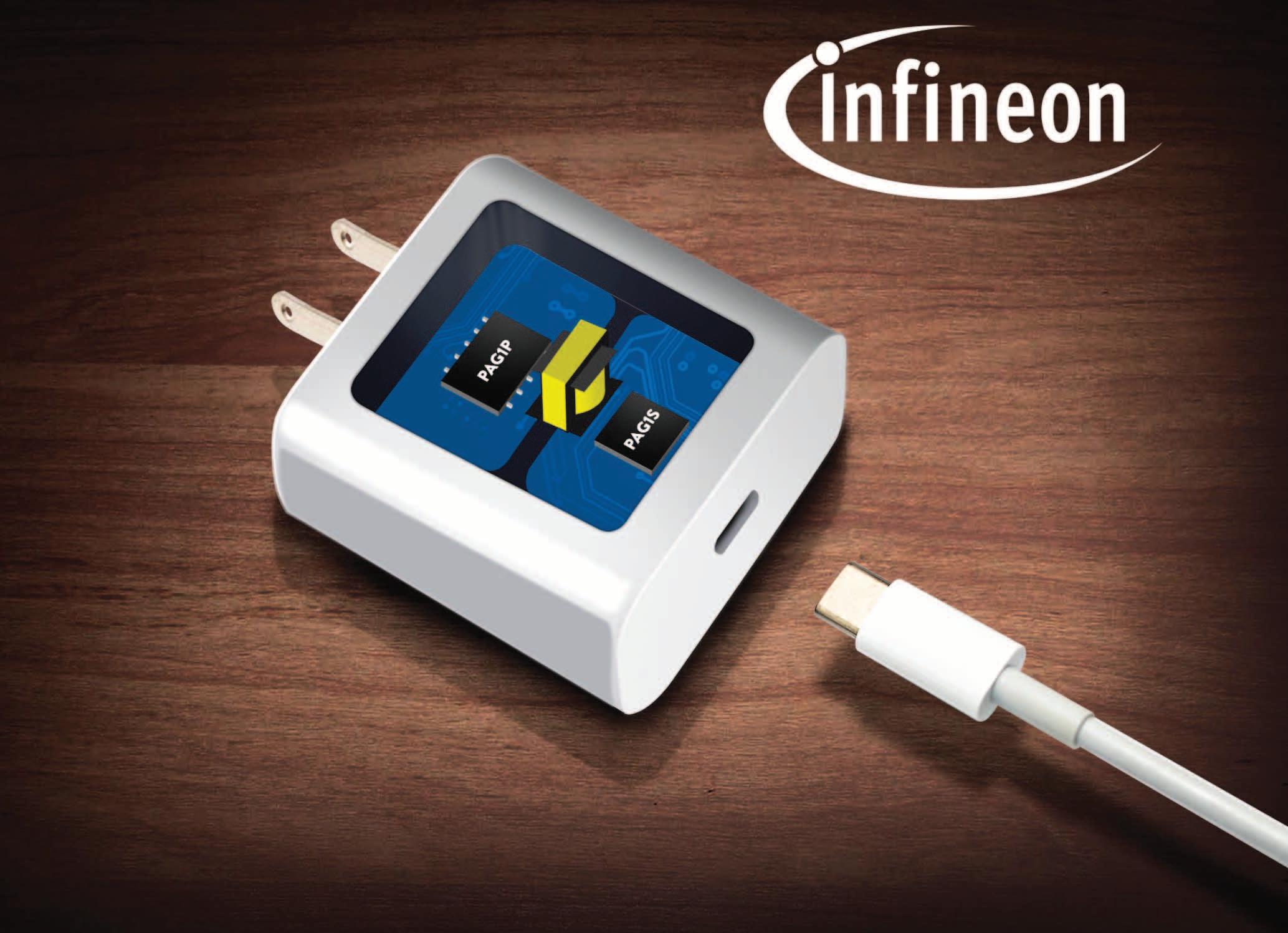
“The EZ-PD PAG1 chipset is the ideal choice for a high-performance AC-DC wall charger including secondary rectification and a PD controller,” said David Bailey, CEO of
Xentris Wireless. “This all-in-one solution made it possible to significantly reduce the printed circuit board footprint and bill of materials, allowing us to pack more power into a smaller charger, which is ideal for our on-the-go customers who demand fast charge times for their devices.”
Infineon’s EZ-PD PAG1 family of primary and secondary controllers provides a unique combination of secondary-side control and high levels of integration to enable high-density designs with both gallium nitride ( GaN ) and silicon ( Si ) power transistors.
These integrated features enable system designers to bring more differentiated chargers to market while reducing their overall bill of materials (BOM) for designs with power levels from 18 to 65 W.
“We are excited to team with Xentris Wireless on their recently launched USB-C Fast Charger,” said Ajay Srikrishna, Senior Vice President and General Manager of the Wired Connectivity Solutions Product Line at Infineon. “We are committed to collaborating closely with customers such as Xentris Wireless to enable them to bring highly differentiated solutions to market while simplifying product design and supply chain management, and the EZ-PD PAG1 chipset does just that.”
The Infineon EZ-PD PAG1 devices are available now. More information is available at: https://www.cypress.com/products/pag1-power-adapter-generation-1.
Infineon Technologies
https://www.infineon.com

Extracting clean energy from water has been a dream for more than a century and many of us remember the book Jules Verne wrote in 1874, ‘The Mysterious Island’ and its vision to extract hydrogen from water, it becoming an infinite source of energy for future generations. So, for 147 years, the use of civil hydrogen has been up for debate and we are unable to hazard a guess at the number of articles, conferences and announcements supporting the inception of hydrogen as an undoubtable source of energy.
Author: Patrick Le Fèvre Chief Marketing and Communication Officer Powerbox a Cosel Group Company

For us as power electronics engineers, very much as it was in Jules Verne’s vision, hydrogen energy is achieved by electrolyzing hydrogen and oxygen, and then deploying a fuel cell to generate electricity. In reality the worldwide production of hydrogen by electrolyzation is less than
4%, with more than 94% produced from fossil resources, mainly coal and gas, and with anecdotal production from biomass and other representing just 2%.
70% of the overall hydrogen produced in the world is extracted from the natural gas methane. Its extraction uses a so called
‘steam reforming’ process in which hightemperature steam (700°C – 1,000°C) is used to produce hydrogen. The steam reforming process, if the CO2 is not captured is responsible of high levels of greenhouse gas emissions. The amount of CO2 released by worldwide hydrogen production is estimated to be around 830 million tons of carbon dioxide released into the atmosphere. This is where we are today, with the conundrum ‘green hydrogen - myth or a reality’ fuelling the debate. But things are changing and we are getting closer and closer to Jules Verne’s vision!
To simplify the understanding of the different production methods and their environmental impact, industry has codified hydrogen by colour. In practice, four main categories are commonly used; brown, grey, blue, and green. From timeto-time sub-categories appear e.g., the hydrogen that is produced by electrolyzers powered by nuclear plants is sometimes referred to as ‘pink’, but that is more anecdotal than a de facto delineation.
The color brown has been assigned to hydrogen extracted from coal by gasification. In this process the carbon-based material is converted into a mix of carbon monoxide, hydrogen, and carbon dioxide. Gasification is achieved at very high temperatures (>700°C) without combustion with a controlled amount of oxygen and/or steam. The carbon monoxide then reacts with water to form carbon dioxide and more hydrogen via a water-gas shift reaction. The resulting gas from this process is called syngas. The hydrogen produced by this method is known as brown (lignite) or black (bituminous) depending on the type of coal used. However, this process is highly polluting since both the CO2 and carbon monoxide cannot be reused and are released into the atmosphere.
Nowadays, grey hydrogen represents the highest portion of production. More than 70% of hydrogen currently produced worldwide is classified as grey hydrogen. The most common production process uses steam methane reforming (SMR). In this process high pressure steam reacts with methane resulting in hydrogen and the greenhouse gas CO2 In this process about 9.3kg of CO2 per kg of hydrogen is generated, which is lower than brown hydrogen although still a substantial amount when released into the atmosphere.
When CO2 produced from the previous methods is captured and stored underground using industrial carbon capture and storage ( CSS ) the manufacturing process is less harmful for the environment, though it is more expensive and less efficient than conventional methods. Blue hydrogen is considered an important step in the energy transition towards green hydrogen and the vast majority of new production units are strictly controlled in terms of their environmental impact. However, despite high levels of improvement, compared to brown and grey, 10 to 20% of the CO2 cannot be captured and is released.
Globally, the amount of hydrogen production from water electrolysis is very small, less than 4%, but it is the most well-known technique, one that some of us will remember from our school chemistry lessons. Using electricity, hydrogen is produced by splitting H2O molecules into hydrogen and oxygen. In the case of green hydrogen, the electricity is produced by renewable energy sources (less than 1%). In the process the electrolyzers are the ‘masterpiece’ and have been used for decades with an average efficiency of 73% (compared to 65% for the steam reforming process). As for the power supply, improving its efficiency is obviously vitally important to reduce energy consumption and cost. Worldwide, intensive research aims to achieve a 95% conversion efficiency, which in fact we are not far away from achieving.

We are all aware of climate challenges and the Paris agreement adopted on December 12, 2015 by 196 Parties at COP 21 in Paris. The ratified agreement was entered into force on 4 November 2016. The Paris Agreement embraces a vision of fully utilizing the development of technology and transfer for both improving resilience to climate change and reducing greenhouse gas emissions.
In their response to challenges relating to climate changes, in December 2019 the European Commission communicated the so-called ‘European Green Deal’, aiming to transform the EU into a fair and prosperous society with a modern, resource-efficient and competitive economy where there are no net emissions of greenhouse gases in 2050 (figure 1). The European Green Deal is also the lifeline out of the COVID-19 pandemic. One third of the 1.8 trillion euro investments from the ‘NextGenerationEU’ recovery plan, and the EU’s seven-year budget will finance the European Green Deal.
To achieve this goal many activities have been initiated and one of those is to develop and deploy a European strategy for hydrogen. This strategy was published in July 2020, setting out a vision of how the EU can turn clean hydrogen into a viable solution to decarbonize different sectors over time, installing at least 6GW of renewable hydrogen electrolyzers in the EU by 2024 and 40GW of renewable hydrogen electrolyzers by 2030.
To support that strategy, it is important to have global coordination between public authorities, industry, civil society and the research community. A number of alliances were formed, facilitating synergies and the execution of strategies.
As part of the New Industrial Strategy for Europe, in July 2020 the European Clean Hydrogen Alliance (ECH2A) was launched in the context of the hydrogen strategy for a climate-neutral Europe.
The European Clean Hydrogen Alliance is aimed at developing and deploying hydrogen as a viable and competitive energy carrier in Europe. The Alliance supports the implementation of the hydrogen strategy for a climate neutral Europe, by working towards developing a full and accessible EU wide hydrogen value chain. This will be achieved through, among others things, an investment agenda and a pipeline of projects, as well as by mobilizing resources and actions to install renewable hydrogen electrolyzers to achieve the aforementioned 6GW and 40GW objectives.
In April 2021 the EU Commission sent an invitation to all 1000+ members of the European Clean Hydrogen Alliance inviting them to submit projects for renewable
and low-carbon hydrogen technologies and solutions. In June 2021 the second European Hydrogen Forum took place and reported an impressive number of 1,052 submitted projects, from which 997 met the eligibility criteria. This number reflects the very high engagement of European industry to accelerate the development of hydrogen in Europe.
Materials & New Production Technologies’, ‘Environment (including Climate Change)’, and ‘Transport (including Aeronautics)’. Amongst the projects and initiatives, we should mention one very interesting study, commissioned by Clean Sky 2 and Fuel Cells & Hydrogen 2 Joint Undertakings on hydrogen’s potential for use in aviation.
Because the importance of developing efficient electrolyzers is a high priority, as long ago as 2003 the European Commission facilitated the creation of the European Hydrogen and Fuel Cell Technology platform with the goal to link public and private research and create initiatives to accelerate the development of efficient fuel-cell and hydrogen technologies.
From this initiative, in May 2008 the Council of the European Union set up the Fuel Cells and Hydrogen Joint Undertaking (FCH JU) with the objective: To contribute to the implementation of the Seventh Framework Program and in particular the Specific Program ‘Cooperation’ themes for ‘Energy’, ‘Nanosciences, Nanotechnologies,
Sweden / Mariestad ElectriVillage solar to hydrogen autonomous station
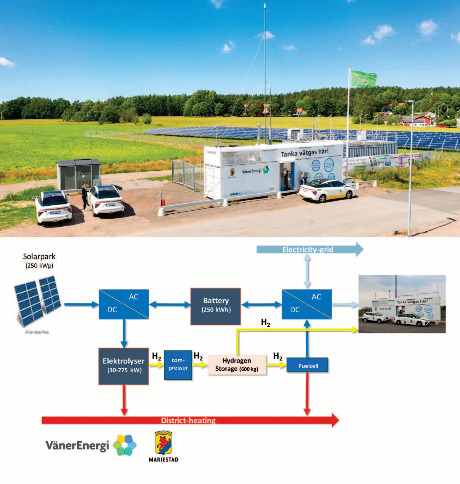
Using hydrogen in aeronautics will require a huge amount of technical innovation and a new infrastructure, but it is seen as a major step forward in the reduction of CO2 emissions from the aviation sector. The airplane manufacturer AIRBUS took part in the study and it’s worth mentioning the company’s ambition to develop the world’s first zero-emission commercial aircraft by 2035 (figure 2).
Step by step, slowly but surely, green hydrogen is becoming a reality and the number of installed electrolyzers is rapidly increasing. Clearly it would be difficult to list all the projects, but it’s interesting to mention a few of them to illustrate the reality.
Located in the southern part of Sweden on the shore of the lake Vänern, the municipality of Mariestad developed a concept to create a sustainable energy ecosystem based on renewable energy and hydrogen. The original project included a large array of solar panels to power electrolyzers generating hydrogen for an autonomous refuelling station for cars and utility vehicles. Exploring the large range of possibilities offered by this technology, the station could also use the stored hydrogen to supply a fuel cell to generate electricity. The oxygen resulting from the split process in the electrolyzers is captured and stored for medical, industrial or farming applications.
This autonomous station is a good example of what could be deployed at a larger scale and even to generate hydrogen for other vehicle such as local trains (figure 3).

As part of the REFHYNE European consortium and with EU funding through the Fuel Cells and Hydrogen Joint Undertaking (FCH JU), the largest European polymer electrolyte membrane (PEM) water electrolyzers began operating at Shell’s Energy and Chemicals Park in Rhineland near Cologne.

After decades of interest in hydrogen, we have finally entered a new era. Europe began its ‘H’ engagement more than 20 years ago and the ‘Green Deal’ boosted research, cooperation and deployment. There is no doubt that Europe has taken major steps to reach the 2050 goal and other countries are also speeding-up their hydrogen strategies. In the US under Joe Biden’s impulse, major activities are taking place.
As announced on July 7, 2021 by the U.S. Department of Energy (DOE), an allocation of $52.5 million will fund 31 projects to advance next-generation clean hydrogen technologies and support DOE’s recently announced Hydrogen Energy Earthshot initiative to reduce the cost and accelerate breakthroughs in the clean hydrogen sector. These are clear signs that hydrogen is an important part of US energy transition strategy.
Hydrogen is no longer a myth and Jules Verne’s vision: “Water will one day be employed as fuel, that hydrogen and oxygen which constitute it, used singly or together, will furnish an inexhaustible source of heat and light, of an intensity of which coal is not capable” will become a reality.
The Rheinland electrolyzers will use renewable electricity to produce up to 1,300 tons of green hydrogen a year, and plans are underway to expand capacity of the electrolyzers from 10 megawatts to 100 megawatts (figure 4).
These two examples reflect the scale of hydrogen initiatives in Europe and especially considering the large number of projects, place Europe as a leading player in energy transition and industry decarbonization.
►Powerbox www.prbx.com
References
• Powerbox (PRBX): https://www.prbx.com


• EU Green Deal: https://ec.europa.eu/info/strategy/priorities-2019-2024/european-green-deal_en
• EU Hydrogen: https://ec.europa.eu/energy/topics/energy-system-integration/hydrogen_en
• EU Clean Hydrogen Alliance https://www.ech2a.eu/
• EU Fuel Cells and Hydrogen Joint Undertaking: https://www.fch.europa.eu/

• Mariestad ElectriVillage (Youtube video): https://youtu.be/ryfOEIqQTco?list=PLT-QkyUkOkuuT_PZU-QBx40juY6jmWva1

• AIRBUS ZEROe: https://www.airbus.com/innovation/zero-emission/hydrogen/zeroe.html
• Germany – Wesseling REFHYNE PEM Electrolyser plant: https://www.shell.com/energy-and-innovation/new-energies/hydrogen.html
Based on a robust platform, the PJMA’s design has been optimized to offer a very good price/performance ratio for medical applications requiring a high quality power solution https://www.coseleurope.eu/Products/AC-DC/PJMA
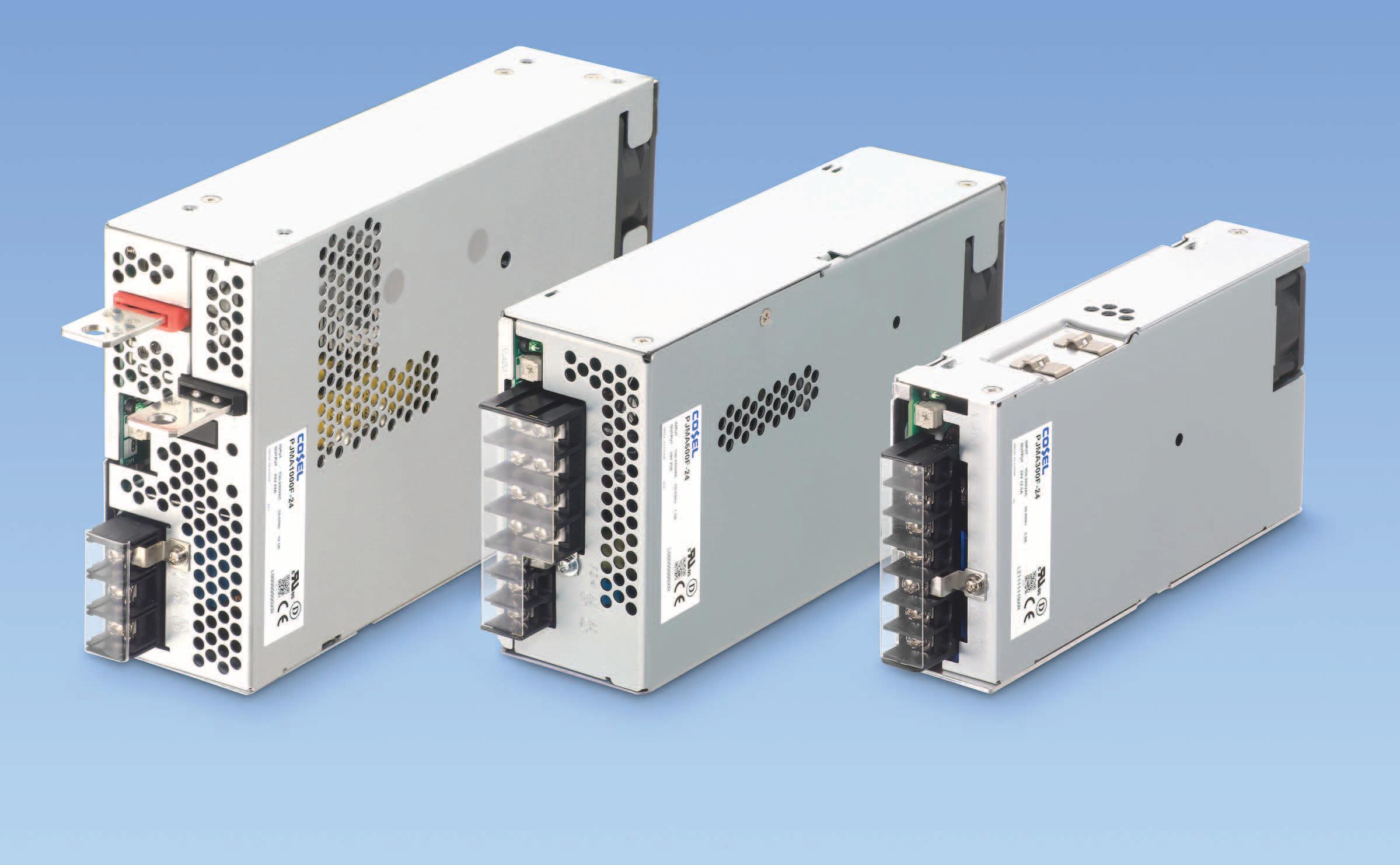
COSEL Co, Ltd announced the expansion of its medical power offering with the addition of a 300W version to its PJMA series. The 300W PJMA300F have a universal input range of 85 to 264VAC and comply with international safety standards. Designed for demanding medical applications, the PJMA series is suitable for Body Floating (BF) applications and complies with 2MOPP (IN/OUT) and 1MOPP (OUT/FG) safety requirement. Based on a robust platform, the units’ design has been optimized to offer a very good price/performance ratio for medical applications requiring a high quality power solution. The PJMA series is available in four output voltages of 12, 24, 36 and 48VDC.
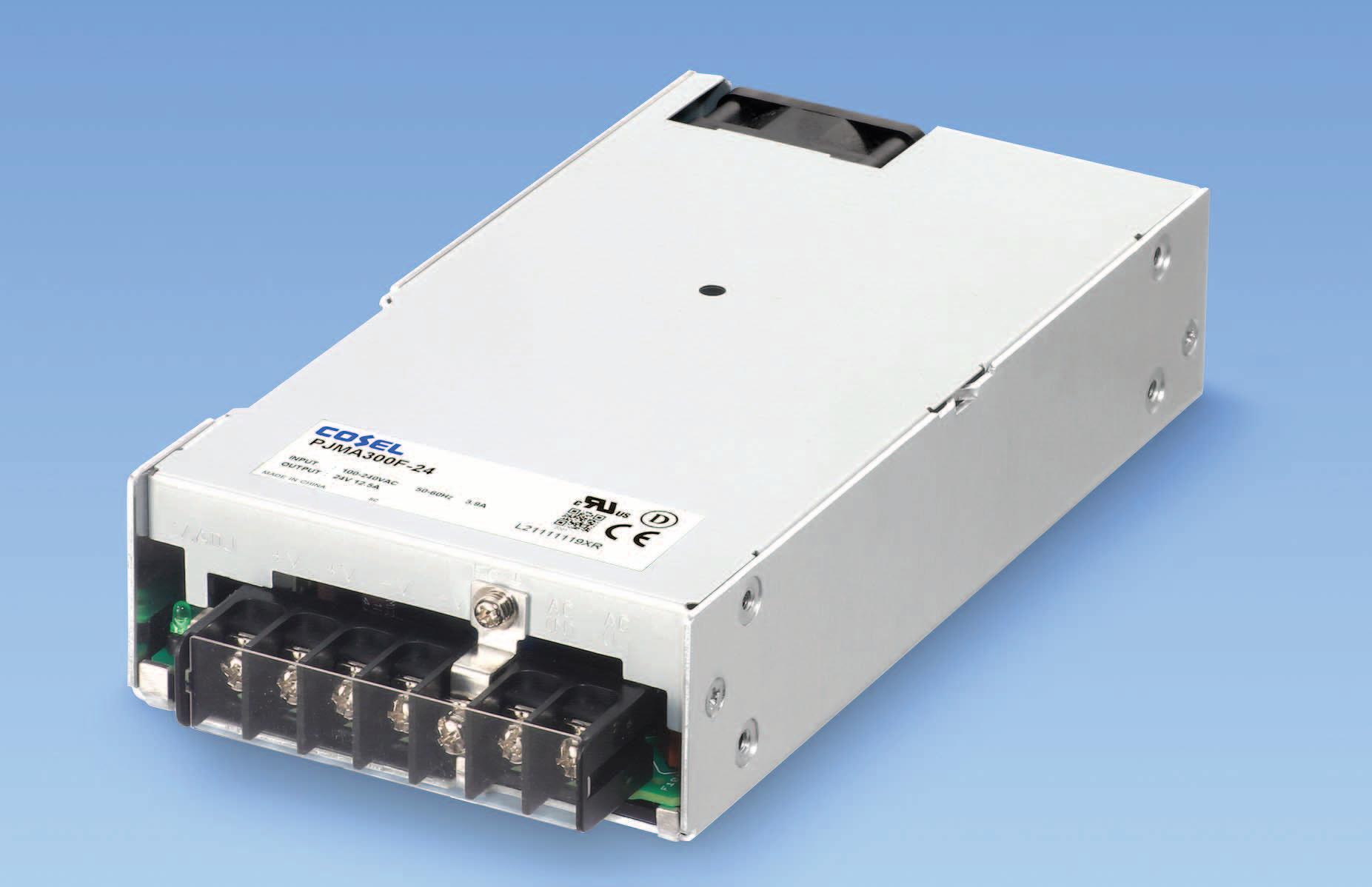
Medical applications are requiring robust and highly reliable power supplies that are able to operate around the world and comply with safety regulations. Based on many years of expertise, COSEL power designers developed an optimized platform to offer an excellent price/performance ratio without compromising on quality and reliability. The PJMA series can be operated within the so called ‘uni-
versal Input’ range of 85 to 264VAC, and has a typical efficiency of 86% at high line. Four single output voltages are available as standard, 12V/25A, 24V/12.5A, 36V/8.4A, and 48V/6.3A. The output voltage can be adjusted by using the built-in potentiometer. The PJMA series includes inrush current limiting circuitry, overcurrent and overvoltage protection, as well a thermal protection. Exhibiting versatility and robustness, the power supplies can be operated in an environmental temperature range of -20 to +70°C. Depending on the final equipment assembly style and cooling conditions, a derating may apply. With its medical focus, the PJMA series input to output isolation complies with 2MOPP, its input to ground with 1MOPP, and output to ground with 1MOPP. The units are approved in accordance with ANSI/AAMI ES60601-1 and EN60601-1 3rd Edition.
In conducted emission tests, the PJMA series complies with the FCC-B, CISPR11-B, CISPR32-B, EN55011-B, EN55032-B, and VCCI-B. For applications requiring even lower emission levels an additional filter COSEL
type NAC can be supplied (NAC-06-472).
To accommodate application specific requirements, a number of options are available including conformal coating (C), low leakage current (G), external potentiometer connector (V), remote control (R), and low speed fan (F4).
For strength and longevity, the PJMA series is built in an enclosed, galvanized steel box with a fan mounted on the rear side. The PJMA300F measures 102 × 41 × 190mm [4.02 × 1.61 × 7.48 inches] (W × H × D), and has a weight of 1.0 kg max.
Cosel Group
https://www.coseleurope.eu
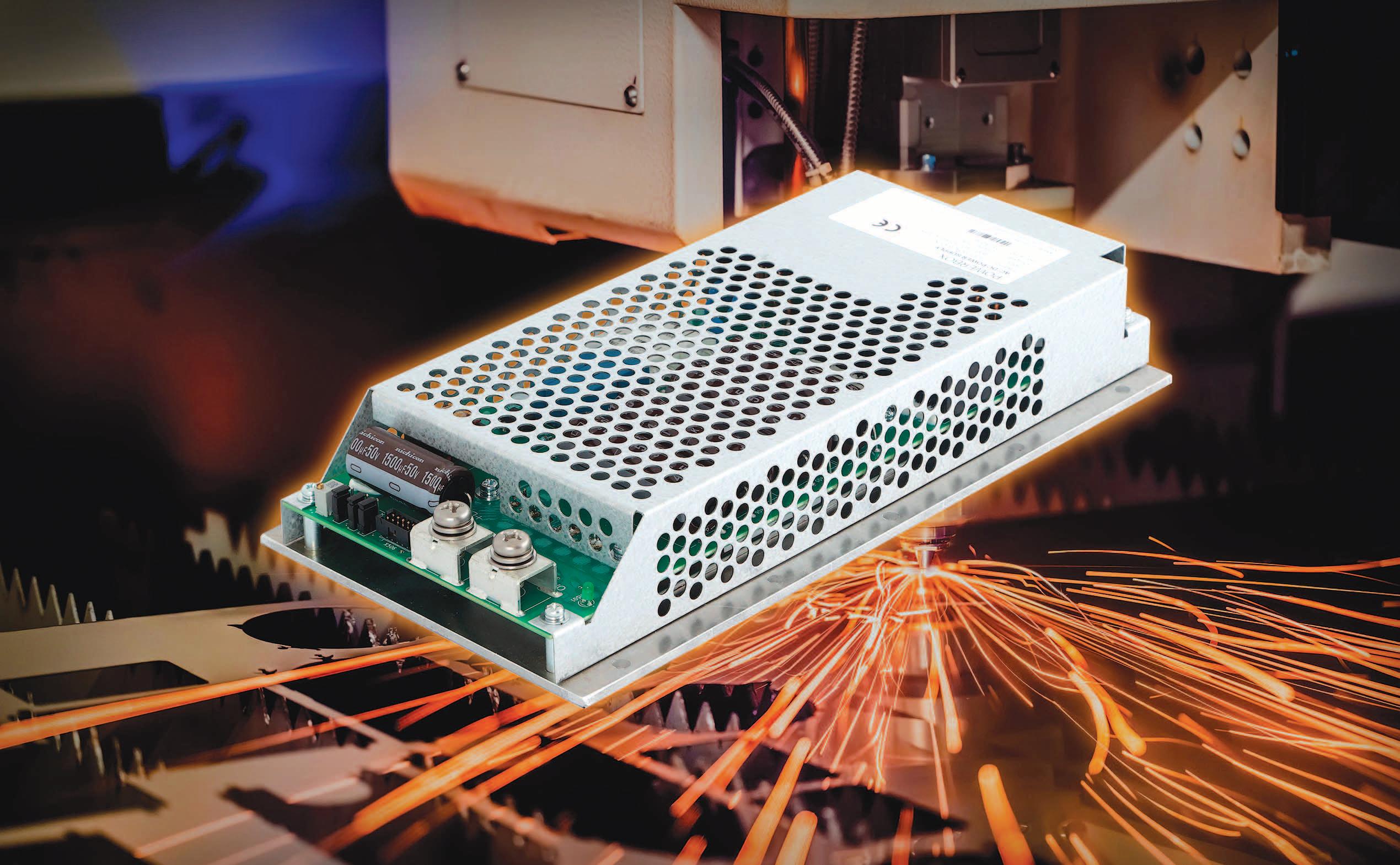
Powerbox has announced the release of a new 700W power supply for industrial applications, the OFI700A. Optimized for conduction cooling, the OFI700A delivers high performance levels across a baseplate temperature range of -40 to +95°C, without the use of a fan. The power supply operates with a wide universal input range from 85 to 264VAC with power factor correction (PFC) and is available with DC outputs of 12V, 28V (adjustable to 24V) or 48VDC. A 12V auxiliary is also provided. In many industrial applications cooling of the dissipating elements relies on the use of fans and blowers. But there are applications where it is not possible or even allowed to use active ventilation. In harsh environments or in applications where the required reliability level imposes the need to remove all possible risk of failure, fans and blowers are not allowed. A sealed box such as is required for laser-cutting is but one example, but there is also a growing demand for equipment installed in supervisory rooms or even offices that for the comfort and health of the employees, generated noise is simply not allowed or needs to be very much limited. Conduction cooling requires very specific building practices and the PRBX OFI700A
has been designed to guarantee optimal heat transfer from the dissipating components to the baseplate, delivering a high level of performances within an operating temperature of -40 to +95°C at baseplate. Depending on the assembly method and the overall cooling conditions, a derating may apply as specified in the technical documentation.

To cover a wide range of applications, the OFI700A operates with a wide universal input range from 85 to 264VAC. The unit includes a PFC with a coefficient of 0.95/0.92 (110VAC/230VAC). For applications powered by a DC bus e.g., mining equipment, the OFI700A operates from 120 to 350VDC.
The OFI700A is available in three versions of single output DC voltage, 12V/58.4A ; 28V/25A and 48V/14.6A. The output voltage can be adjusted using the provided onboard potentiometer. For example, the 28V output can be adjusted from 22.4V to 33.6V, covering the 24V applications. An additional voltage of 12V/0.1A is provided for auxiliary functions. For applications requiring 1+1 redundancy it is possible to connect two units in parallel, adding an external diode to protect the unit. Using a diode for this purpose is
a simple solution but it increases power losses which depending on the output current could be as high as 30W. So, to maintain the highest level of efficiency when operated in redundancy-mode, an ‘option O’ OFI700A version is available with active ORing circuitry deploying high performance FET technology. In this version the power losses are minimized to an excellent less than 1.5W.
For safety, the OFI700A has an IN/OUT isolation of 3,000VAC and IN/FG of 2,000VAC. Output isolation to FG is 500VAC. The power supply includes over current protection with auto recovery, over voltage and over temperature protection. The OFI700A board includes easy access to auxiliary functions via on board connectors, namely: Remote Control, Output Voltage Sensing, DC-OK, Inverter Operation Mode (IOG) and auxiliary 12V. The OFI700A has endured shock and vibration testing as specified in MIL-STD-810H. In that respect the products have been tested to levels far above normal operating conditions and are specified to sustain a high 20G vibration level during transportation.

As the Linux open-source operating system marks its 30th anniversary, Analog Devices, Inc. (ADI) announces the expansion of its Linux distribution by recognizing over 1000 ADI peripherals supported by in kernel Linux device drivers. Designed to enable the rapid development of embedded solutions, these open-source device drivers streamline the software development process for ADI’s customers, providing access to tested, high-quality software to create innovative solutions across a range of industries, including telecom, industrial, military, aerospace, medical, automotive, security, Internet of Things (IoT), consumer, and more. This portfolio includes products from Maxim Integrated Products, Inc., now part of Analog Devices.
Analog Devices also released “Kuiper Linux,” a free Linuxbased operating system based on Raspbian/Debian that is optimized for ADI peripherals and supports popular ARMbased systems such as Raspberry Pi, Xilinx Zynq, Xilinx Zynq Ultrascale+ MPSoC, Intel Cyclone V SoC, Intel Arria 10 SX SoC, and Intel Stratix 10 SoC. The new Linux distribution focuses on ensuring ready-to-use in kernel Linux device drivers, offering embedded customers a robust system for software development, reducing risk and development time with pre-existing code that is peer-reviewed and industry backed. The distribution contains all the essential components for running the built-in drivers and enables customers to integrate custom software. By providing both hardware and software compatibility across the customers’ full ecosystem, the Linux distribution will help prevent hardware lock-in, while also minimizing software development needs.
Learn more about ADI’s Linux Kuiper distribution and drivers:
• Linux code: https://github.com/analogdevicesinc/linux
• Supported devices & documentation: https://wiki.analog.com/linux
• Linux support: https://ez.analog.com/linux-software-drivers
►Analog Devices | https://www.analog.com
MicroSys miriac AIP-S32G274A SBC with Hailo-8 AI accelerator modules
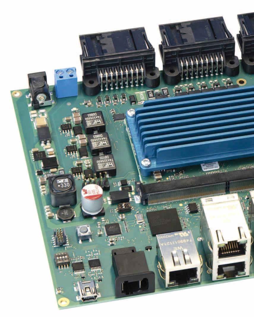
NXP Gold partner MicroSys Electronics announced that its new embedded SoM (System-on-Module) platform miriac AIP-S32G274A, which is based on NXP S32G vehicle network processors, now supports Hailo-8 AI accelerator modules. A result of MicroSys’s partnership with leading AI (Artificial Intelligence) chipmaker Hailo the powerful AI solution delivers up to 52 TOPS (tera operations per second) for ASIL D safe zonal gateways and real-time controls in autonomous vehicle and stationary machine applications. The new, applicationready SoM based AI platform targets a wide range of industrial and mobility markets such as Industry 4.0 gateways, zonal automotive controllers, ADAS (Advanced Driver Assistance System) controllers, heavy machinery controls, smart farming robots, autonomous logistics vehicles, robots and more, and meets OEM requirements in terms of industrial quantity, quality and long-term availability.
Powered by the NXP S32G274A vehicle network processor, the SoM based miriac AIP-S32G274A can integrate up to 2 advanced Hailo-8 AI accelerators to reach its maximum AI performance of 52 TOPS, providing best-in-class processing performance and deep learning capabilities for decentralized situational awareness. The embedded platform delivers exceptional AI computing performance across multiple standard NN benchmarks, including 2450 Frames Per Second (FPS) on Resnet-50, 2100 FPS on Mobilenet-V1 SSD, and up to 380 FPS on YOLOv5m.
Awarded “Best AI and Vision Processor 2021” by the Edge AI and Vision Alliance, the automotive grade Hailo-8 outperforms other available AI processors for edge computing with up to 26 TOPS at a typical power consumption of 2.5 W. The miriac AIP-S32G274A embedded platform, combining the Hailo-8 AI processor with MicroSys’s Arm Cortex NXP Automotive S32G platforms, provides customers with a highly efficient way to implement AI into their connected edge appliances.
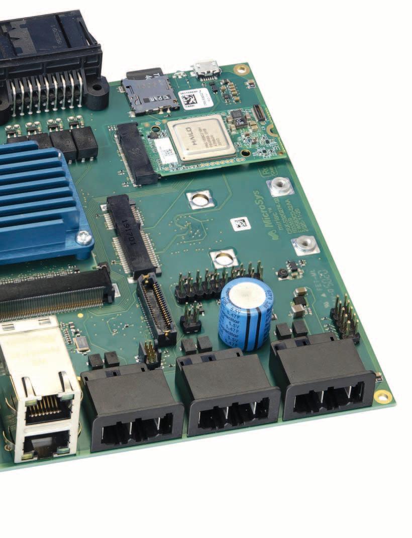
The new application-ready miriac AIP-S32G274A starter kit for AI is a highly effective springboard for cost efficient custom designs in industrial quantity, quality and long-term availability and comes complete with everything necessary for evaluation and development. It includes an IEC 61508 compliant and ASIL D safety ready miriac MPX-S32G274 SoM with quad Arm Cortex-A53 cores plus triple Arm Cortex-M7 dual-cores, 1 or 2 Hailo-8 AI processor modules, a carrier board with Ethernet with TSN, PCIe, USB, SPI, and I2C as well as standard automotive busses like Flexray (2x), LIN (4x) or CAN (16x plus 2x CAN FD) and a cable set. Developers also have access to the comprehensive AI and development tools offered in the Hailo Developer Zone. More information about the miriac AIP-S32G274A: https://www.microsys.de/en/products/system-device/offthe-shelf/miriac-aip-S32G274A
More information about the miriac MPX-S32G274 SoM: https://www.microsys.de/en/somnxps32g
Hailo, an AI-focused, Israel-based chipmaker, has developed a specialized AI processor that delivers the performance of a data center-class computer to edge devices. Hailo’s processor is the product of a rethinking of traditional computer architecture, enabling smart devices to perform sophisticated deep learning tasks such as object detection and segmentation in real-time, with minimal power consumption, size, and cost. The processor is designed to fit into a multitude of smart machines and devices, impacting a variety of sectors including automotive, Industry 4.0, smart cities, smart homes, and retail. For more information visit https://www.hailo.ai
►MicroSys Electronics | https://microsys.de
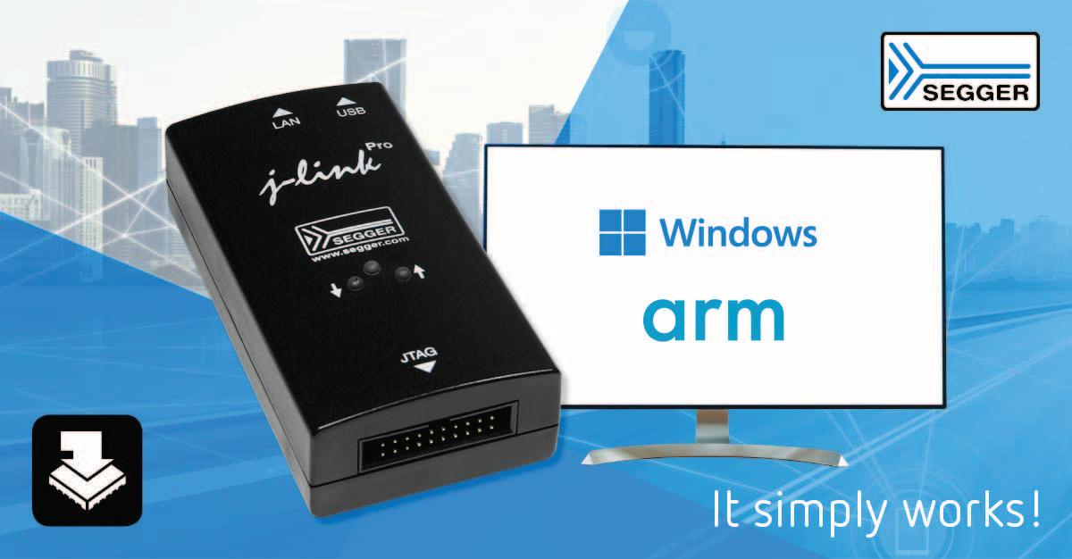
The software in the new package runs natively on Arm processors, ensuring that no performance or power is lost in emulation. Using J-Link and J-Trace with Windows on Arm looks and feels the same as working on an Intel/AMD-powered computer. The new package contains the same components as the JLink suite of software available for other operating systems and provides identical functionality. This includes command-line programs as well as GUI tools such as J-Flash, JFlash SPI, J-Scope, the J-Link Configurator and the GUI version of the SEGGER GDB Server.
“SEGGER products have been multi-platform for many years,” says Rolf Segger, founder of SEGGER. “J-Link software now runs on any combination of Linux, macOS and Windows on Intel/AMD or Arm. Our Embedded Experts do an outstanding job of swiftly adapting to emerging trends and technology. They have proven once again that SEGGER products are truly future-proof. Ease of use, robustness, unparalleled performance, direct download into flash memory, an unlimited number of breakpoints in flash memory, and compatibility with all popular environments, just to name a few, make J-Link an unbeatable choice.”
SEGGER tested J-Link software with Windows on Arm natively using a Microsoft Surface tablet and a Raspberry Pi, as well as in a virtual machine on an Arm-powered M1 Mac.
About J-Link
SEGGER J-Links are the most widely used line of debug probes on the market. J-Link opens the door to all major development tools, from commercial toolchains to GDB-driven ones. With features such as Real-Time Transfer (RTT) for interactive user I/O in embedded applications and High Speed Sampling (HSS) for data acquisition, J-Link is a key component of third-party utilities that provide real-time system tracing and inspection. With J-Link comes many utilities such as the J-Link GDB Server and J-Scope for real-time time data visualization.
The J-Link software package also comes with J-Flash, a production-grade programming software, and Ozone, the J-Link debugger (J-Link PLUS or higher).
Also available is SEGGER Embedded Studio for generating, downloading and debugging programs using J-Link.
For additional information about J-Link, please visit: https://www.segger.com/products/debug-probes/j-link/ ►SEGGER | https://www.segger.com
Good air quality is an important component of a healthy indoor environment because indoor air pollution can have harmful impacts on our health. There are many potential and common dangers found in indoor air, such as VOCs (volatile organic compounds), which are typically found in building materials, furniture and cleaning products, among others, and are emitted by humans, and NOx (nitrogen oxides), which are a by-product of combustion. Exposure to these pollutants can be limited by ensuring that enclosed spaces have sufficient ventilation. In addition, air treatment devices are used to eliminate harmful gases in indoor environments and thus avoid unhealthy situations. Equipped with Sensirion’s new SGP41, air purifiers become smart by reliably monitoring VOCs and NOx at all times and removing these gas emissions automatically when the appropriate filters are installed.
The VOC+NOx sensor offers a solution for two complete sensors on a single chip, facilitating design-in and cutting design costs. By relying on Sensirion’s proven MOXSens® Technology, the sensor’s unmatched robustness against contamination by siloxanes results in outstanding long-term stability in terms of sensitivity and response time. The two sensor signals processed by Sensirion’s powerful Gas Index Algorithm can be used directly to automatically trigger the removal of indoor air gas pollutants by air treatment devices without the need for user-device interaction. This sensor solution is thus well-suited to the constant monitoring of VOC and NOx levels, including potentially harmful events that are imperceptible to humans. Furthermore, automatic control of air treatment devices based on the SGP41’s signals helps to save energy by turning them off once the VOC and/or NOx events have been taken care of.
“This sensor platform enables the simultaneous measurement of both volatile organic compounds and nitrogen oxides, and therefore responds to the growing awareness of the importance of good indoor air quality and the stricter requirements for these applications. With the SGP41, Sensirion aims to further improve indoor air quality and help to protect our health and well-being,” says Dr. Oliver Martin, Product Manager for Gas Sensors at Sensirion.
For more information about the SGP41 VOC+NOx sensor, please visit: https://www.sensirion.com/sgp41
Explore the capabilities of the SGP41 with the SEK-SVM4x evaluation kit and visit https://www.sensirion.com/my-sgp-ek
►Sensirion | https://www.sensirion.com
Less susceptible to interference: the XENSIV™ PAS CO2 sensor uses the principle of photoacoustic spectroscopy (PAS), which enables a significant reduction in form factor and at the same time a lower purchase price.
Since PAS, in contrast to the established NDIR technology, dispenses with a large number of optical components, the sensor’s susceptibility to interference is reduced. The combination of a small form factor (13.8 × 14 × 7.5 mm) and SMD technology enables easier integration into volume applications. The
Particularly accurate measurement with reduced form factor: XENSIVTM PAS CO2 sensor from
VOC+NOx sensor for indoor air quality applications is now available worldwide
XENSIVTM PAS CO2 is ideally suited for use in demand-controlled ventilation systems, air conditioning and air purifiers, indoor air quality monitors, CO2 ventilation alarms and emission controls, and IoT / smart home / smart city management. The Infineon range is available at www.rutronik24.com. Using advanced compensation and self-calibration algorithms, the sensor has a durable and consistently high measurement quality. The accuracy for measurements in a range from 0 to 10,000 ppm (specified) is ±30 ppm or ±3 percent of the measured value.
The Xensiv™ PAS CO2 Sensor2Go Evaluation Kit and the Xensiv™ PAS CO2 Mini Evaluation Board are two development components provided by Infineon. The Sensor2Go evaluation kit impresses with simple plug&play via micro-USB cable, whereas the Mini Evaluation Board is a low-cost way to integrate the sensor on development boards using a standard pin header.
Further features
• Voltage range: 12 V (emitter) and 3.3 V (other components)
• Power consumption: 30 mW @ 1 measurement per minute
• Sensor output: CO2 concentration in ppm
• Interface: I2C, UART, PWM
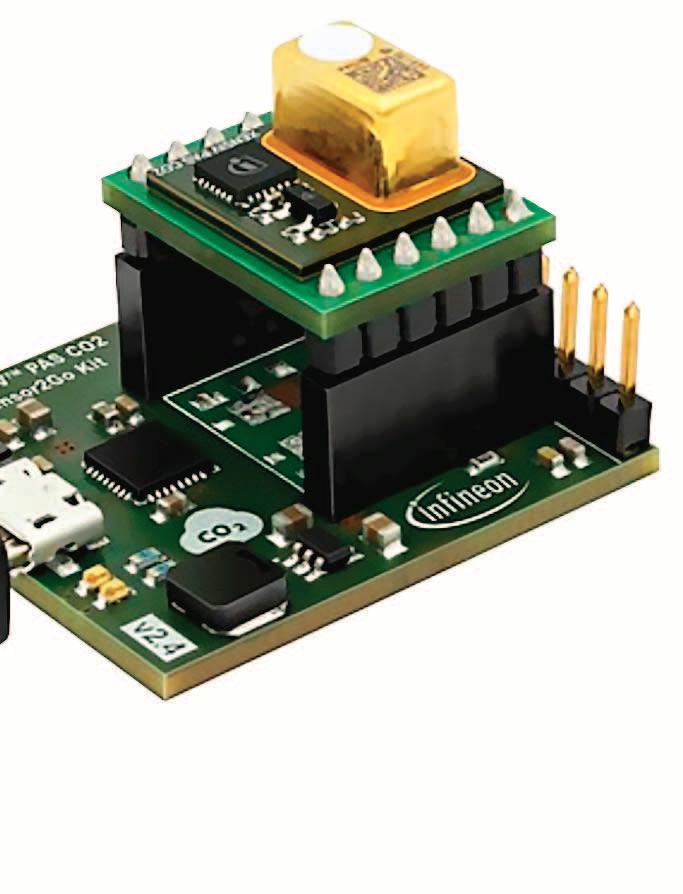
For more information about the XENSIVTM PAS CO2 sensor from Infineon and a direct ordering option, please visit our e-commerce platform at: https://www.rutronik24.com
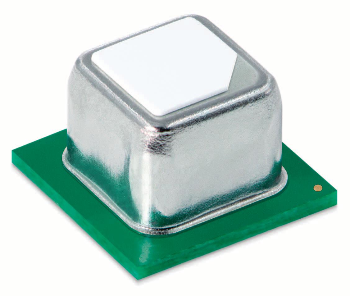
►Rutronik | https://www.rutronik.com
Sensirion, the expert in environmental sensing, has launched a new product in its SCD4x miniaturized CO2 sensor series. The SCD42 has been designed for products that fall under California’s Building Energy Efficiency Standards (Title 24), and is therefore perfectly suited for US HVAC applications. The sensor is now available worldwide through Sensirion’s distribution network.
High levels of carbon dioxide (CO2) compromise humans’ cognitive performance and well-being. Thanks to new energy standards and better insulation, houses have become increasingly energy efficient. However, CO2 produced by human metabolism can accumulate rapidly indoors. Therefore, CO2 is a key indicator for indoor air quality. Measuring indoor CO2 concentration enables smart ventilation systems to regulate ventilation in the most energy-efficient and people-friendly way. Moreover, indoor air quality monitors and other connected devices can help to maintain a low CO2 concentration for a healthy, productive environment.
The SCD42 is Sensirion’s newest addition to the SCD4x product line. Specifically designed for products that fall under California’s Building Energy Efficiency Standards (Title 24), the SCD42 offers unmatched cost effectiveness for the US HVAC market. This disruptive innovation is based on the principle of photoacoustic sensing and combines minimum size with maximum performance to open up numerous new possibilities for integration and application. The SCD42 offers an accuracy of ±75 ppm at 400-1000 ppm. SMD compatibility and its small footprint allow cost-effective and space-saving integration to increase device manufacturer’s freedom of design. This integrated, best-in-class humidity and temperature sensor enables superior on-chip signal compensation and additional RH and T outputs. Finally, the large supply voltage range (2.4-5.5 V) and the robust resistance to external stresses make the SCD42 the perfect fit for all kinds of customer needs.
“Smart building ventilation systems leverage a CO2 sensor to optimize indoor air quality while keeping energy consumption at a minimum. Thanks to its compact size and easy assembly, the SCD42 lowers the hurdle for integrating a CO2 sensor into ventilation systems. I am excited that the SCD42 will help boost people’s wellbeing and reduce our buildings’ carbon footprint,” says Marco Gysel, CO2 Sensors Product Manager at Sensirion.
The SCD42 sensor is available worldwide through Sensirion’s distribution network. Learn more about the SCD42 CO2 sensor at https://www.sensirion.com/scd4x
►Sensirion | https://www.sensirion.com
Miniaturized
for US HVAC applications is now available globally


Cigarette smoke, sweat, sulfur, rancid fat, burned food – the sort of things that nobody likes to have to smell. If you can’t get in some fresh air, then this is where filters become useful. UV-assisted, photocatalytic models are especially effective here. Rutronik’s first deodorizer demonstrator is also based on this technology.
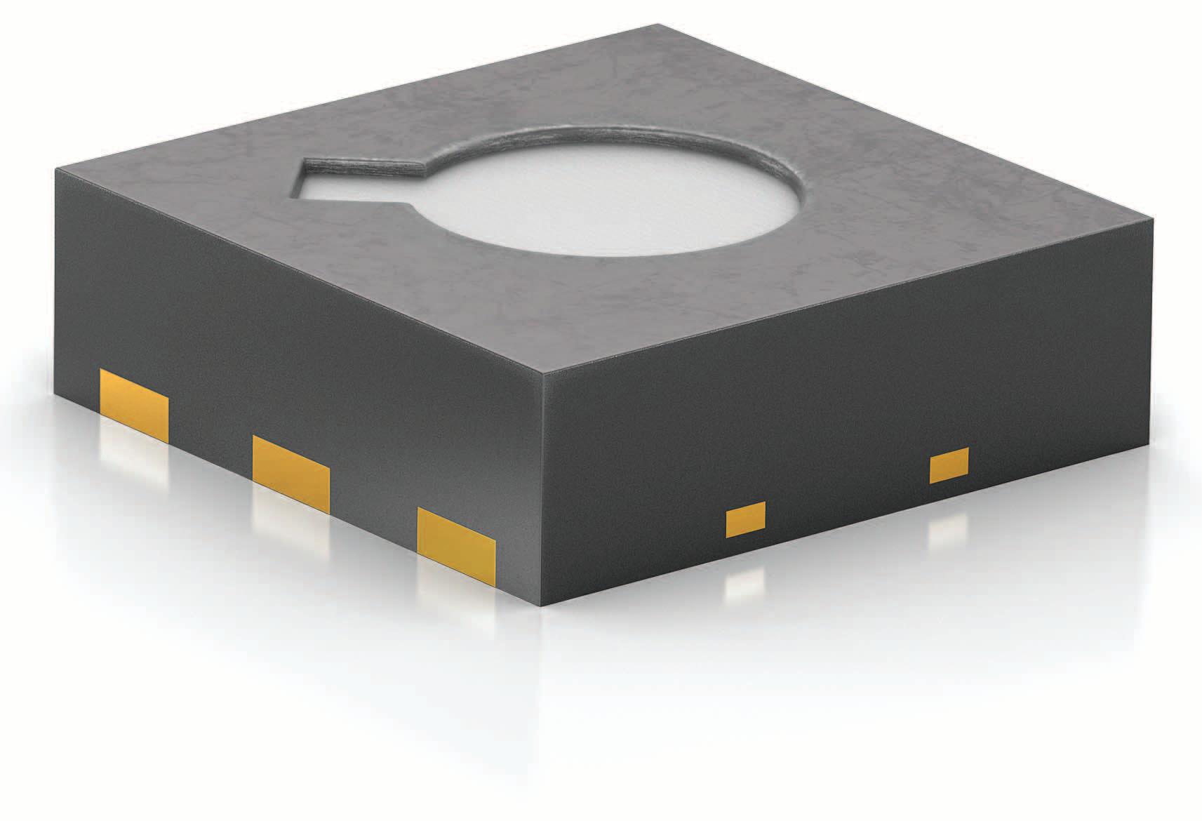
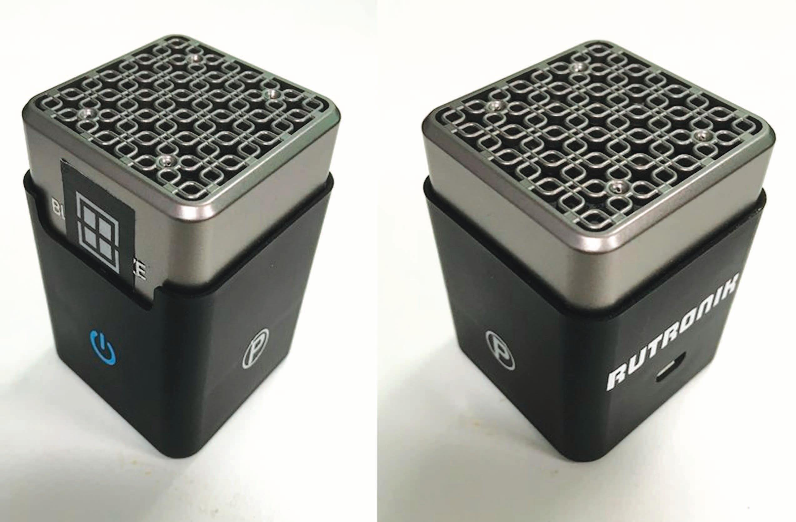
Authors:
Many components of odors are volatile organic compounds (VOCs) such as hydrocarbons (such as methane), alcohols (such as ethanol) and organic acids (such as acetic acid). They are present in many objects, cleaning agents and cosmetics, are secreted by living beings, and are produced in various processes, including the anaerobic decomposition of organic substances (rotting). VOCs can not only create unpleasant odors, but also negatively affect our health, wellbeing and performance. Conversely, air free of such pollutants can be a major boon for our quality of life and health.
Where the concentration of VOCs in the air cannot be reduced by simply increasing the supply of fresh air, effective air purifiers are an important tool. Some of them not only filter unpleasant odors and contaminants but also neutralize gases and destroy pathogens. There are different classes of devices that can be categorized based on how they function: Air scrubbers pass the air through water rollers, causing dust particles to stick to the water film, thus filtering them out of the air. Air purifiers are also known as air humidifiers, as the water molecules are
dispersed into the surrounding air because of the process.
Ionizers generate negatively charged particles that bind to positively charged particles in the air, causing them to increase their mass and drop to the ground. A major disadvantage of ionization is the production of ozone, which is harmful to health in larger quantities. Filter systems pass the air through several filters. Their large surface enables them to adsorb these undesired particles, pathogens and odors. The most wellknown of these right now is the HEPA filter (high-efficiency particulate air filter) and the activated carbon filter (e.g. In water filters). The filter also acts as a reducing agent to absorb ozone or chlorine. Photocatalytic filters use titanium dioxide plates that can be exposed to UV light (UV-assisted titan dioxide photocatalysis, UVTP), producing free radicals that break down organic materials such as VOCs, as well as bacteria and viruses.
UV-assisted TiO2 photocatalysis is already an established feature of water and wastewater treatment, mostly notably for ensuring the quality of drinking water. Their use in air purifiers is less common. They are used in the construction industry and in some urban centers for reducing the toxic pollutant content of the air. The latest findings indicate that UVTP can also guarantee the microbiological safety of foods.
Two studies from the Kanagawa Institute of Industrial Science and Technology (KISTEC) in Japan recently demonstrated using a UVTP-based deodorizer how this method of photocatalysis is extremely effective against odors. The results were confirmed by the Japan Food Research Laboratories. These studies involved acetaldehyde, a gas with a pungent odor, being pumped into a 36-liter tank until a concentration of 10ppm was achieved.
The deodorizer was then activated and the concentration was measured over a period of 60 minutes using a photoacoustic multi-gas monitor. The result: After 14 minutes, the share of acetaldehyde was just 0.1ppm, after 23 minutes it was just 0.05ppm. The process was repeated several times, in each case following the same procedure. For a comparison, the institute used an ionizer with the same test construction. This reduced the acetaldehyde concentration by just 40% within an hour. Without any air purification measures, 95% of the acetaldehyde was still present after an hour.
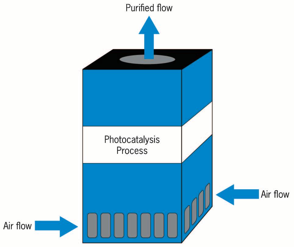
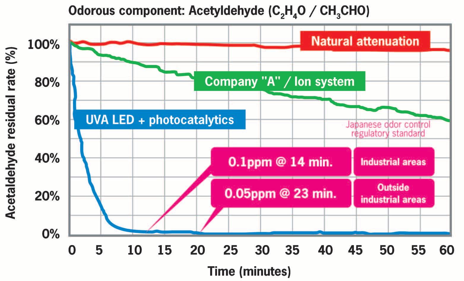
The UVA-LED NDU1104ESE-365 from Stanley with a wavelength of 365nm proved to be the most effective model for the UV source in the studies. UVALEDs with wavelengths of 385nm or 395nm neutralized much fewer VOCs. Its drive current of 500mA also makes the NDU1104ESE-365 more effective than other models with lower values, because light output rises with current.
Deodorizers from Rutronik


Based on these findings, Rutronik has developed a deodorizer demonstrator. At the base of its quadratic housing (48mm ×
presence of oxygen, with the doped O2 atoms of the metal oxide (MOx) bonding with the odor molecules. The electrons that this reaction releases cause a change in the electrical resistance of a film made of metal oxide nanoparticles. This is how the sensor detects a wide variety of VOCs and other gases playing a fundamental role in odors and the quality of a space’s air.
The same tests produced almost exactly the same results with ammonia (smell of urine), methyl mercaptan (smell of feces) and formaldehyde (smell of pungent cleaning agents). Only in the test series for hydrogen sulfide (rotting and sulfur odor) and trimethylamine (unpleasant fish smell) did the deodorizer need to be used for longer to achieve a comparable result. After two hours, almost all of these VOCs were also barely measurable.
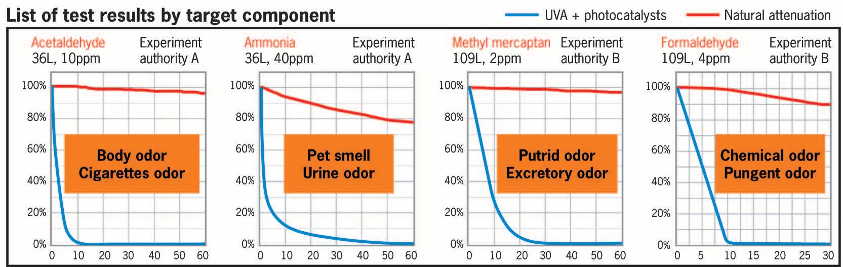
48mm × 60mm), air flows into the device. A fan ensures that the air moves up from the bottom through the housing, passing through a photocatalytic filter located between two UVA-LEDs with a wavelength of 365nm and a drive current of 500mA.
Rutronik used the SGP MOX sensor from Sensirion to determine the VOC content. It is mounted next to the LED and is based on the “chemisorption” of gases in the
If the number of VOCs exceeds a certain value, the LED is activated. The radiation time is based on the type and quantity of the VOCs. Optionally the values measured by the sensor can also be displayed so that users can always read the air quality values. The rechargeable lithium-ion battery with a charge life of two hours can be charged at any household mains socket, on a PC or using a car charger, making it portable and flexible. This allows businesses to test its effect anywhere, be it in public or portable toilets, trash rooms, industrial kitchens or fitness studios.
The Rutronik deodorizer is still in the test phase – but should it prove to be suitable in practical use, it would be an important step in fighting unpleasant and harmful odors. Moreover, that is when air fresheners, paper air fresheners and room sprays will cease to have any purpose.
►Rutronik https://www.rutronik.com

Five Higher Technical Schools (Höhere Technische Lehranstalten, HTLs) in Carinthia and six in Tyrol received highprecision CO2 sensors from Infineon Technologies Austria AG and MCI in Innsbruck. The teams of students will use them to build CO2 alarm lights to indicate the necessity for ventilation thus reducing the risk of infection. A total of 300 classrooms will be equipped.
Indoor CO2 levels are an important indicator of air quality. Particularly in the current pandemic, this value can help contain the spread of viruses. Regular crossventilation and shock-ventilation of classrooms – in addition to ongoing testing and mask-wearing – is therefore also included in the specifications of the Austrian Ministry of Education. But when is it time to ventilate? To clarify this question, Infineon and the MCI are providing
the CO2 sensor kits free of charge to eleven technical teaching institutions in Carinthia and Tyrol in order to use stateof-the-art technology to draw attention to the need for timely ventilation in the classroom.
In the spirit of “learning by doing”, the young technical talents use Infineon’s sensors to build their own air quality measurement systems that warn of excessive CO2 concentrations and thus reduce the risk of virus transmission. Learning in a healthy indoor environment is of paramount importance, especially in times like these.
“With our initiative we want to support the young talents in their technology educa-
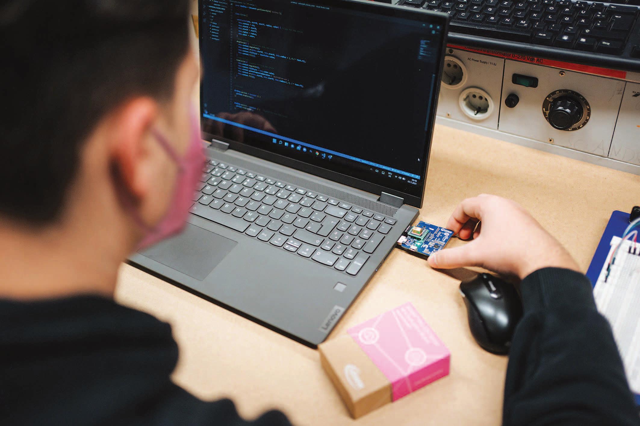
tion and enable a healthy learning atmosphere in the classroom,” said Sabine Herlitschka, CEO Infineon Austria. “The students as well as the teachers are actively involved, they can combine the knowledge of several subjects – from electronics, computer science to physics – and link this to health-related topics. This encourages participation, strengthens team spirit and creates digital solutions with a benefit for the entire school.”
At the heart of the CO2 sensor is an Infineon module based on XENSIV PAS technology. It measures the CO2 content precisely, reliably and continuously. In addition, other parameters such as temperature, humidity and air pressure are measured. As soon as a threshold value is
exceeded, an alarm can be triggered via a CO2 alarm light. According to the Austrian Ministry of the Environment, the CO2 concentration in classrooms should not exceed an average of 1,000 ppm (parts per million, i.e. 0.1 percent by volume). Since the concentration of aerosols through which the virus is transmitted correlates with the concentration of CO2, the CO2 sensor can help ensure that people can meet in safe indoor-conditions – whether in the office, at school or at home.
“We have created an easy-to-use system solution in our innovation lab, the ‘Emerging Applications Lab’, which is run jointly with Infineon, and it is already in use in twelve lecture halls in Innsbruck,” said MCI Rector Andreas Altmann. “Another 50 lecture hall systems are in preparation. With the display of the CO2 value, we have an objective benchmark for the energy-efficient supply of fresh air, can ventilate according to demand and avoid unnecessary energy losses, especially during the winter season. We are happy to pass on this developer and user know-how to the schools.”
At school, the students learn to build and program a CO2 alarm light under the guidance of the teachers. This allows them to deepen their hardware and software knowledge, create a digital design with LEDs and acoustic signals, control the system and expand it to an Internetof-Things platform. To this end, a dedicated developer forum was set up across the schools to network, share knowledge and develop ideas for further innovations. Digital technologies thus offer real added value for education and collaboration.
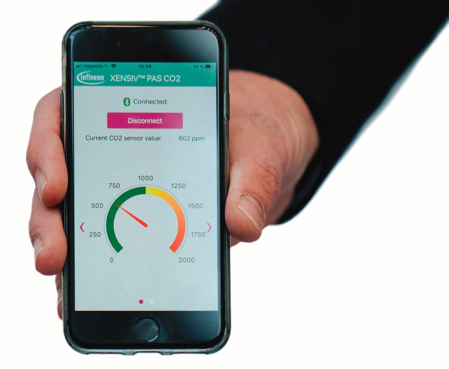
The school team at HTL Villach is going one step further: the CO2 sensors are not only being used in the classes, but are also to be integrated into the technology of the building refurbishment currently underway. Combining them with the infrastructure control concept will
enable automated and continuous data collection and data evaluation for the entire school. For example, noise levels could also be measured in the future. This practical collaboration between industry and education shows how STEM subjects (Science, Technology, Engineering, and Mathematics) can be used to create smart solutions for topics at the cutting edge of technology. Thus, it is an active contribution to practice-oriented education, as well as to qualified technical specialists in the region.
About
MCI | The Entrepreneurial School ® combines elements and features of universities, business schools, grande écoles, universities of applied sciences, business and consulting. With its unique concept, it stands for science, studies and advanced education, for internationality, quality, innovation, practice orientation, cooperation with business and industry, solutionoriented research and development, top infrastructure, customer and service orientation and international renown.
Since 2016, Infineon has been operating the “Emerging Applications Lab” in cooperation with MCI. In this innovation lab, Infineon sensors are used to develop socalled system demonstrators, which are used, for example, for motor controls in collaborative robotics or high-frequency power electronics with gallium nitride semiconductors. For more information please refer to www.mci.edu
Infineon Technologies
https://www.infineon.com
Intelligent solutions: modern code readers identify the part type – laser scanners and light barriers safeguard the work area.
Industrial robots are often used for automated loading and unloading of machine tools. In so-called robot cells, numerous swivel and gripping movements are performed in a very short period of time.
These zones must be reliably protected against access over a large area. Before the robot picks up a part, the part must be uniquely identified to ensure that the correct processing step is carried out.
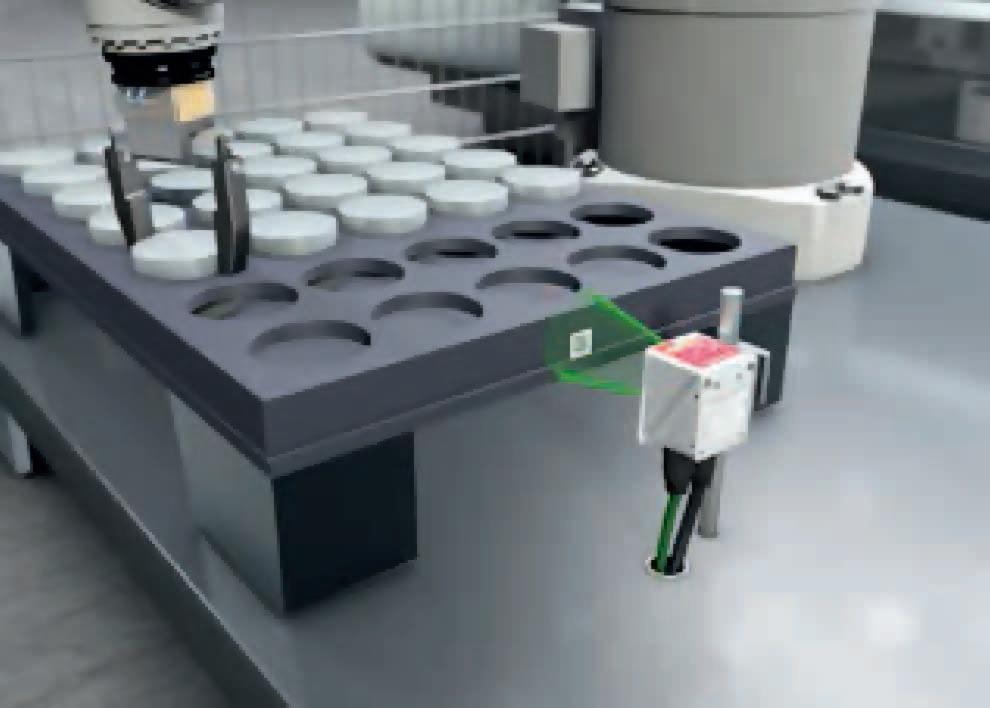
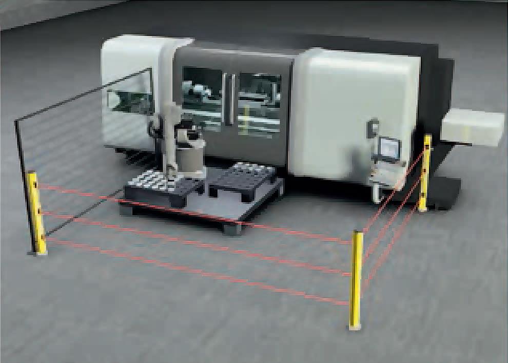
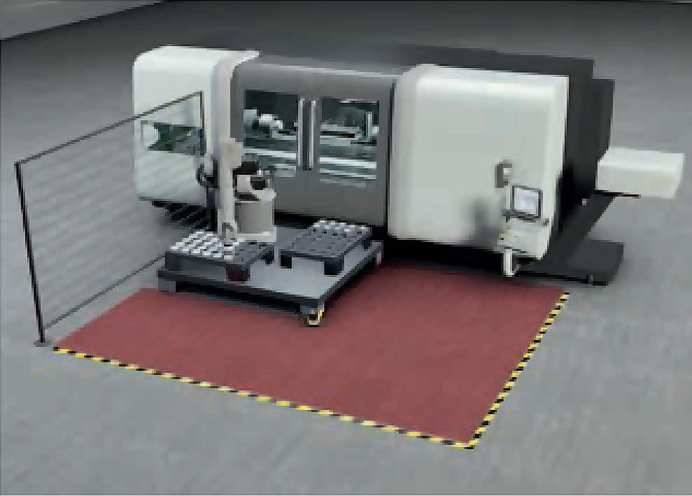
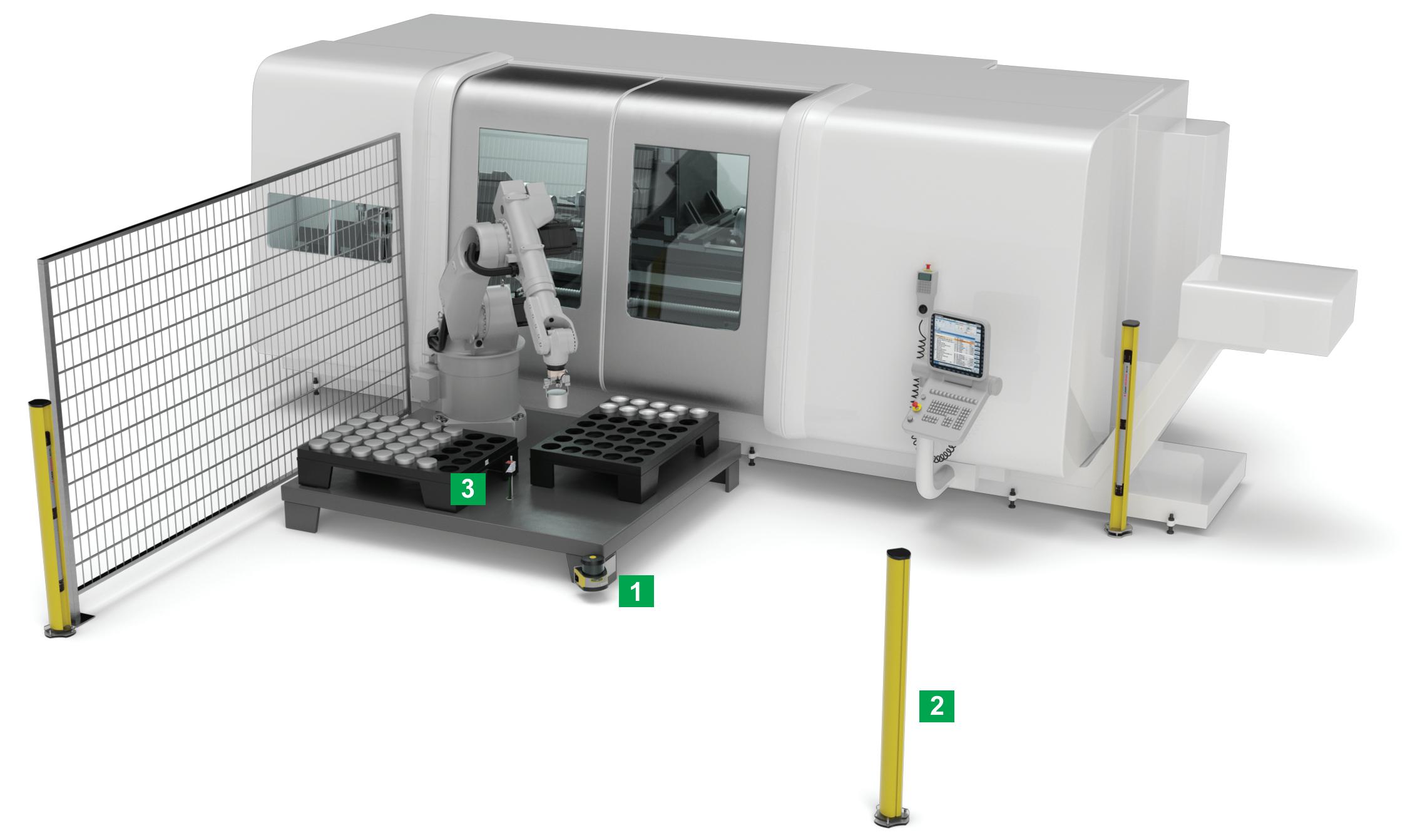
Our safety laser scanners reliably monitor large danger zones around robot cells. Modern code readers are easy to configure and are characterized by a high reading performance. This ensures that the correct work piece is passed on to the next work step.
Area protection
–Monitoring of the front and side machine areas with just one device with 270° scanning angle
–Staggered operating ranges from 3 – 8.25 m
–Two autonomous protective functions
–Fast alignment in just 5 steps using configuration software
–Simple installation through integrated level and removable, intelligent connection unit with configuration memory
Access guarding 2
–Transmitter / receiver system with a range of up to 70 m, even around corners with multiple mirror columns
–Transceiver system with operating range up to 8 m
–Integrated laser alignment aid for time-saving and economic alignment
–Simple configuration by means of wiring
–Device exchange by means of Plug & Play via M12 connection technology

–Integrated indicator light for status display, even over long distances
–Optional AS-i interface


–Identification of 1D- and 2D-codes
Identification 3 www.oboyle.ro
–Models with reading distances from 40 – 360 mm
–Integrated interfaces, such as Ethernet, RS232 / 422, PROFINET
–Browser-based, multi-language WebConfig tool for access via Ethernet as well as configuration and diagnosis
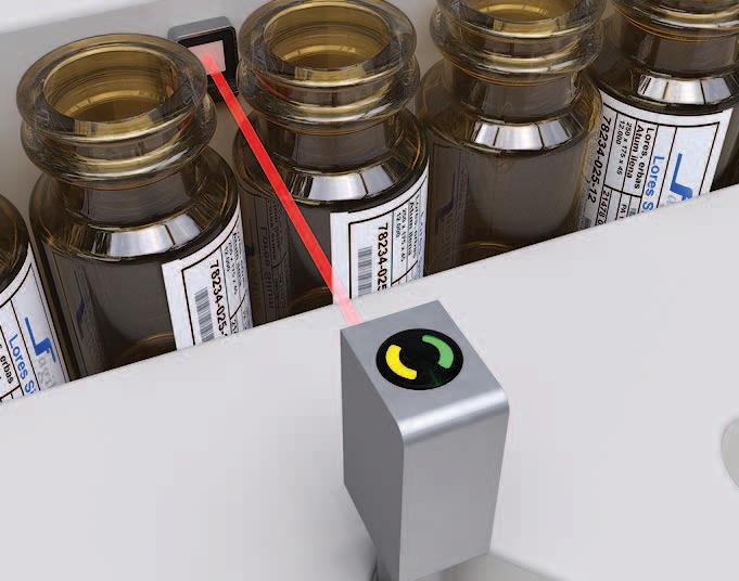
Always safe, always reliable: Extremely reliable stainless-steel sensors meet the highest safety and hygiene standards.
The packaging process mainly involves tablets being packed in blisters and various liquids being filled into small glass and plastic bottles. Owing to the strict hygiene standards, stainless steel is often the only material allowed for the components used. Maximum safety requirements apply during the production and packaging of pharmaceutical products. To protect against falsification, code readers must guarantee 100% decoding. The DCR 200i bar code scanner reads all codes and ensures the traceability of the production and packaging process for all products. With its hygienic stainless-steel housing, it is ideally suited to the demands of the pharmaceutical industry. The hygiene design stainless steel sensors of the 53 series use laser technology to reliably and quickly detect even minute vials. Many challenges involving the detection of self-adhesive labels in the labelling station can also be mastered: For example, the GSU 14D forked sensor can reliably detect virtually invisible clear-on-clear labels. In quality control, the LRT 8 luminescence sensor also reliably checks the presence of attached paper labels.
Precise positioning of vials
Detection of vials in screw conveyor

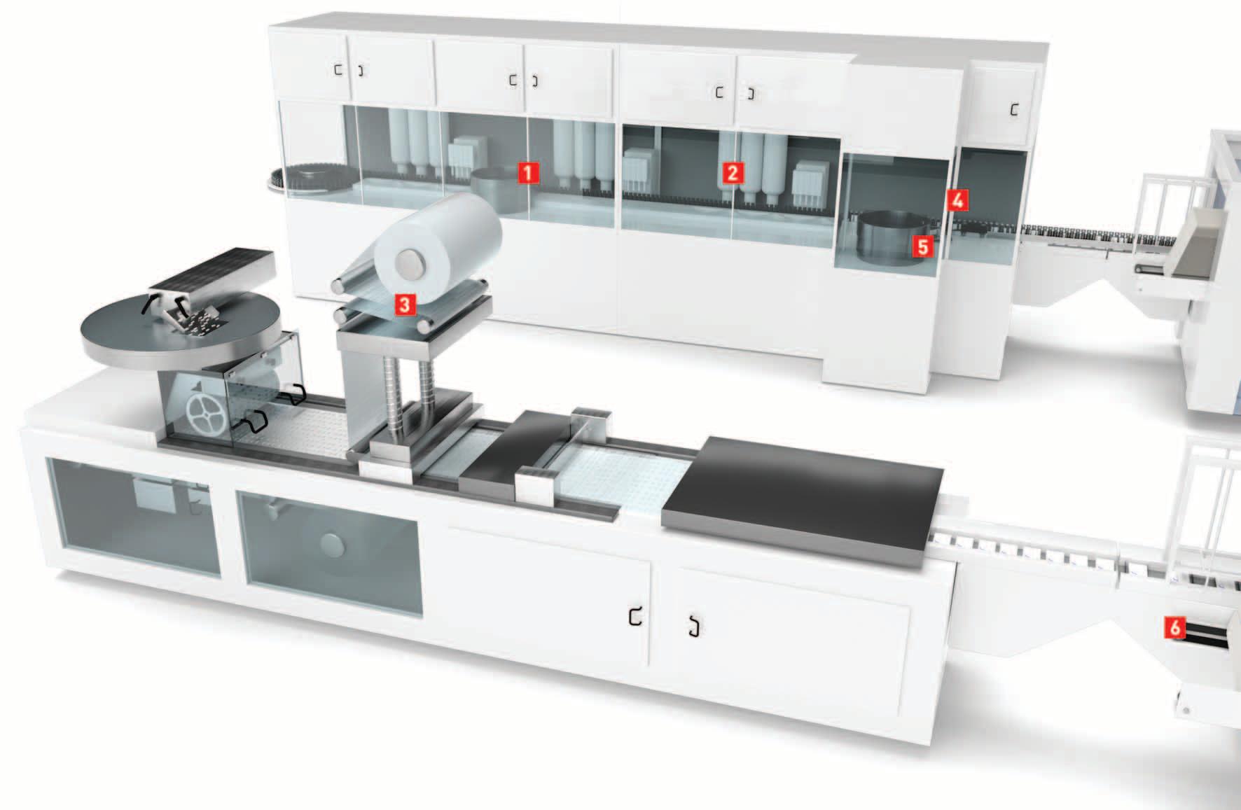
■ Hygienic design of laser retroreflective photoelectric sensor and reflectors
■ Integration also in confined spaces
■ Highly precise positioning thanks to the small laser light spot
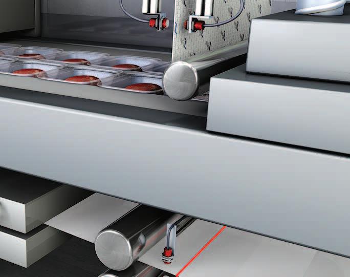
■ Chemical resistance tested in accordance with ECOLAB
■ Extended cleaning agent long-term test (CleanProof+)
■ Precise background suppression through special V-optics
■ Reliable detection of transparent objects in front of a moving background
■ Simple mounting with integrated metal threaded sleeve
■ Robust plastic housing with degrees of protection IP 67 and IP 69K
■ Multicolor contrast sensors with high precision and reliable switching behaviour
■ Easy teaching of the marks via various teach modes or potentiometer
■ Convenient adjustment via dual-channel IO-Link interface
■ Tracking function for compensating contamination
■ Degrees of protection IP 67 and IP 69K and ECOLAB certification
■ Clearly visible light spot allows easy alignment and fast commissioning
■ Reliable detection of all types of containers
■ Tracking function for fault-free continuous operation
■ Simple sensitivity adjustment via teach button
■ Plastic or stainless steel housing with degree of protection IP 67 and IP 69K
■ Broad product portfolio for detecting a wide range of label materials – from paper to transparent film
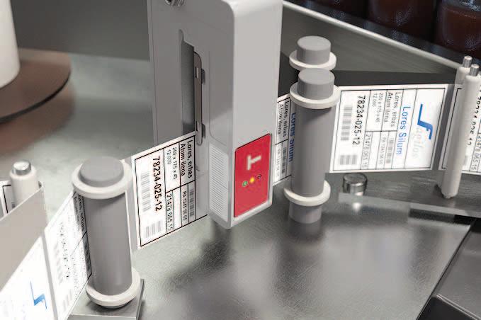
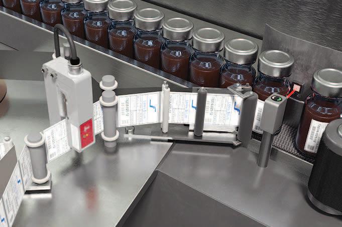
■ Maximum dispenser accuracy
■ Conveyor speeds > 2 m/s
■ Simple sensitivity adjustment via teach button or potentiometer
■ Multiple parameter sets can be stored
www.oboyle.ro
POSITAL’s updated analog programmable rotary encoder are now available with even more features.
■ Broader supply voltage range for mobile machine applications
■ Increased accuracy, resolution and number of turns
■ Further programmability function with our UBIFAST configuration tool

■ Singleturn encoders with measuring range less than 360 degrees available
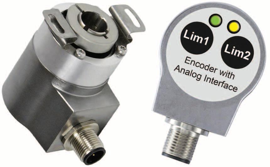
POSITAL has launched the new generation of analog rotary encoders for position control. Compared to the earlier analog encoders, these new models feature improved accuracy, faster dynamic response and new programming options. They also accept a wider range of supply voltages, an advantage for mobile machinery applications.
POSITAL’s analog encoders are designed for positioning tasks that use analog control systems. Outputs are either voltage (0-5V, 0.5-4.5V, 0-10V or 0.5-9.5V) or current (420mA). The magnetic measurement mechanism is wearfree and extremely durable so that these devices offer much better accuracy, reliability and service life than conventional potentiometers.
■ Fast and reliable identification of 1D- and 2D-codes
■ 3 optics models cover reading distances from approx. 40 – 360 mm
■ High reading performance and powerful LED illumination enable reliable use even with low print quality and poor contrast in the code
■ Easy commissioning at the device or using the install wizard in the web browser
■ Degree of protection IP 67 and IP 69K (stainless steel housing)
An important feature of the POSITAL analog encoders is that they are programmable with measurement characteristics that can be customized to meet specific application requirements, (it is also available with POSITAL’s digital encoders with SSI and incremental interfaces). Programming can be carried out at the factory, in a distributor’s warehouse or at the customer’s job site, thanks to POSITAL’s easy-to-use UBIFAST programming tool. Programmable characteristics include direction of rotation (CW or CCW), zero set and the encoder output range. Measurement range programming allows the full range of electrical outputs (voltage or current) to be set to match a user-defined range of mechanical motion, resulting in significant improvements to control system accuracy. For single-turn models, the measurement range can be set to 90°, 180°, 270° or 360°. For multi-turn models, the range can be set anywhere between 1 and 65,536 complete rotations. Analog encoders are available with push-buttons on the housing that enable the user to easily specify the upper and lower limits of the mechanical motion, with the electrical output fully spanning this range. www.oboyle.ro
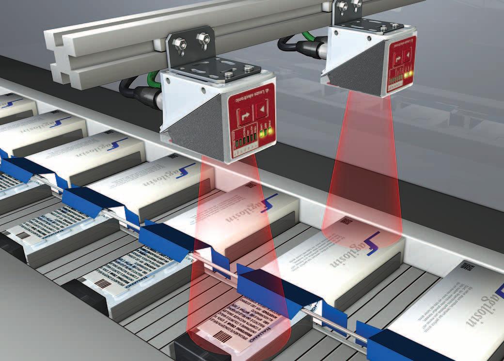
With the diffuse reflection sensors of the 3C, 25C, 46C and 49C series, active ambient light suppression was enhanced and the functional reliability thereby greatly increased. The sensors can even withstand direct light from LED hall lighting without causing any erroneous switching.
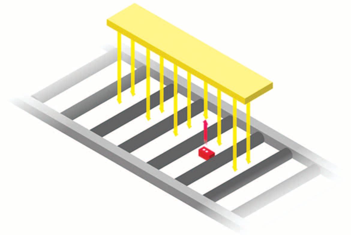
In production and mounting areas, sensors for object detection are often mounted between the rollers of conveyor belts due to space limitations. It is not possible to install a receiver or reflector in this case. This is why diffuse reflection sensors with background suppression are used. The ceiling lighting has pulsed light. The pulses are not visible to the human eye. When the optics of the installed sensors face the hall ceiling directly, faulty switching may occur when the pulsed light beams collide with the pulsed light beam of the sensor.
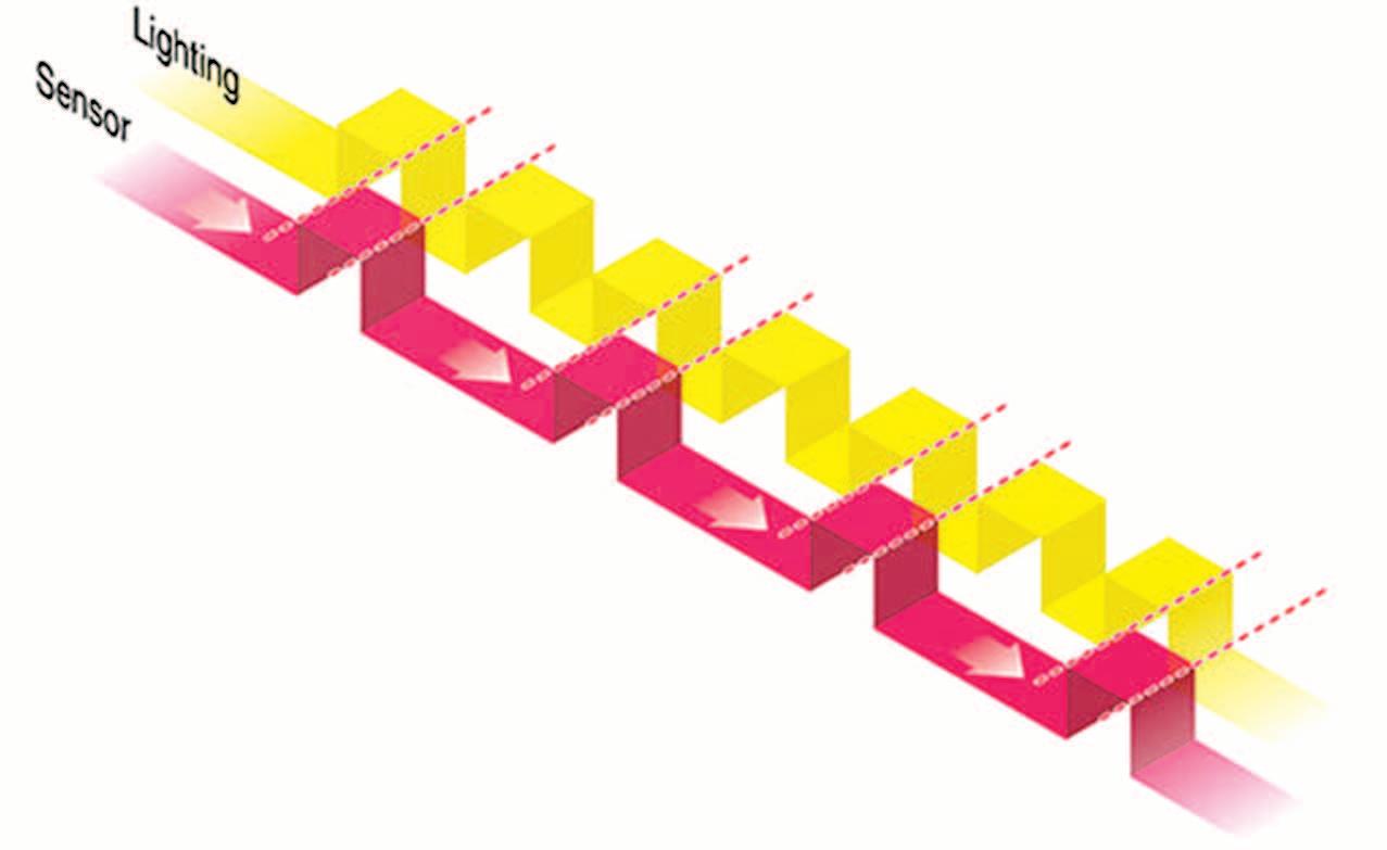
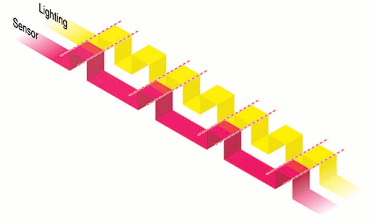
The solution: diffuse reflection sensor with active ambient light suppression (A2LS)

Our diffuse reflection sensors have been featuring active ambient light suppression for many years. This function allows the senor to distinguish between ambient light and the light that is reflected by the object. When ambient light is detected, the sent pulses are timeshifted to prevent them from colliding with the pulses of the ceiling light.
Modern LED illumination is increasingly used in production halls for efficiency reasons. In these cases, the light is pulsed significantly faster compared with traditional ceiling lighting, such as neon lights. The previously used process for ambient light suppression is unable to deal with these types of lighting situations.
To meet the new requirements, we have significantly optimized ambient light suppression in the diffuse reflection sensors of the 3C, 25C, 46C and 49C series. These series feature integrated ASIC-based electronics platforms with a high interval and optional, parallel signal processing. This makes it possible to very quickly analyze high-frequency pulsed ambient light and the sensor's reaction to it. The sensor holds off on sending the pulse so that it is sent while the LED light is not pulsing.
Our HF variants are ready today to handle the requirements of the future
We expect that the current trends towards increasing pulse frequency in LED illumination will continue. For this reason, we have already developed variants that can withstand direct, intensive light exposure and whose ambient light suppression is designed for a particularly high pulse frequency (HF).

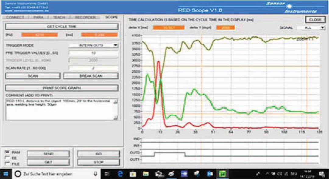
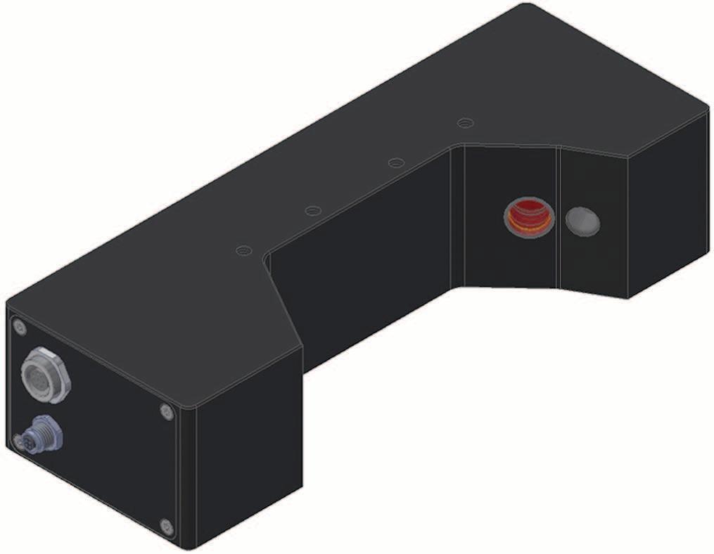
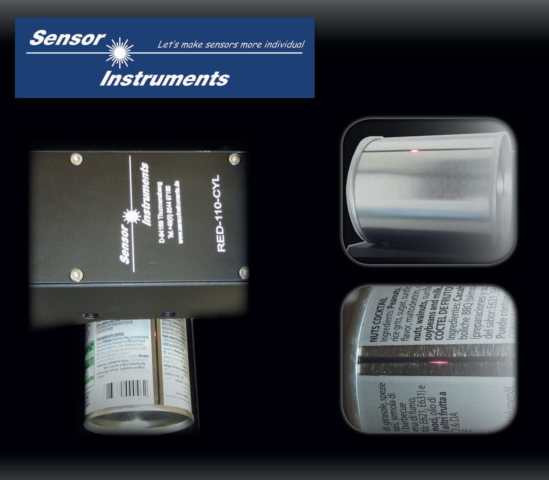
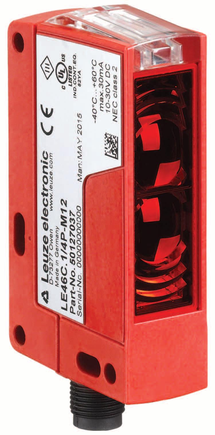
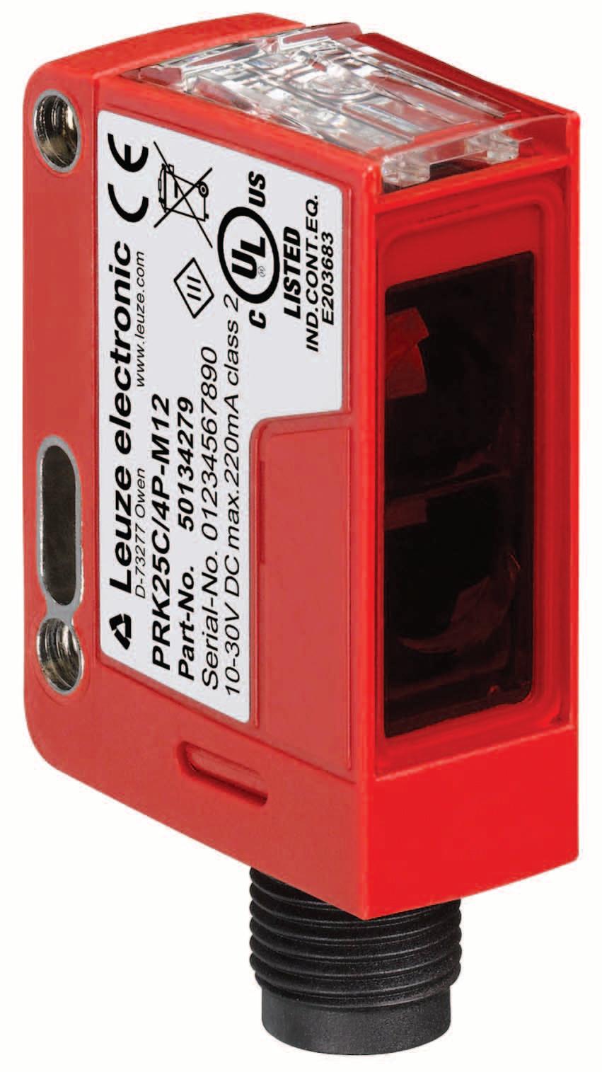
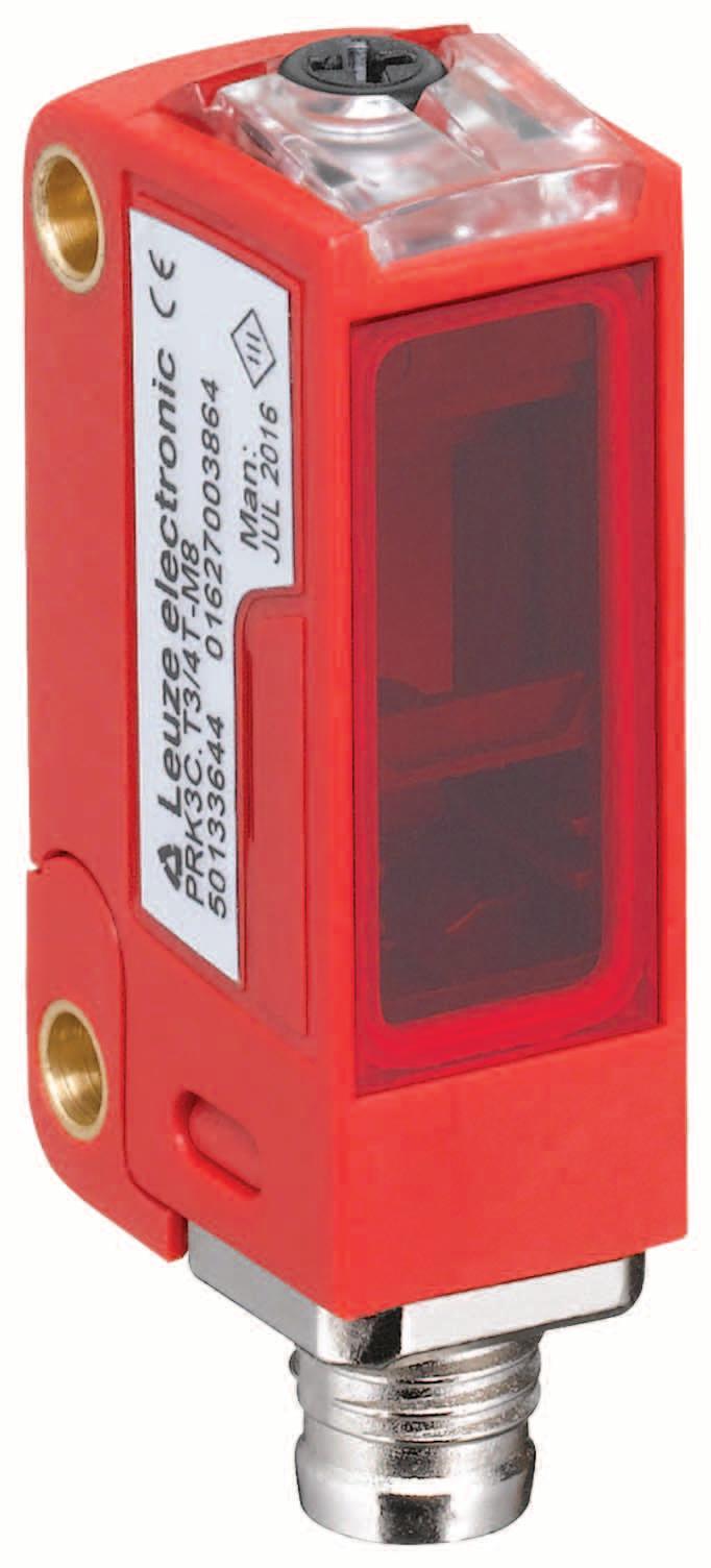
For the detection of welding seams, contrast or color sensors would seem to be the proper solution, because in most cases the welding seam optically shows a clear difference from the surrounding product surface. In everyday practice, however, it turns out that these methods involve frequent readjustment and reparameterization. On the one hand this is due to the varying, product-dependent distance of the object surface from the sensor, and on the other hand to the highly alternating appearance of the respective welding seam with respect to color and contrast. Both methods, however, seem to be completely unsuited for printed objects, especially if a color or contrast similar to the welding seam is already contained in the printed material. So-called eddy current sensors offer a completely different approach, because the metallurgical structure of the object in the welding seam differs from the remaining metal sheet. This method, however, requires recalibration of the measuring equipment when the product changes with respect to sheet thickness, metal type, welding method, and distance of the object from the sensor. Edge detectors might offer an alternative here. All that is required is the existence of an edge, which by nature should be the case with a welding seam (with the exception of polished welding seams). The sensors of the RED series operate with the principle of edge detection. A laser spot or a focused laser line is projected onto the object surface. The laser spot is detected by two photodetectors that are integrated in the laser sensor. These two detectors are positioned in such a way that the detector that is close to the laser transmitter receives more light when there is an edge, whereas for the detector that is opposite to the laser transmitter the laser light beam so to speak is blocked. The sensor's integrated controller with its software then compares the signals of the two detectors and provides a result that is independent of the intensity. The outstanding feature here is that smallest edges, even on printed objects, are reliably detected by the sensor (RED-110-L) in a distance range from 90mm to 130mm. The advantages of edge detection! www.oboyle.ro
In the production of oil and air filters for the automobile industry these filters must reach the required throughput rate, which is achieved by folding the filter material so that it provides a large filter surface on a minimum of space. Depending on the filter type there are differences in the fold depth and in the numbers of folds. Before the filter mats are formed into a cylinder they are transported on a linear table as endless material. When the required number of folds is reached, the filter mat is cut off from the endless material. During feeding the individual folds are alternately contracted and extended, and the folds are counted by means of a non-contacting method. The differing fold height, detection in contracted condition, and the filter material itself due to its semi-transparent properties, are challenging factors for the sensor system.
Accurate edge counting under these conditions can be performed with the edge detectors of the RED series. The focused laser line that is projected onto the folds is picked up by means of two photodetectors under two different angles. While one detector is arranged near the laser transmitter, the second receiver is placed on the sensor side that faces away from the transmitter. When there is a fold, the laser spot is blocked for the detector facing away from the transmitter, whereas the signal of the receiver that is near the transmitter rather is amplified. The relationship of the two received signals provides reliable information about the existence of a fold. Additional software algorithms such as for example the activation of a dynamic dead time after fold detection and a switching hysteresis further increase the counting accuracy. With the RED-110-L there now is a sensor that reliably detects folds within a distance of 90mm to 130mm from the object. It does not matter whether the folds are in contracted or extended form. The maximum scan frequency of the laser sensor typically is 100 kHz and should thus be more than sufficient for this application. https://www.oboyle.ro
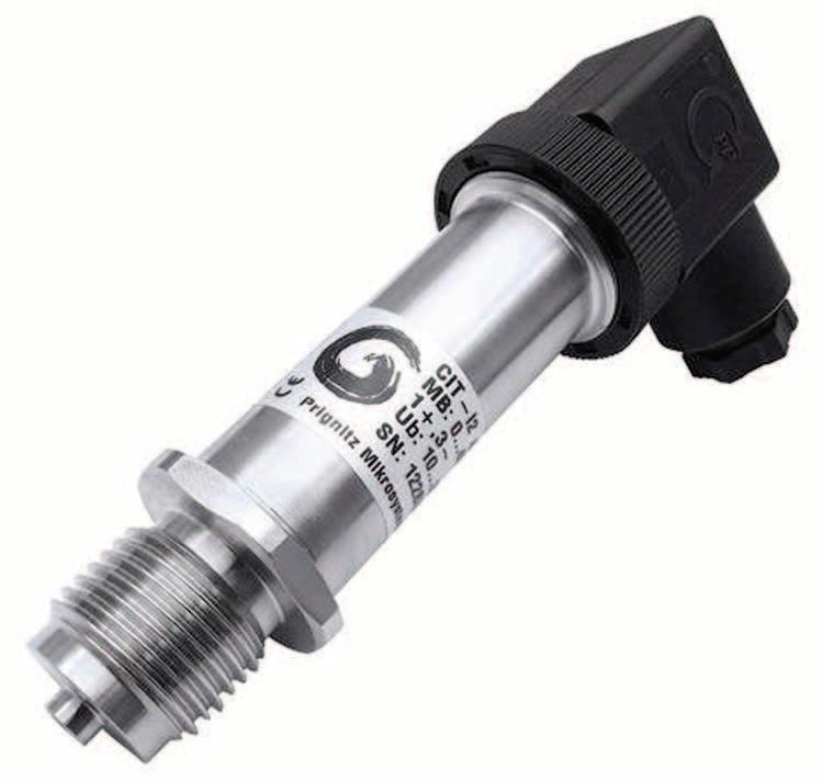
The piezoresistive semiconductor measuring cell of the industrial pressure transmitter SPT-Ti is made of titanium and based on a silicon on sapphire technology making it absolutely vaccum tight. Leakage of internal sealings due to material fatigue is ruled out right from the start. It does not contain any disturbing pressure transfer fluids and no large pressurized surfaces. Connection to the connecting pins is made by gold bonding making it absolutely sturdy even in case of low temperatures, shocks or vibrations. Signal processing of the measurement bridge is effected by a mixed-signal ASIC. Titanium offers a whole range of benefits. The sturdy oxide layer provides high corrosion resistance. Moreover, titanium has got an enormous strength at a relatively low density and can be used for pressure ranges up to 5,000 bar in the long term. Thanks to the oustanding thermal characteristics and resistance of titanium the SPT-Ti can be used in high-temperature applications with medium temperatures up to 200°C.
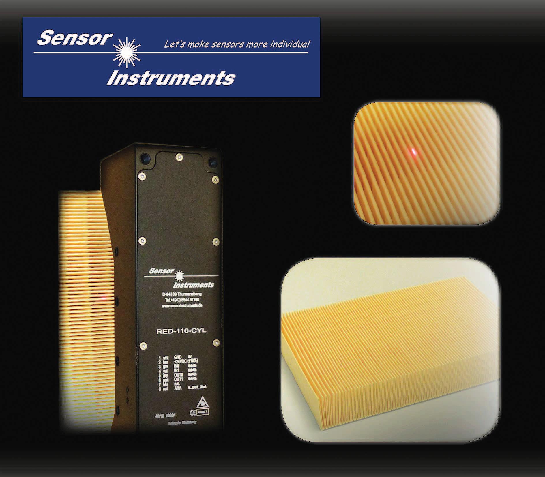
• 2.5 bar up to 5000 bar
• Relative pressure, absolute pressure, sealed reference
• (0) 4 ... 20 mA, 0 ... (5)10 V, radiometric and more
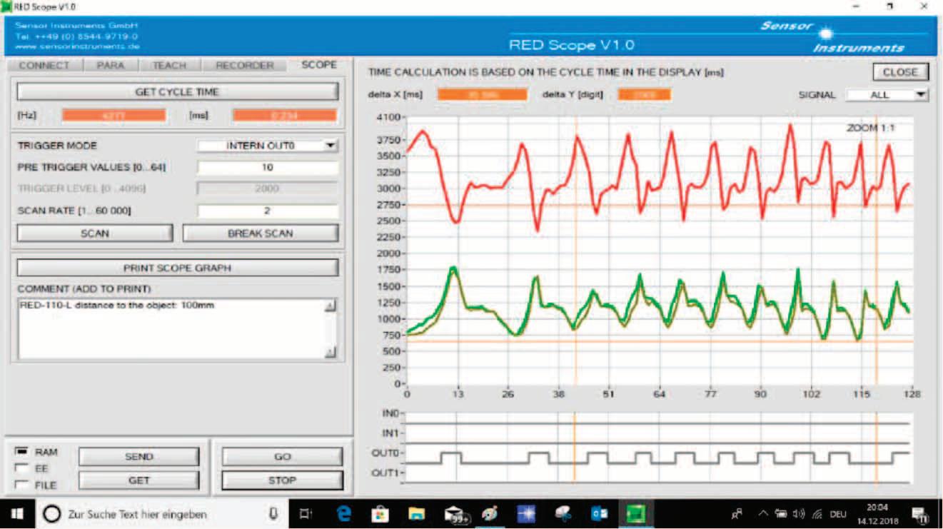
• ISO 4400, M12x1, cable and a lot more
• medium-contacted parts made of titanium
• Precision < 0.5 % FS (setting of limit value)
• Response time < 1 ms
• Medium temperature up to 200°C
https://www.oboyle.ro
■ no seal required
■ extremely robust
■ long-term stability
■ high chemical resistance
■ insensitive to overload conditions