


4/2022
PAN EUROPEAN MAGAZINE https://international.electronica-azi.ro INTERNATIONAL
A


Mouser Electronics, Inc., the New Product Introduction (NPI) leader™ empowering innovation, supplies purchasing professionals and engineers with the resources and new products they need to embark on the next frontier of automotive solutions. Through blog posts, articles, videos, and more, Mouser and its leading manufacturer partners provide a deeper understanding of modern automotive challenges and solutions, providing insight into the future of the automotive industry. Highlights include a look at how driver monitoring systems use AI and sensor fusion to improve vehicle safety and an exploration of 5G vehicle-to-vehicle (V2V) and vehicle-to-infrastructure (V2I) networks in enhancing fleet telematics
Mouser stocks the industry’s widest selection of semiconductors and electronic components™, including the following solutions ideal for automotive applications:
• Toshiba SSMx automotive N-channel and P-channel MOSFETs offer a range of features that cover automotive applications in 12 V to 48 V battery systems. The wafer processes and low-resistance technology work together to suppress switching noise and reduce energy loss.
• The Microchip Technology LX34070 inductive position sensor is designed specifically for electric vehicle (EV) motor control applications.
The IC’s differential outputs and high sample rates make it ready for the Safety Element out of Context (SEooC) defined by ISO 26262.

• TE Connectivity multi-band GNSS ceramic antennas enable improved location information to centimeter accuracy for applications such as fleet telematics, vehicle tracking, drones, and smart transportation.
For the latest automotive design resources from Mouser, visit https://resources.mouser.com/automotive Mouser Electronics https://www.mouser.com


Analog Devices, Inc. (Nasdaq: ADI) invites the public and media to experience life at the Intelligent Edge through interactive demonstrations and expert discussions at CES 2023.
Visit the ADI booth: Connecting the physical and digital worlds by both sensing and processing at the edge will make data and insights available where decisions are made, resulting in faster and more effective execution. Stop by booth #4725 at the Las Vegas Convention Center West Hall to learn how the Intelligent Edge will impact every moment of our lives, big or small, to solve some of the world’s greatest challenges by enabling a more efficient, safer, and sustainable future.
“Insights from the Edge” Panel Sessions: ADI executives will be joined by experts and thought leaders in a series of conversations about how technology is enriching lives and accelerating human breakthroughs. All discussions will be held at ADI’s booth. For any updates on panel sessions or details regarding ADI at CES, please visit www.analog.com/ces.
Panel sessions:
• The Future of Automotive: Bringing Personalized and Immersive Experiences into the Vehicle
- Thursday, January 5, 11:30-11:55 a.m.
- Participants: ADI, Jaguar Land Rover, and Harman
• The Ocean’s Critical Role in Combatting Climate Change
- Friday, January 6, 12:00-12:25 p.m.
- Participants: ADI and Woods Hole Oceanographic Institution (WHOI)
Demonstrations: Explore 30 live demos featuring ADI’s technology to see how the Intelligent Edge will continue to advance the efficiency, safety, and sustainability in our daily lives from the ordinary to the extraordinary.
• Automotive: Explore how ADI’s innovations are enabling a more personalized, immersive, safe, and sustainable mobility experience. ADI’s advancements in connectivity, audio processing platforms, and power management solutions are pioneering a seamless transition from home to vehicle.
• Consumer: Discover how ADI’s technology is making the office work from anywhere, as well as streamlining and enhancing the way we create and enjoy movies, music, and media.
• Digital Healthcare: See how ADI’s sensing technologies in a range of wearables continuously monitor body vital signs to support the management of health and sleep patterns.
• Industrial: Watch how terrain-based navigation and stabilization is helping to make workdays safer and more productive. See ADI’s technology in action as it helps vehicles operate more safely and efficiently in agriculture, on construction sites, and more.
Award-winning tech: Learn more about the ADTF3175 which earned a 2023 CES Innovation Award for opening up endless possibilities in augmented and mixed reality.
The ADTF3175 is the industry’s first highresolution, industry quality, indirect Timeof-Flight module for 3D depth sensing and vision systems. The CES Innovation Awards are based upon descriptive materials submitted to the judges.
Analog Devices https://www.analog.com
Siemens Digital Industries Software today announced that its Sokol™ Flex OS software now supports RISC-V embedded development with the availability of one of the industry’s first commercially supported, extensible, and customizable Linux® platforms for the RISC-V architecture. Based on the popular, open-source Yocto Project industry standard, Siemens‘ Sokol Flex OS helps embedded developers create customized, Linuxbased systems for RISC-V architectures with ease, security and confidence.
The RISC-V architecture is ideally suited for industrial, medical, defense-aerospace, and consumer applications. Semico Research predicts that global deployment of the architecture will reach 62.4 billion cores by 2025.
Siemens’ Sokol Flex OS for the RISC-V architecture streamlines application development, allowing customers to focus on value-add differentiation. Security and cloud enabled, Siemens’ Sokol Flex OS features built-in security to monitor and detect common vulnerabilities and exposures (CVEs) and is commercially supported to help customers devel-
op reliable systems. In addition, Sokol Flex OS for RISC-V customers receive quarterly updates and security patches, including a robust toolchain for software performance analysis.
“Siemens continues to show leadership within the RISC-V ecosystem with the launch of Sokol Flex OS for RISC-V,” said Krishnakumar Ramamoorthi, senior product marketing manager of Microchip Technology’s FPGA business unit. “Now PolarFire SoC FPGA users can leverage a commercially supported Linux distribution backed by the power of Siemens.“
Siemens’ investment in RISC-V systems development continues Siemens is a strategic member of RISC-V International and has been involved in its development and adoption since 2019. Demonstrating Siemens’ ongoing investment and commitment to RISC-V technology, the company last year delivered one of the industry’s first commercial real-time operating systems (RTOS) for RISC-V architectures.
“Siemens is a respected collaboration partner to many in the industry, and their con-
tributions to the success of the RISC-V community are especially apparent in the embedded space,” said Calista Redmond, CEO of RISC-V International. “With their new solution, we’re witnessing the momentum go fully mainstream together with a rapidly growing ecosystem,”.
Siemens’ Sokol Flex OS for RISC-V platform will be available in Q1 2023. To learn more about this solution visit: www.plm.automation.siemens.com/global/ en/products/embedded/flex-os.html.
Siemens Digital Industries Software helps organizations of all sizes digitally transform using software, hardware and services from the Siemens Xcelerator business platform. Siemens’ software and the comprehensive digital twin enable companies to optimize their design, engineering and manufacturing processes to turn today’s ideas into the sustainable products of the future. From chips to entire systems, from product to process, across all industries, Siemens Digital Industries Software is where today meets tomorrow.
Siemens https://www.siemens.com
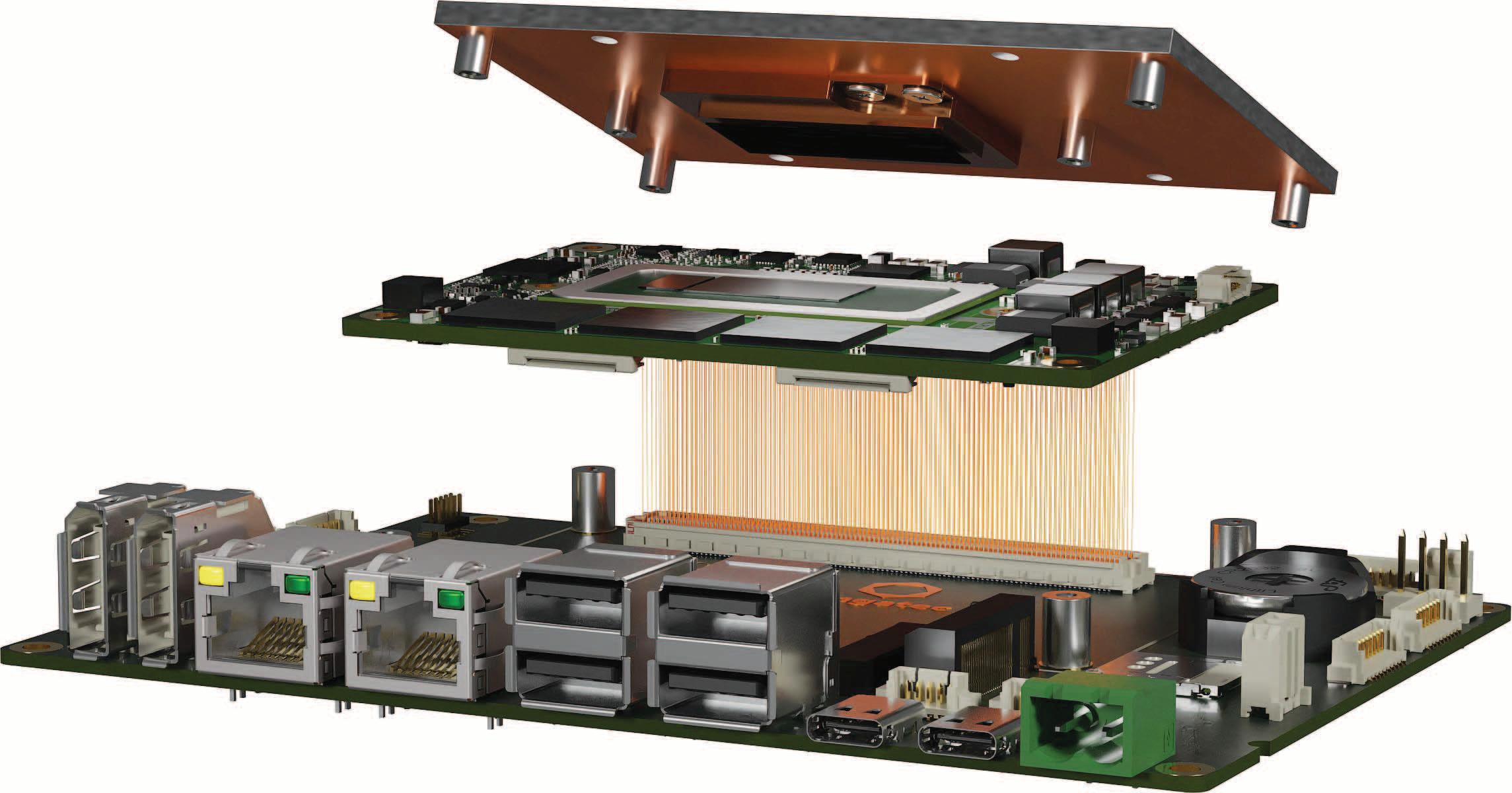
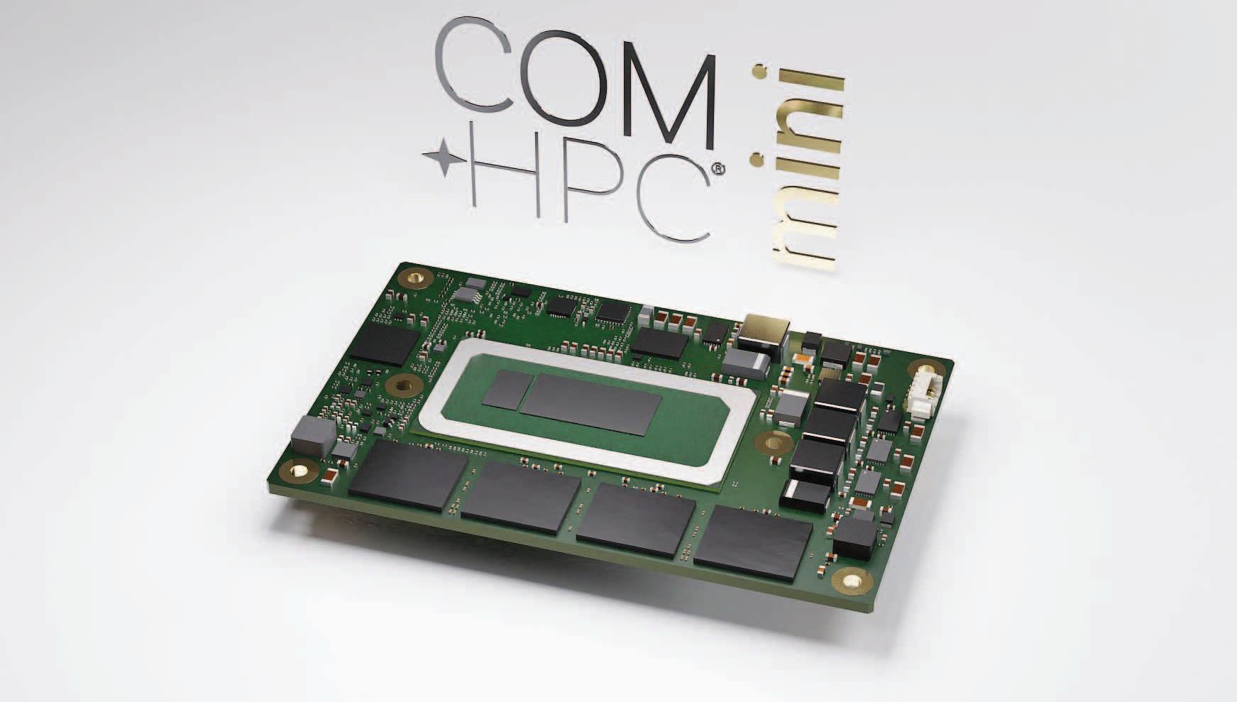
congatec is pleased to announce that the PICMG COM-HPC technical subcommittee has approved the pinout and footprint of the new credit-card-sized (95×60mm) high-performance
Computer-on-Module specification COMHPC Mini. The new COM-HPC Mini standard is now entering the home stretch towards final ratification, which is scheduled for the first half of 2023. Designed for small yet extremely performance-hungry applications the new COM-HPC Mini specification will open up the prospect of developing ultra-powerful microcomputers the size of a 4- or 8-port Ethernet switch, for example. Such small system sizes are needed in many segments of embedded and edge computing. Target markets include box PCs and control cabinet / DINrail PCs, adaptive IoT gateways for the brownfield, cyber-secure edge computers for critical IT/OT infrastructures, rugged tablets, and even ultra-rugged robots and in-vehicle computers wanting to take advantage of the soldered RAM which is a standard feature of these modules.
Processors predestined for this new form factor are the 12th Gen Intel Core processor series – for which congatec already offers a ready-to-deploy design study for initial lab tests and customer feedback loops – and its future successors.
“The pinout approval is an essential milestone as carrier board designers and Computer-on-Module manufacturers such as congatec who are active in the COMHPC working group can now embark on first compliant small form factor sized embedded and edge computer solutions based on this pre-approved data. The goal is to bring modules to market at the same time as Intel and other application processor vendors launch their new high-end processor generations, which is expected to happen next year,” explains Christian Eder, director product marketing congatec, and chairman of the COM-HPC working group
Providing 400 pins, as compared to COM Express Mini’s 220 pins, the new COM-HPC Mini standard is designed to satisfy the rising
interface needs of heterogeneous and multifunctional edge computers. Extensions include up to 4x USB 4.0 with full functionality including Thunderbolt and Display Port alternate mode, PCIe Gen 4/5 with up to 16 lanes, 2x 10 Gbit/s Ethernet port and much more.
Add to that the fact that the COM-HPC Mini connector is qualified for bandwidths of more than 32 Gbit/s – enough to support PCIe Gen 5 or even Gen 6 – it is clear that its capabilities go well beyond those of all other credit-cardsized module standards.
For more information on the new COMHPC Mini Computer-on-Module standard and the congatec COM-HPC Mini design study based on the 12th Gen Intel® Core™ processor series that is pin-compatible to upcoming successors, please visit https://www.congatec.com/en/technologies/com-hpc-mini/. congatec https://www.congatec.com
PICMG, a leading consortium for the development of open embedded computing specifications, announces that the COM-HPC committee has finalized the pinout and dimension definitions for the COM-HPC Mini form factor in record time. This means that the vast majority of the details of the COM-HPC Mini standard have been defined and documentation has already begun. Reaching this critical milestone enables PICMG members to start design work on compliant modules so that embedded OEMs and developers will have access to an elaborated ecosystem shortly after specification launch. The outstanding performance of the 15 member companies in the COM-HPC Mini working group reflects the high market relevance and demand for a high-performance credit-card-sized Computer-onModules standard. Only 12 weeks passed between the approved Statement of Work and the final definition of the mechanics and pinout by the working group.
“The definition of COM-HPC Mini is happening almost at the speed of light. If the working group maintains this performance, and I see no reason to slow it down as there are no
significant technical challenges left to address, I am confident to have a release candidate available for the PICMG release process in Q1 2023, and a published specification by Q2 2023. I anticipate first product announcements will be closely tied to the publication date,” explains Christian Eder, Chairman of the COM-HPC technical committee and Director Product Marketing at congatec.
“The ‘HPC’ in COM-HPC stands for ‘HighPerformance Computing’ but we now use it to refer to the ‘High-Performance Crew’ developing the COM-HPC family of specifications. The team’s performance is keeping pace with the rapidly changing embedded applications and technologies,” adds Jessica Isquith, PICMG President
The COM-HPC Mini pinout specification defines the use of one connector instead of the two implemented for the larger COM-HPC Client and Server modules (Sizes A -E), just like COM Express Mini compared to COM Express Type 6. But with COMHPC, half the number of signal pins still means 400 signal lanes, which equals 90% of the capacity that COM Express Type 6
modules provide. COM-HPC Mini offers a 50% smaller footprint compared to COMHPC Client Size A modules, the currently smallest available COM-HPC form factor. Such extremely small modules measuring only 60 x 95 mm are required for high-end embedded computer logic in devices such as top-hat rail PCs for control cabinets in building and industrial automation, or portable test and measurement devices. In addition, the new specification will enable engineers to integrate state-of-the-art computer interface technologies such as PCIe Gen4 and Gen5 into ultra-small processing units that provide highest performance. As the new specification will come with a focused high-performance pinout and will comply with the entire COM-HPC ecosystem, it is expected to become the high-end standard on top of the PICMG’s earlier COM Express Mini standard. PICMG expects the COM Express specification to continue leading the COM market for many years as it meets numerous standard application requirements now to be allocated in the mid-range performance sector.
PICMG https://www.picmg.org

A mixed-signal PCB design requires basic understanding of analog and digital circuitry to minimize, if not prevent, signal interference. Modern systems consist of components that are operational with both digital and analog domains, and these must be carefully designed to ensure signal integrity all throughout the system.
PCB layout as an important part of the mixed-signal development process can be intimidating and component placement is just the beginning. There are also other factors that must be considered including board layers and how to properly manage these to minimize interferences caused by parasitic capacitors that can be unintentionally created between the interplane layers of the PCB.
Grounding is also an integral process in the PCB layout design of a mixed-signal
This article will detail what to consider when designing the layout of mixed-signal PCBs. It will cover component placement, board layering, and ground plane considerations. The guidelines discussed in this article provide a practical approach to the layout design of mixed-signal boards and should assist engineers of all backgrounds.
system. While grounding is a frequently debated topic in the industry, constructing a standardized approach may not always be the simplest task for any engineer. For instance, a single issue of quality grounding can affect the entire layout of a high performance mixed-signal PCB design. And for this reason, this area should not be overlooked.
Similar to building a house, it is essential to create a floor plan of the system before placing the circuit components.
This step will set the overall integrity of the system design and should help avoid noisy signal interference. In developing a floor plan, it is advisable to follow the signal path of the schematic, especially for high speed circuits.
The location of a component is also a critical aspect of the design. The designer should be able to identify the important functional block, signals, and the connection between the blocks in order to identify the best fit location of each component in the system. Connectors, for instance, are better placed on the edges of the board, while auxiliary components such as decoupling capacitors and crystals must be placed as close as possible to the mixed-signal device.
To help minimize the common return path for analog and digital signals, analog and digital block separation may be considered such that analog signals will not mix with digital signals.
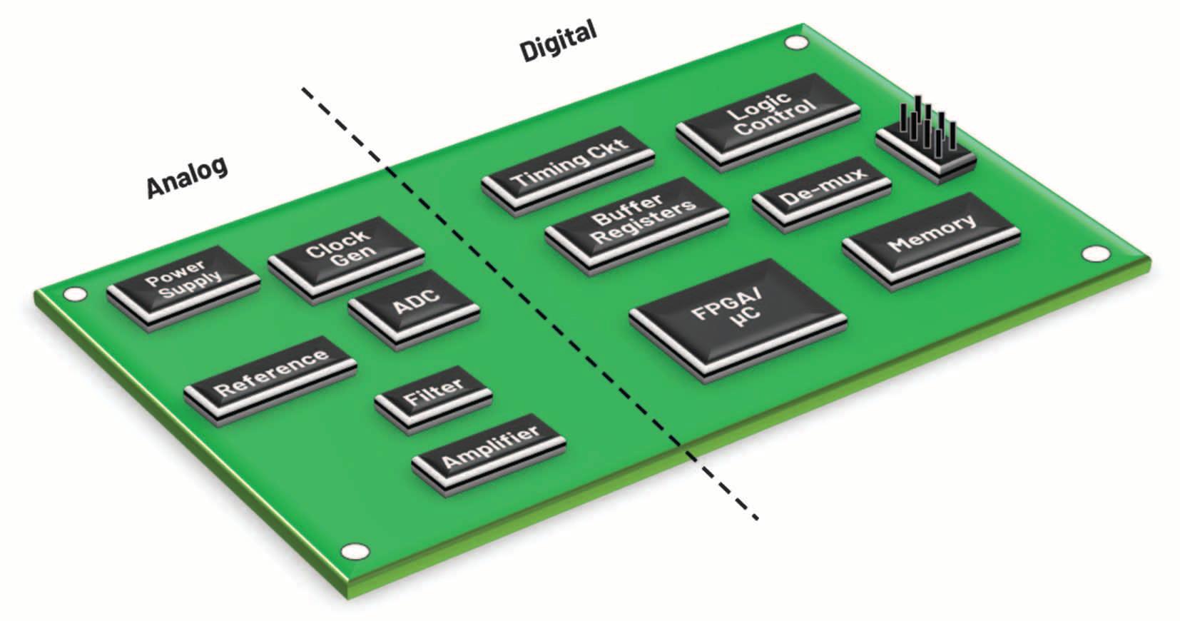
Figure 1 shows a good example of analog and digital circuit separation. Some considerations when separating analog and digital sections are:
• Sensitive analog components such as amplifiers and voltage references are recommended to be placed within the analog plane. Similarly, the noisy digital components such as logic controls and timing blocks must be placed on the other side/digital plane.
• If a system contains one mixed-signal analog-to-digital converter (ADC) or a digital -to-analog converter (DAC) with low digital currents, this can be treated similar to analog components that are included in the analog plane.
• For designs with more than one ADC and DAC with high current, it is recommended to split the analog and digital supplies. That is, AVCC must be tied to the analog section while DVDD should be connected to the digital section.
• Microprocessors and microcontrollers may take up space and will generate heat. These components must be placed in the center of the board for better thermal dissipation, and, at the same time, close to their related circuit blocks.
The power supply is an important part of the circuit and should be handled accordingly. As a rule of thumb, the power supply block must be isolated from the rest of the circuitry and at the same time remain close to the components being powered.
Complex systems with devices that have multiple supply pins can use separate power supply blocks dedicated for the analog and digital sections to avoid noisy digital interference.
On the other hand, power supply routing should be short, direct, and use wide traces to reduce inductance and avoid current limitation.
Power supply rejection ratio (PSRR) is one of the important parameters a designer must consider in achieving target system performance. PSRR is the measure of the sensitivity of a device with respect to power supply variations, which will eventually dictate the performance of a given device.
To maintain an optimum PSRR, it is necessary to keep the high frequency energy from entering the device. This can be done by properly decoupling the power supply of the device to the low impedance ground plane with a combination of electrolytic and ceramic capacitors.
The whole concept of correct decoupling is to develop a low noise environment in which the circuit can operate. The basic rule is to make it easy for the current to return by providing the shortest path.
Designers must always check the high frequency filtering recommendation of each device. More so, this checklist will serve as a guide by providing general decoupling techniques and their correct implementation:
• While electrolytic capacitors act as charge reservoirs to transient currents to minimize low frequency noise on power
supplies, low inductance ceramic capacitors on the other hand reduce high frequency noise. Also, ferrite beads are optional but will add extra high frequency noise isolation and decoupling.
• Decoupling capacitors must be placed as close as possible to the power supply pins of the device. These capacitors should connect to a large area of low impedance ground plane through a via or short trace to minimize additional series inductance.
• The smaller capacitor, typically 0.01 μF to 0.1 μF, should be placed as close as physically possible to the power pins of the device. When the device has several outputs switching at the same time, this placement prevents instabilities. The electrolytic capacitor, typically 10 μF to 100 μF, should be placed no more than one inch away from the power pin of the device.
• For easier implementation, decoupling capacitors can be linked through a T-type connection to the ground plane using vias near the GND pin of the component rather than creating a trace. See the sample in Figure 2.
Once component placement and the floor plan have been set, we can go through the other dimension of the board design, which is commonly referred to as board layers. It is highly recommended that board layers should be considered first before doing the PCB routing as this will determine the allowable return current paths of the system design. A board layer is the vertical arrangement of the copper layers in the board. These layers should manage the currents and signal throughout the board.
Figure 3: A sample 4-layer PCB.
PCBs
A visual representation of the board layers is shown in Figure 3. Table 1 details a typical 4-layer PCB setup:
1 Digital/analog signal (top layer)
2 Ground 3 Power plane
4 Aux signal (bottom layer)
Table 1: Typical 4-Layer PCB.
In general, high performance data collecting systems should have four or more layers. The top layer is often used for digital/analog signals, while the bottom layer is used for auxiliary signals. The second layer (ground layer) serves as a reference plane for impedance-controlled signals and used for reducing IR drops and shielding the digital signals in the top layer. Finally, the power plane is on the third layer.
Power and ground planes must be adjacent to each other as they provide additional interplane capacitance, which helps with the high frequency decoupling of the power supply.
For the ground layer, advice has changed over the years for the mixed-signal design. Over the years, splitting the ground plane between analog and digital has made sense but for modern mixed-signal devices, a new approach is recommended. Proper floor planning and separating signals should prevent any issues with noisy signals.
Grounding is an essential process in the layout design of a mixed-signal PCB. A typical 4-layer PCB must have at least one layer dedicated to the ground plane to ensure a low impedance path for return signals. All integrated circuit ground pins should be routed and connected correctly to the low impedance ground plane to minimize the series inductance and resistance.
It has become a standard grounding approach for mixed-signal systems to separate analog and digital ground. However, mixed-signal devices with low digital current can be best managed with a single ground. Moving forward, a designer must consider which grounding practice suits best depending on the mixed-signal current requirement. There are two grounding practices a designer must consider.
For mixed-signal systems with a single ADC or DAC with low digital current, a solid single ground plane would be the best approach. To understand the importance of a single ground layer, we need to recall return current. Return current is the current that flows while returning to ground and traces between devices to complete a loop. To prevent mixed-signal interference, each return path must be tracked throughout the PCB layout.
For low frequency signals, the return current will take the path of least resistance, usually a straight line between the ground reference points of the devices.
However, for higher frequency signals, a certain portion of the return current will try to follow the signal path back. This is because the impedance is lower following this path since it minimizes the size of the loop formed between the outgoing and returning current.
Figure 4: Return current for system with a solid ground plane. © ADI
Figure 5: Return current for systems with a split ground plane.
The simple circuit in Figure 4 shows the advantage of a single solid ground plane over a split ground plane. The signal current has an equal but opposite flow of return current. This return current flows in the ground plane back to the source and it will follow the path of least impedance.
For complex systems where a solid ground scheme can be challenging to achieve, a split ground may be more appropriate. A split ground plane is another popular approach where the ground plane is split in two: analog and digital ground planes.
This is applicable for more complex systems with multiple mixed-signal devices consuming high digital current. Figure 5 shows an example of a system with a split ground plane.
For systems with a split ground plane, the simplest solution to achieve a cohesive ground is to remove the break in the ground planes and allow the return current to take a more direct route through a star ground junction. The star ground is the junction where the analog and digital ground planes are joined together on a mixed-signal layout design.
In common systems, the star ground can be associated with a simple narrow continued junction in between analog and digital ground planes. For more complex designs, the star ground is commonly implemented with a jumper shunt to a ground header. No high current carrying a header and jumper shunt is required as there will be no flow of current in the star ground, but rather its main purpose is to make sure that both grounds have the same reference levels.
Designers must always check grounding recommendations found in each device’s data sheet to ensure grounding specifications will be met and avoid ground related issues. On another note, for mixed-signal devices that have AGND and DGND pins, these can be tied to their respective ground planes since the star ground will also connect both grounds at one point.
In this way, all noisy digital currents will flow through the digital power supply down to the digital ground plane and back to the digital supply all the while being isolated from the sensitive analog circuitry. Isolation of the AGND and DGND planes must be implemented on all layers of a multilayer PCB.
Here is a procedure/checklist that one can follow to ensure an appropriate grounding scheme has been implemented in a mixed-signal analog/digital system:
• Wide copper traces should make up the connections at the star point.
• Check the ground plane for narrow traces, as these connections are undesired.
• It is useful to provide pads and vias so that the analog and digital ground planes can be connected, if necessary.
The PCB layout for mixed-signal applications can be challenging. Creating a component floor plan is just the starting point. Properly managing board layers and preparing an adequate grounding scheme are also part of the key points a system designer must consider when trying to achieve optimum performance in a mixed-signal system layout.
Preparing a component floor plan will help set the overall integrity of the system design.
Proper board layer organization will help manage the currents and signal throughout the board. Finally, choosing the most beneficial grounding scheme will improve the system’s performance and prevent any issues with noisy signals and return current.
The material presented in this article was compiled from many contributors, including Eric Carty, Genesis Garcia, Giovanni Aguirri, Brendan Somers, Stuart Servis, Leandro Peje, Mar Christian Lacida, and Yoworex Tiu.
■ Analog Devices www.analog.com

May Anne Porley is an applications engineer at Analog Devices, Philippines, within the Automated Test Equipment (ATE) Group. She joined ADI in 2012 and provides applications support for switches, multiplexers, level translators, and unbuffered crosspoint switches portfolios.

May Anne graduated from De La Salle University - Dasmariñas, Philippines, with a bachelor’s degree in electronics engineering.
Kevin Chesser was a product application engineer with the SMX Group at ADI, Limerick. He is very passionate about electronics and the real-world problems that can be solved using technology.

Kevin provided customer support focusing on the ADG7xx family of switches and multiplexers.
Walt Kester. The Data Conversion Handbook. Analog Devices, Inc., 2005.
John Ardizzoni. “A Practical Guide to HighSpeed Printed-Circuit-Board Layout.” Analog Dialogue, Vol. 39, No. 9, Sept. 2005.
Ralph Morrison. Grounding and Shielding Techniques. John Wiley & Sons, Inc., 1998.
Thomas O’Shea. “AN-1349 Application Note: PCB Implementation Guidelines to Minimize Radiated Emissions on the ADM2582E/ADM2587E RS-485/RS-422 Transceivers.”
Analog Devices, Inc., August 2018.
“MT-101 Tutorial Decoupling Techniques.” Analog Devices, Inc., 2009.
Linear Circuit Design Handbook. Analog Devices, Inc., 2008.
Paul Brokaw. “AN-342 Application Note, Analog Signal-Handling for High Speed and Accuracy.” Analog Devices, Inc.
Walt Kester, James Bryant, and Mike Byrne. “MT-031 Tutorial Grounding Data Converters and Solving the Mystery of ‘AGND’ and ‘DGND’.” Analog Devices, Inc., 2009.
Paul Brokaw and Jeff Barrow. “AN-345 Application Note: Grounding for Low- and High-Frequency Circuits, Know Your Ground and Signal Paths for Effective Designs, Current Flow Seeks Path of Least Impedance–Not Just Resistance.” Analog Devices, Inc.
Doug Grant and Scott Wurce. “AN-348 Application Note: Avoiding Passive Component Pitfalls, The Wrong Passive Component Can Derail Even the Best Op Amp or Data Converter Here Are Some Basic Traps to Watch For.” Analog Devices, Inc.
Engage with like-minded members and ADI technology experts in our online community, EngineerZone®. Expand your network, ask your tough design questions, share your expertise, browse our rich knowledge base, or read about new technologies and the engineers behind them in one of our blogs.

Visit https://ez.analog.com
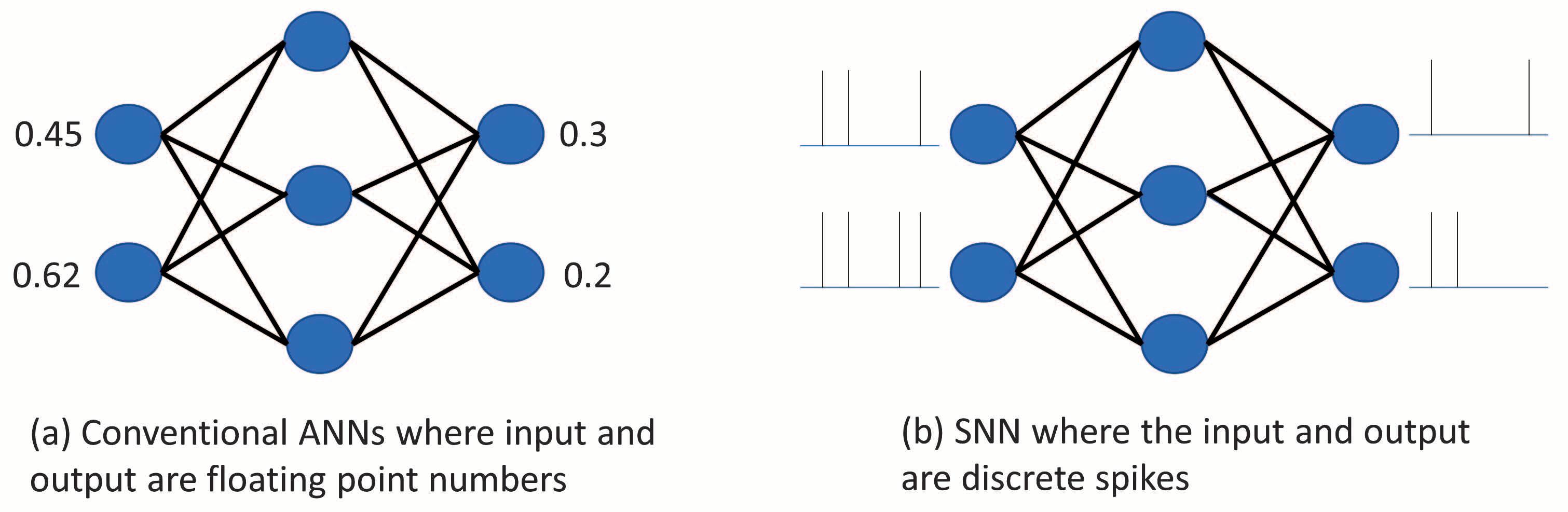
Neural networks (NN) have been inspired by the brain and using neuroscience terminologies (neurons and synapses) to explain neural networks has always given grievance to neuroscientists as the current generation of neural networks are poles apart from how the brain operates. Despite the inspiration, the general structure, neural computations, and learning techniques between the current second generation of neural networks and the brain vastly differed. This comparison annoyed neuroscientists so much that they started working on the third generation of networks that more closely resembled the brain, called spiking neural networks (SNN) with hardware capable of executing them, that is neuromorphic architecture.
Author: Eldar Sido Product Marketing Specialist Renesas Electronics

Spiking neural networks
SNNs are a type of artificial neural network (ANNs) that are more closely inspired by the brain than their second-generation counterpart with a key difference in that SNNs are spatiotemporal NNs i.e., they consider timing in their operation. SNNs operate on discreet spikes determined by a differential equation representing various biological processes. The critical one is firing after the neuron's membrane potential (“firing” threshold) is reached, which occurs by spikes being fired at that neuron at specific time sequences. Analogously, the brain consists of 86 billion computa-
tional units called neurons, receiving input from other neurons via dendrites, once the inputs exceed a certain threshold, the neuron fires and send an electric pulse via a synapse, and synaptic weight control the extent of the pulse sent to the next neuron. Unlike other artificial neural networks, SNN neurons fire asynchronously at different layers throughout the network arriving at different times where traditionally, the information propagates throughout the layers dictated by the systems clock. The spatiotemporal property of SNNs along with the discontinuous nature of spikes means that the models can be more
sparsely distributed with neurons only connecting to relevant neurons and using time as a variable, allowing for information to be encoded more densely versus traditional binary encoding of ANNs. Leading to SNNs being more powerful computationally and more efficient.
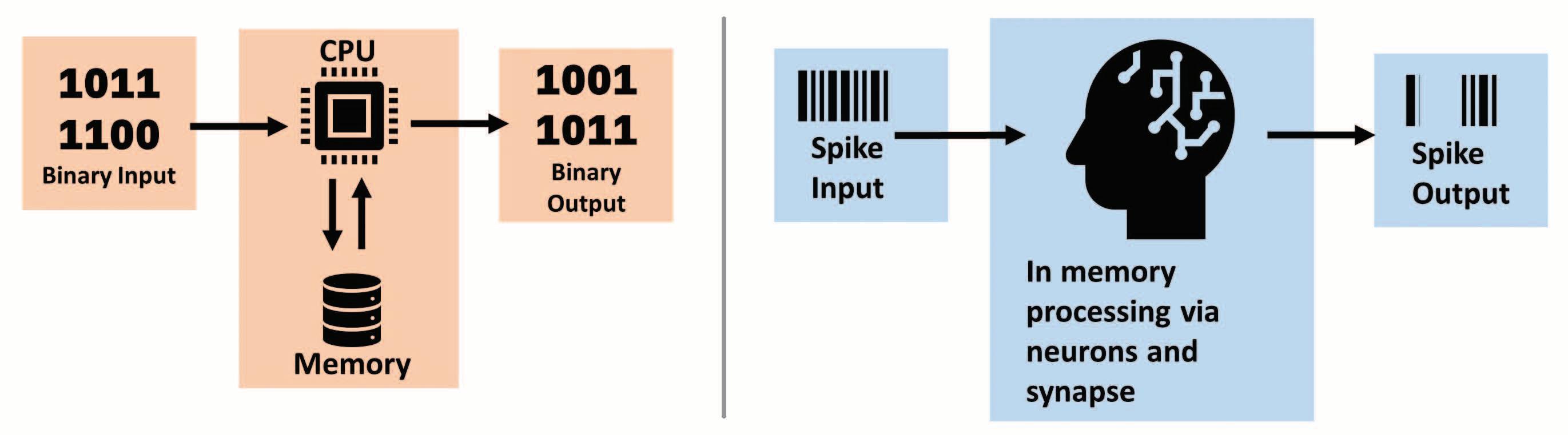
The asynchronistic behavior of SNNs along with the need of executing differential equations is computationally demanding on traditional hardware and new architecture had to be developed. This is where neuromorphic architecture comes in.

Neuromorphic architecture is a non-von Neuman architecture inspired by the brain, composed of neurons and synapses. In neuromorphic computers, the processing and storing of the data occurs in the same region, alleviating the Von Neuman bottleneck that slows down the maximum throughput traditional architectures can achieve due to the need of moving data from memory to processing units at relatively slow rates. In addition, neuromorphic architecture natively supports SNNs and
coming age of edge and endpoint AI.
To understand the expected demand from the industry, a look at research forecasts is necessary. According to a report by Sheer Analytics & Insights, an expectation that the worldwide market for neuromorphic computing to reach $780 million with a CAGR of 50.3 percent by 2028[1]. Mordor Intelligence, on the other hand, expects the market to reach $366 million by 2026 with a CAGR of 47.4 percent[2] and much more market research can be found online indicating a similar increase.
natural step to incorporate a neuromorphic core for TinyML use cases as there are several distinct advantages.
Neuromorphic devices are event-based processors operating on non-zero events. Event-based convolution and dot products are significantly less computationally expensive as zeroes are not processed.
Event-based convolution performance improves further with the larger number of zeroes in the filter channels or kernels.
accepts spikes as inputs, allowing information to be encoded in the spikes’ time of arrival, magnitude, and shape. Thus, the key features of neuromorphic devices include their inherent scalability, event-driven computation, and stochasticity as neurons firing can have a sense of randomness making neuromorphic architecture attractive due to their ultra-low power operation, usually operating magnitudes less than traditional computing systems.
Neuromorphic market forecast
Technologically, neuromorphic devices have the potential to play a big role in the
While the forecast numbers are not consistent with each other, one thing is consistent, the demand for neuromorphic devices is expected to drastically increase in the coming few years and market research companies expect various industries such as industrial, automotive, mobile, and medical to adopt neuromorphic devices for a variety of applications.
As TinyML (tiny machine learning) is all about executing ML and NNs on tightly memory/ processor constrained devices such as microcontrollers (MCU), it is a
This along with activation functions such as Relu being centered around zero provides the property of event-based processors’ inherent activation sparsity, thus reducing effective MAC requirements.
Furthermore, as neuromorphic devices’ process spikes, more constrained quantization can be used such as 1-,2- and 4-bit quantization, as compared to the conventional 8-bit quantization on ANNs. Moreover, since SNNs are incorporated into hardware, neuromorphic devices (such as Akida from Brainchip) have the unique capability of on-edge learning.
This is not possible with conventional devices as they only simulate a neural network with Von Neumann architecture leading to on-edge learning being computationally expensive with large memory overheads, out of a TinyML systems budget.
In addition, for training a NN model, integers would not provide enough range to train a model accurately so training with 8bits is not currently feasible on traditional architectures. For traditional architectures, currently, a few on-edge learning implementations with machine learning algorithms (autoencoders, decision trees) have reached a production stage for simple realtime analytics use cases, whereas NNs are still under research.
To summarize, the advantages of using neuromorphic devices and SNNs at the endpoint:
• Ultra-low power consumption (milli to microjoule per inference)
• Lower MACs requirements as compared to conventional NNs
• Lower parameter memory usage as compared to conventional NNs
• On-edge learning capabilities
With all said and done, microcontrollers with neuromorphic cores can excel in use cases throughout the industry with their distinct characteristics of on-edge learning such as:
• In anomaly detection applications for existing industrial equipment, where using the cloud to train a model is inefficient, so adding an endpoint AI device on the motor and training on the edge would allow ease of scalability as equipment aging tends to differ from machine to machine even if they are the same model.
• In robotics, as time passes, the joints of robotic arms tend to wear down, becoming untuned and stop operating as needed. Re-tuning the controller on the edge without human intervention mitigates the need to call a professional, reducing downtime, and saving time and money.
• In face recognition applications, a user would have to add their face to the dataset and retrain the model on the cloud. With a few snaps of a person’s face, the neuromorphic device can

identify the end-user via on-edge learning. Allowing users’ data to be secured on the device along with a more seamless experience. This can be used in cars, where different users have different preferences on seat position, climate control, etc.
• In keyword spotting applications, the addition of extra words for your device to recognize on the edge. Can be used in biometric applications, where a person would add a “secret word” that they would want to keep secure on the device.
The balance of ultra-lower power of neuromorphic endpoint devices and enhanced performance makes it suitable for prolonged battery-powered applications, executing algorithms not possible on other low-power devices due to them being computationally constrained. Or vice versa with higher-end devices capable of similar processing power being too power-hungry. Use cases include:
• Smartwatches that monitor and process the data at the endpoint, sending only relevant information to the cloud.
• Smart camera sensors for people detection to execute a logical command. For instance, automated door opening when a person is approaching as current technology is based on proximity sensors.

• Area with no connectivity or charging capabilities such as in forests for smart animal tracking or monitoring under ocean pipes for any potential cracks using real-time vibration, vision, and sound data.
• For infrastructure monitoring use cases, where a neuromorphic MCU can be used to continuously monitor movements, vibrations, and structural changes in bridges (via images) to identify potential failures.
[1]
“Renesas as a leader in semiconductors has acknowledged the vast potential of neuromorphic devices and SNNs that we have licensed a neuromorphic core from Brainchip[3], the world’s first commercial producer of neuromorphic IP”, as noted by Sailesh Chittipeddi, Executive Vice President and General Manager of the IoT and Infrastructure Business Unit of Renesas. “At the very low end, we have added an ARM M33 MCU and spiking neural network with BrainChip core licensed for selected applications – we have licensed what we need to license from BrainChip including the software to get the ball rolling.” 4]
Thus, as Renesas tries to innovate and develop the best possible devices into the market, the company is excited to see how this innovation will contribute to making lives easier.
About the author: Eldar Sido works in the product marketing management team for the ARM based MCU family at Renesas Electronics. Specializing in technical aspect of endpoint AI implementation on microcontrollers. He received his master's degree from The University of Tokyo in nanotechnology.

■ Renesas www.renesas.com

“Neuromorphic computing market – industry analysis, size, share, growth, trends, and forecast, 2020-2028.,” sheeranalyticsandinsights.com. [Online].
Available: https://www.sheeranalyticsandinsights.com/market-report-research/neuromorphic-computing-market-21/ [Accessed: 23-Aug-2022].
[2]
“Neuromorphic chip market growth, forecast (2022-27): Industry trends,” Neuromorphic Chip Market Growth, Forecast (2022-27) | Industry Trends. [Online].
Available: Neuromorphic Chip Market Growth, Forecast (2022-27) | Industry Trends (mordorintelligence.com). [Accessed: 23-Aug-2022].
[3]
“BrainChip's Akida set for spaceflight via NASA as Renesas Electronics America signs First IP agreement,” Small Caps, 23-Dec-2020. [Online].
Available: BrainChip’s Akida set for spaceflight via NASA as Renesas Electronics America signs first IP agreement (smallcaps.com.au). [Accessed: 23-Aug-2022].
[4] Arm battles RISC-V at Renesas. [Online]. Available: ARM battles RISC-V at Renesas - eeNews Europe. [Accessed: 23-Aug-2022].


This article briefly describes the requirements for high-accuracy temperature measurements in mobile and battery-powered health monitoring applications. It then introduces a low-power, high-accuracy digital temperature sensor IC from ams OSRAM that doesn’t require calibration or linearization. It finishes with integration recommendations, an evaluation board, and a Bluetooth-enabled demo kit with a companion app that makes it possible to modify sensor settings and observe the impact on power consumption.
Author: Rolf Horn | Applications Engineer Digi-Key Electronics
Accurate digital temperature measurements are important in a range of applications including wearables, medical monitoring devices, health and fitness trackers, cold chain and environmental monitoring, and industrial computing systems. While widely applied, the implementation of highly accurate digital temperature measurements frequently involves temperature sensor calibration
or linearization, as well as higher power consumption which can be an issue for compact, ultra-low power applications with multiple acquisition modes.
The design challenges can quickly mount, causing cost overruns and delayed schedules.
Complicating the matter, some applications involve multiple temperature sensors sharing a single communication bus.
In addition, some production test setups need to be calibrated according to the U.S. National Institute of Standards and Technology (NIST), while verification equipment needs to be calibrated by an ISO/IEC-17025 accredited laboratory.
Suddenly, what seemed a straightforward function becomes both intimidating and costly.
Requirements for high-accuracy temperature monitoring
Accuracy is mandatory in health monitoring applications. As manufactured, digital temperature sensors exhibit part-to-part variations in performance that need to be addressed.
As in-house calibration is expensive and using uncalibrated sensors increases the cost of achieving the desired accuracy, designers should consider sensors that are fully calibrated and linearized. It is, however, important to ensure that the sensor maker uses calibration instruments traceable to NIST standards.
Using instruments with traceable calibration ensures an unbroken chain back to the basic NIST standards, with the uncertainties at each link in the chain identified and documented so they can be addressed in the device maker’s quality assurance system.
The primary standard for testing and calibration laboratories is ISO / IEC 17025
“General requirements for the competence of testing and calibration laboratories.” ISO / IEC 17025 is based on technical principles focused specifically on cali bration and testing laboratories, is used for their accreditation, and provides the basis for developing continuous improvement plans.
Digital temperature sensor with NISTtraceable production testing
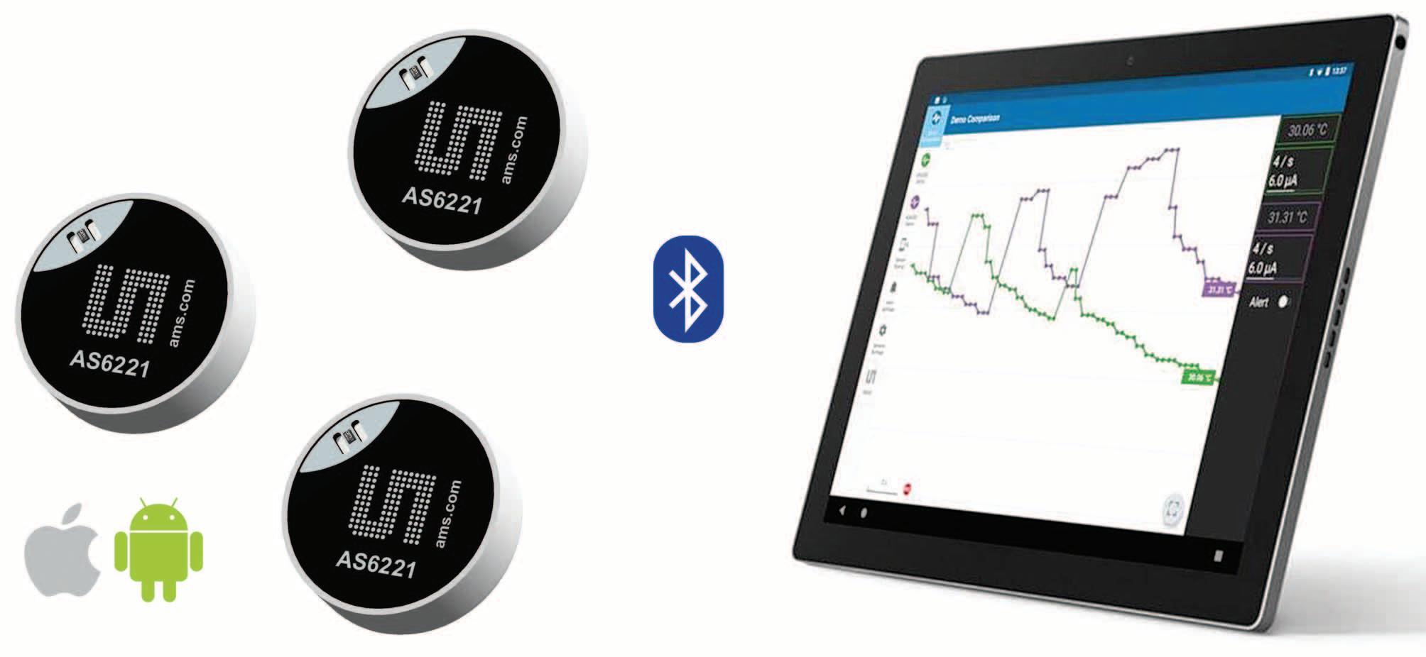
To meet the many design and certification requirements, designers can turn to the AS6211 digital temperature sensor from ams OSRAM that provides accuracy up to ±0.09°C and requires no calibration or linearization. Designed for use in healthcare devices, wearables and other applications that require high-performance thermal information, the AS6211’s production testing is calibrated by an ISO/IEC-17025 accredited laboratory according to NIST standards.
The calibrated production testing speeds the process of gaining certification to EN 12470-3, which is required for medical thermometers in the European Union. The AS6211 is a complete digital temperature sensor in a six-pin, 1.5 × 1.0-millimeter (mm) wafer level chip scale package (WLCSP), ready for system integration. An orderable part number example, the AS6221-AWLT-S, is delivered in lots of 500 pieces on tape & reel. The AS6211’s measurements are delivered through a standard I²C interface, and it supports eight I²C addresses, thereby eliminating concerns about bus conflicts in multi-sensor designs.
It includes a sensitive and accurate silicon (Si) bandgap temperature sensor, an analog-to-digital converter, and a digital signal processor with associated registers and control logic. The integrated alert function can trigger an interrupt at a specific temperature threshold, which is programmed by setting a register value.
The AS6221 consumes 6 microamperes (μA) when making four measurements per second, and in standby mode, power consumption is only 0.1 μA. The use of the integrated alarm function to wake up the application processor only when a temperature threshold has been reached can reduce system power consumption even more.

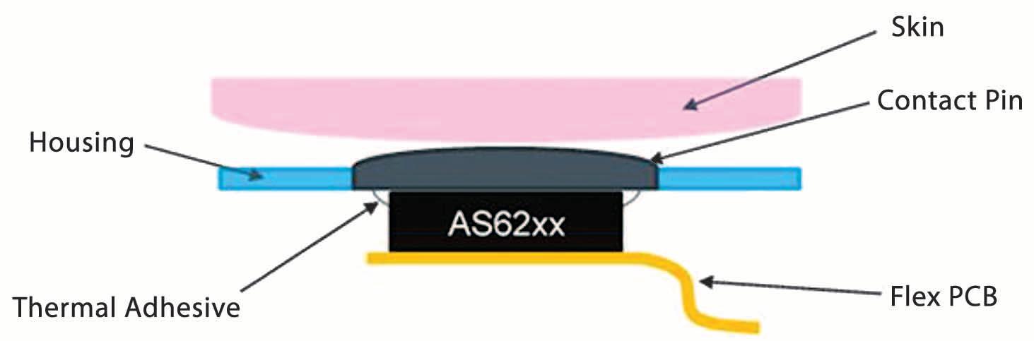
In wearable applications, the better the thermal connection between the sensor and the skin, the more accurate the temperature measurement. Designers have several options for optimizing the thermal connection. One way is to put a thermally conductive pin between the skin and the sensor (Figure 1).
To achieve reliable results, the pin needs to be isolated from any external sources of thermal energy, such as the device case, and a thermal paste or adhesive should be used between the pin and the AS6211. This approach benefits from using a flexible (flex) printed circuit board (PCB) to carry the AS6221, enabling more freedom in locating the sensor.
In designs that benefit from having the sensor on the main PCB, the thermal connection can be made using a contact spring or a thermal pad.
The AS6221 delivers high accuracy with low power consumption over its full supply range from 1.71 to 3.6 volts DC, which is especially important in applications powered by a single battery cell.
If the sensor is mounted on the bottom of the PCB, a contact spring can be used to make a thermal connection between the contact pin and thermal vias on the PCB that are connected to the sensor (Figure 2).
This approach can result in a cost-effective device that supports longer distances between the sensor and the skin, but it requires careful consideration of the several thermal interfaces to achieve high levels of sensitivity.
mechanical design to ensure minimum thermal impedance between the contact pin and the sensor.
This can result in a simpler assembly while still delivering high levels of performance.
Two viable design suggestions are to use cutouts to minimize any copper planes in the vicinity of the sensor on the top of the PCB (Figure 4, top), and to reduce thermal loading from the bottom of the PCB by using a cutout area below the sensor to reduce overall PCB mass (Figure 4, bottom).
In addition to minimizing PCB effects, other techniques that can help improve measurement speed and performance include:
• Maximizing the contact area with the skin to increase the heat available to the sensor.
Figure 2
When the sensor is mounted on the bottom of a PCB, thermal vias and a contact spring can be used to connect to the contact pin.
• Using thin copper traces and minimizing the size of power and ground planes.
• Using batteries and other components such as displays that are as small as possible to achieve the device performance requirements.
• Designing the package to thermally isolate the sensor on the PCB from the surrounding components and the outside environment.
Sensing environmental temperature
Figure 3
A thermal pad can connect a top-mounted sensor to the contact pin. This provides simpler assembly, while still delivering high performance.
A third option is to use a thermal pad to connect the pin to a sensor mounted on the top of the PCB (Figure 3).
Compared with using a spring contact or flex PCB, this approach requires a pad with high thermal conductivity and careful
In order to obtain fast thermal response times, it’s important to minimize the external influences on the measurement, especially by the portion of PCB directly adjacent to the sensor.
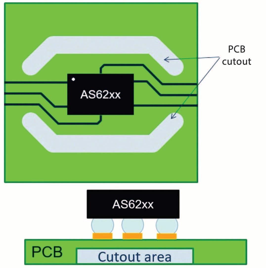
Figure 6
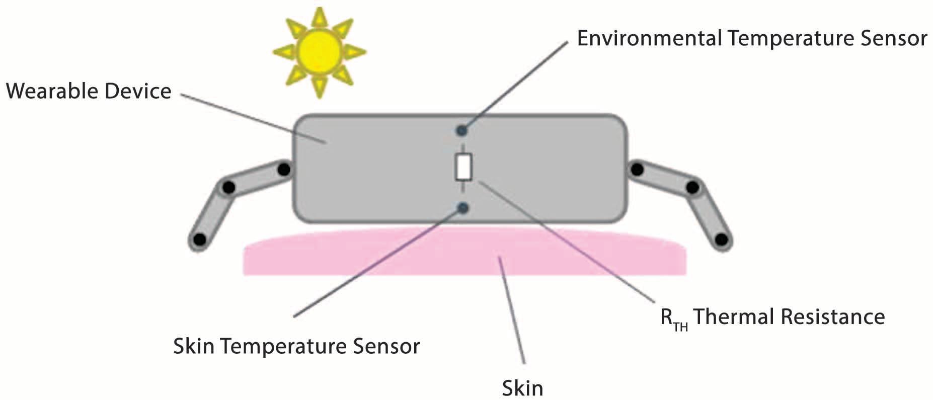
Additional considerations apply when using multiple temperature sensors, such as in designs that use both skin temperature and the temperature of the surrounding environment.
A separate sensor should be used for each measurement. The thermal design of the device should maximize the thermal impedance between the two sensors (Figure 5).
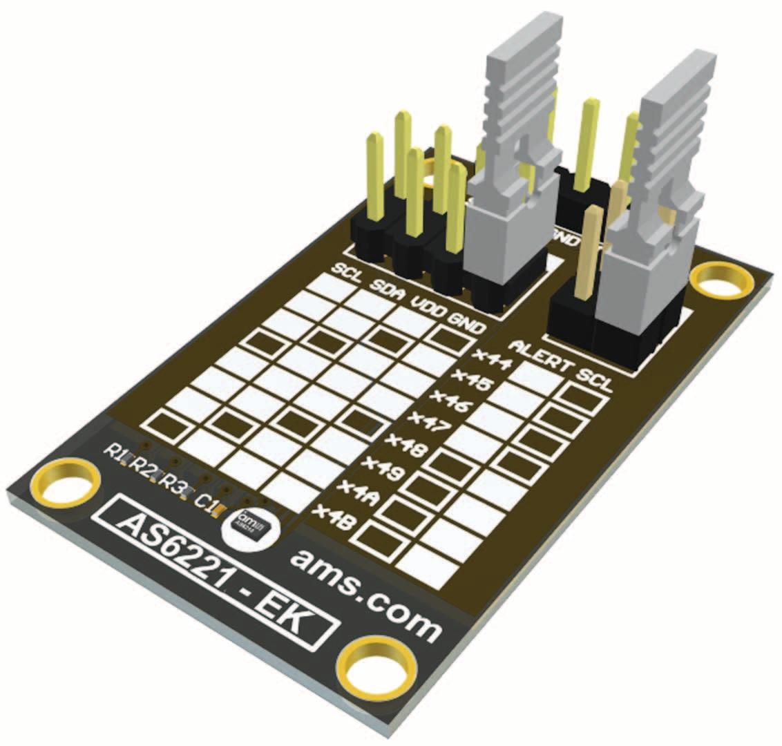
The AS62xx eval kit can be used to set up and evaluate the AS6221.
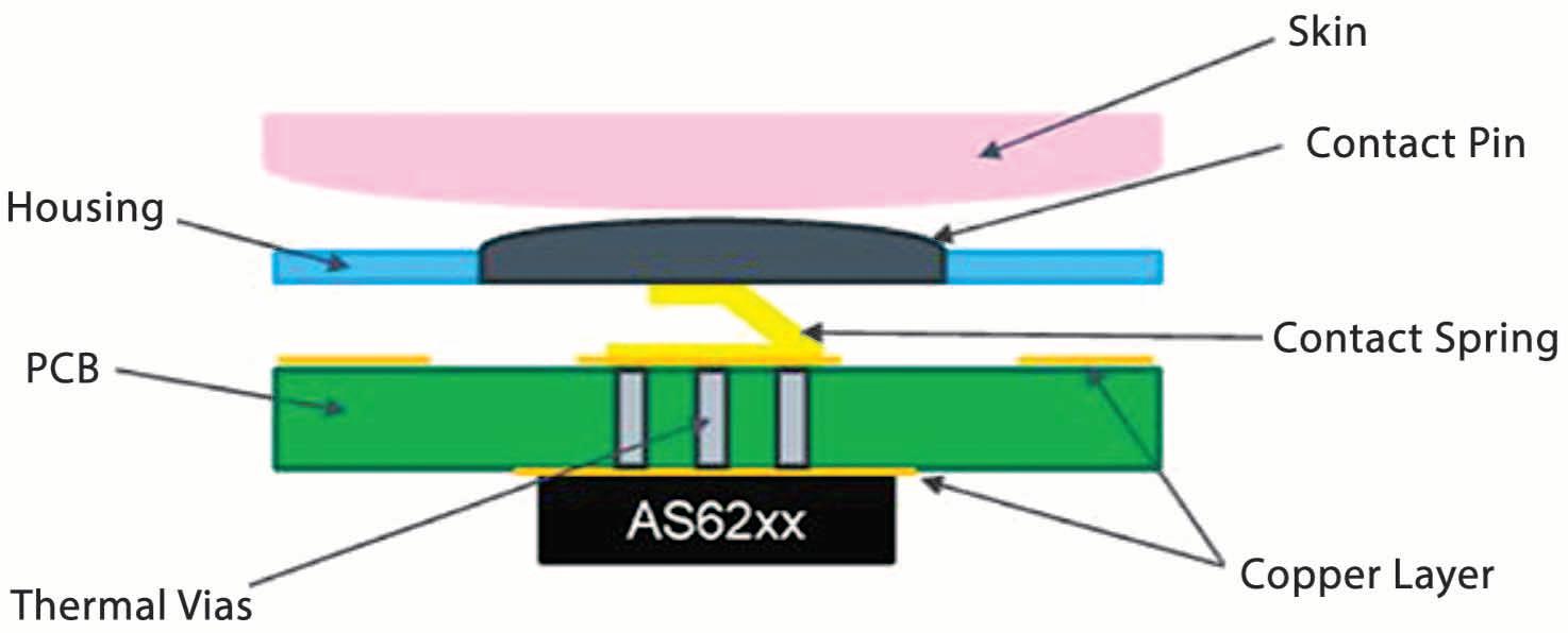
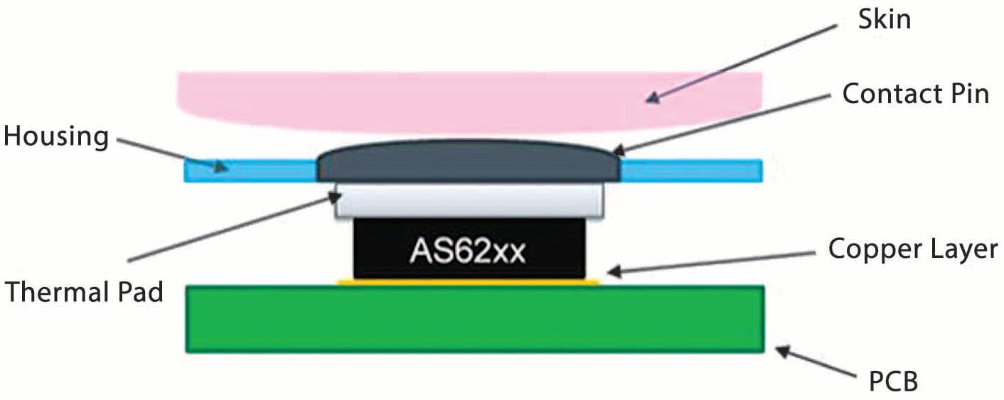
Figure 4
Cutouts on the top and bottom of the PCB can minimize the PCB mass around the sensor and improve its response time.
A higher intervening thermal impedance provides better isolation between the sensors and ensures that the measurements will not interfere with one another. The device package should be fabricated with materials that have low thermal conductivities, and a thermal isolation barrier should be inserted between the two sensor sections.
Demo kit for the AS6221
Once the basic evaluation is completed, designers can turn to the AS6221 demo kit as an application development platform. The demo kit includes an AS6221 temperature button and a CR2023 coin cell battery. Downloading the companion app from the App Store or Google Play Store supports connection to up to three sensor
©
Figure 5
For accurate environmental temperature sensing, there should be a high thermal resistance between the skin and environmental temperature sensors.
Eval kit kickstarts AS6221 development
To speed application development and time to market, ams OSRAM offers designers both an eval kit and a demo kit. The AS62xx Eval Kit can be used to quickly set up the AS6221 digital temperature sensor, enabling a quick evaluation of its capabilities. This eval kit connects directly to an external microcontroller (MCU) that can be used to access temperature measurements.
buttons at one time (Figure 7). The app communicates with the sensor buttons over Bluetooth, making it possible to modify all of the sensor settings, including the measurement frequency, and observe the impact on power consumption.
The app can record measurement sequences, thereby enabling comparisons of the performance of various temperature sensor settings.
Designers can also use the demo kit to experiment with the alert mode and learn how it can be used to improve solution performance.
Designing high-accuracy digital temperature sensing systems for healthcare, fitness, and other wearables is a complex process with respect to design, test, and certification. To simplify the process, lower cost, and get to market more quickly, designers can use highly integrated, lowpower, high-accuracy sensors.
As shown, the AS6221 is one such device. It does not require calibration or linearization, and the production testing equipment is calibrated according to NIST standards by an ISO/IEC-17025 accredited laboratory, speeding the design and approval process for medical devices.
Recommended Reading
• Enhance Battery Life in Wearables Through Efficient Timekeeping During Idle States
• Use Adjustable Low Leakage LDOs to Extend Battery Life in Wearable Designs
• Boost Fitness Tracker Accuracy Using High-Accuracy Pressure Sensors
■ Digi-Key Electronics www.digikey.com


The 4HP PXI nVent carriers with congatec COMs are much flatter than classic 8HP or 12HP assemblies.
Test systems for electronics manufacturing are often modular constructions, plugging together multiple PCI Express-based cards. What technicians assembling such modular systems have been missing so far are ultra-slim CPU boards that would allow them to pack more measurement cards into a system. Thanks to a collaboration between nVent and con gatec, such cards are now available.

PXI users are test and measurement system experts whose primary focus is on the test software and the various I/Os. The central controllers are simply a means to an end for them. Which is why they often use a standard notebook or desktop PC to connect to a PXI measurement system that just offers expansion cards. Alternatively, they may use a PXI controller module. However, as these are commonly designed to meet virtually all needs of all types of applications, they are often overspecified.
So today, the majority of 3U PXI boards are 8HP or 12HP wide even though 4HP would in principle suffice.
CPU boards in widths of 8HP or 12HP can quickly block two or three slots, meaning systems would either need to be wider or not have sufficient free expansion slots to handle all the various test and measurement tasks.
It is therefore often desirable to be able to accommodate more I/Os in a smaller space to avoid having to build double-layer systems that take up more rack space.
A standard workaround has been to create additional PCI Express lanes with the help of adapter cards, so that a normal notebook or desktop PC can be connected via standard external cables.
Only the PCIe lanes required for the PXI Express system configuration are routed to the backplane. On the front panel, the slim platform solely provides a DisplayPort for screen connection, three USB and two Ethernet interfaces.
Add to that an M.2 slot for fast SSDs, and the feature set is complete.
This way, nVent was able to create an ultra-slim yet powerful PXI SBC that provides the necessary core functionality for the central CPU in a PXI system. Thanks to the modular design, customers can now choose any Intel Core processor configuration with a maximum TDP of 15W. It also resulted in a very flat 4HP design, including the cooling.
The two carriers for COM Express Compact and Basic modules from congatec are currently available in 40 different assemblies, counting just current processors. When including long-term available predecessors, there are no less than 100 variants.
Less is often more Many companies deliberately use such highly specified 8HP or 12HP controllers to cover as many use cases as possible. However, this only works as long as space is not a critical premium.
Or as long as the number of required dedicated measurement systems is not so large that the expense of every plug-in card needs to be looked at to keep costs down. But there are many applications where space is scarce. For instance, 8-slot 3U systems.
However, such system designs are clumsy and can never be more than an improvisation.
To solve the space problem, nVent has joined forces with congatec to develop a 160 mm 3U PXI carrier for COM Express Compact modules.
It is initially optimized for the conga-TC175 to realize a powerful and compact controller based on 7th Gen Intel Core processors.
The concept has now been expanded to include a variant that integrates the conga-TS370 COM Express Basic module.
Supporting up to 6-core 8th Gen Intel Core processor solutions, this variant enables whole system setups – even with virtual machines. Such high scalability, without the need for a redesign even across processor generations, is a huge advantage for users as they only need to exchange the module to scale the performance of the controller.
This COM and carrier concept also allows the time- and cost-efficient implementation of individual variants for larger test systems, making COM Express-based controller modules a highly attractive solution for PXI systems.
And one that providers of full-custom PXI controllers would probably only be able to beat in terms of cost for mass series. In addition, this concept also speeds the implementation of new processors as modules are often the first products to
support the latest embedded processor technology. Ultimately, this slim design is also more cost-efficient than full-blown 8HP or 12HP SBCs.
Customers further benefit from the broader scalability by being able to balance cost and performance more precisely with the actual measurement tasks since there are significantly more variants within a module series of a processor generation than a PXI CPU board manufacturer could ever offer with fullcustom designs.
All in all, this is a very attractive approach to build made-to-measure test systems for electronics manufacturing.
Future outlook
nVent sees potential for offering such modular test and measurement controller designs also for the AXI and VXI standards.
Together with the dominant PXI standard, they account for around 78% of the modular instrument market, which is expected to reach a staggering 3.11 trillion US dollars by 2027 – with a considerable proportion of this demand coming from the electronics and semiconductor industry.
■ congatec www.congatec.com
About congatec
congatec is a rapidly growing technology company focusing on embedded and edge computing products and services. The high-performance computer modules are used in a wide range of applications and devices in industrial automation, medical technology, transportation, telecommunications and many other verticals.
Backed by controlling shareholder DBAG Fund VIII, a German midmarket fund focusing on growing industrial businesses, congatec has the financing and M&A experience to take advantage of these expanding market opportunities. congatec is the global market leader in the computer-on-modules segment with an excellent customer base from start-ups to international blue chip companies.
© congatec
Founded in 2004 and headquartered in Deggendorf, Germany, the company reached sales of 127.5 million US dollars in 2020. More information is available on our website at www.congatec.com or via LinkedIn, Twitter and YouTube.
The advantages of Computer-on-Modules at a glance.
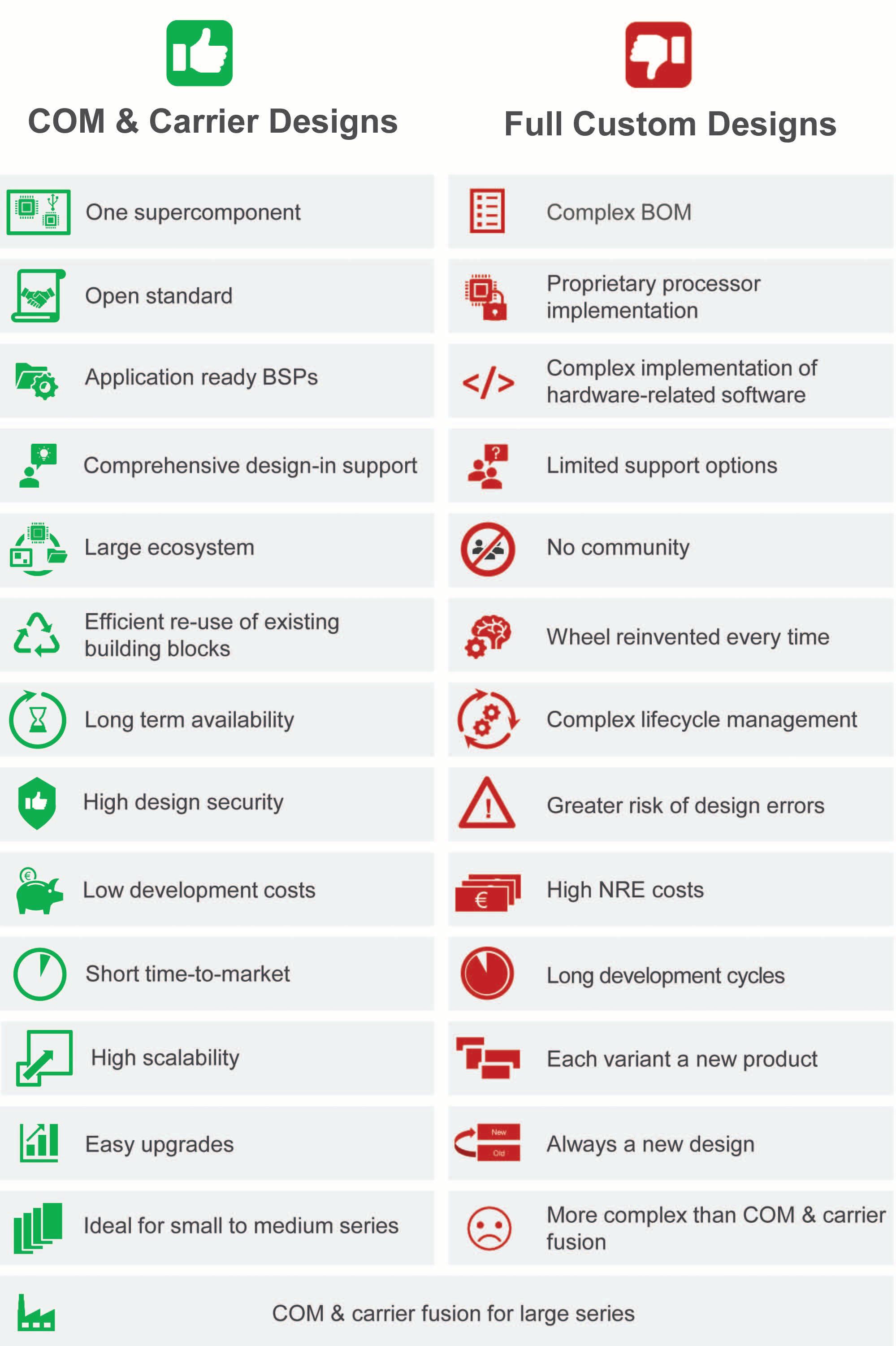

Edge Computing or Edge IoT is a recent development in the IoT market that is enjoying explosive growth in recent time. These terms refer to a recent development in distributed computing whereby computers, cameras and sensor processing systems are deployed in the same physical space where machines, robots and people connect and interact with the digital world.
Edge IoT is deployed when machine decision making needs to take place in real time and where there is a very high volume of on-site sensor data generated that is difficult to send to an off-site network (privacy regulation or connectivity issues for example). Some good examples of Edge IoT applications include warehouse order fulfilment, factory robotic systems, on-site retail, self-checkout and personal safety monitoring systems, train and airplane entertainment.
Analysts predict the Edge IoT market to be worth up to 155 billion USD by 2030 with Gartner forecasting up to 18 billion devices will deliver Edge IoT services by 2030. To meet the needs of such a diverse set of use cases presents a challenge for the semiconductor industry.
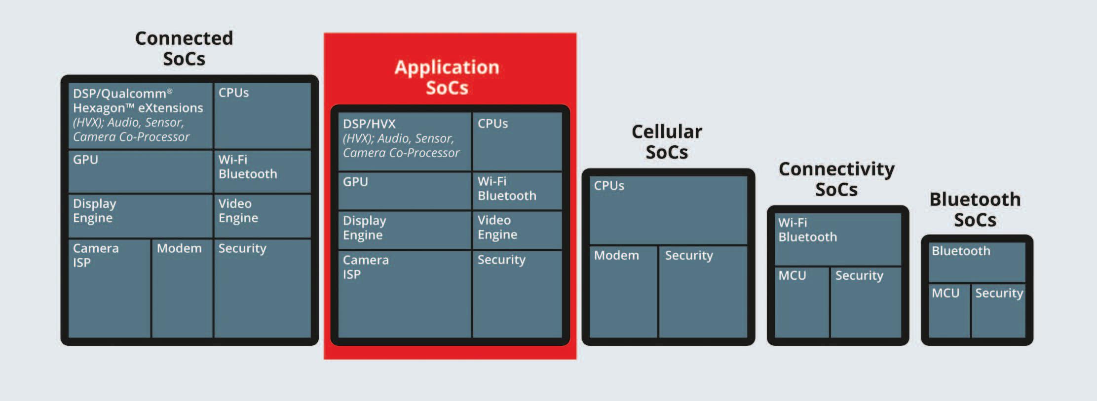
CODICO‘s long-time partner QUALCOMM has been busy in recent years developing SoC solutions that combine their technology strengths in computing and AI, camera,
wireless connectivity and audio to develop one of the most comprehensive roadmaps of SoC devices to support the many Edge IOT applications.

QUALCOMM SoCs for IoT are capable of powering all manner of devices, from low power IOT sensors to Voice UI capable headsets, handheld scanners, control panels, multi-camera and display automation, digital signage systems to robots, AGV’s and drones.

For each of these applications a highly integrated SoC solution is available to meet the power consumption, price and performance requirements. In this article we will take a closer look at the Application SoC roadmap for Edge IOT applications.
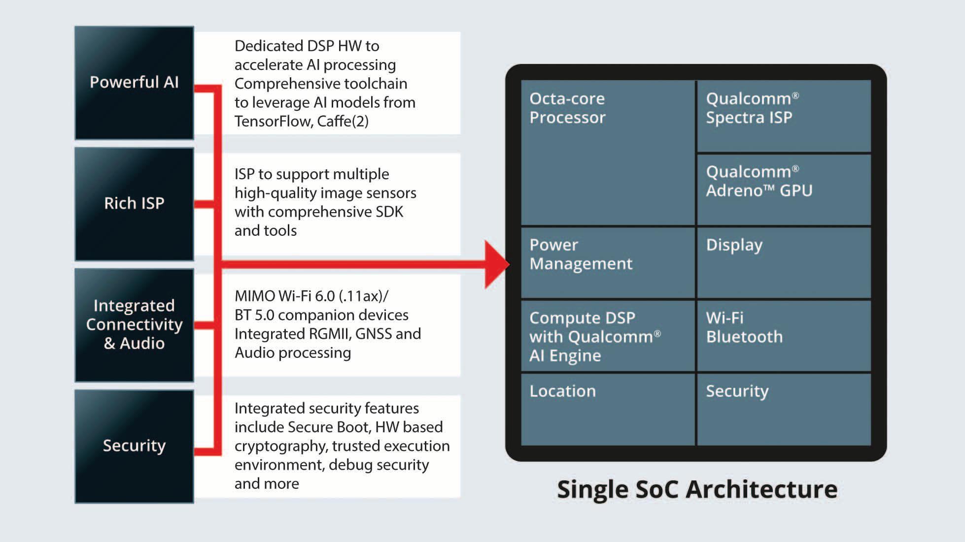
QUALCOMM’s range of Connected and Application SoCs offer a common architecture, the devices combine powerful compute and AI processing along with dedicated hardware blocks for camera, display, security and sensor processing. The highly integrated devices simplify hardware design complexity and provide for an optimised form factor.
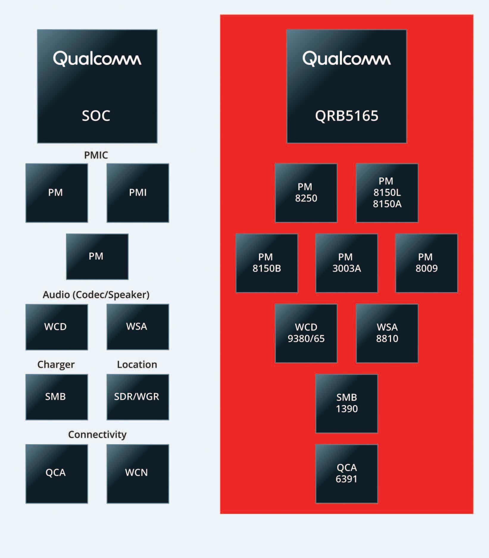
The current state of semiconductor supply presents designers and engineers with an unprecedented challenge as they try to identify semiconductor devices for their new products. QUALCOMM’s IoT roadmaps offers another advantage in this regard. The SoC devices are not provided as standalone devices, a portfolio of companion power management, audio CODECs, power amplifiers, charging, location and wireless connectivity solutions are available from QUALCOMM to accompany each of these SoC devices.
QUALCOMM’s Application SoC processors are tiered according to SoC performance, capabilities and pricing.
The matrix below captures a high-level overview of the key capabilities of each SoC available from QUALCOMM today. Entry level devices are optimised to meet a specific application for example the QCS405 for wireless audio or the QCS2290 for retail and industrial handheld devices. While SoCs in the higher tiers such as the QCS610 offer more capabilities and performance to allow designers to adopt the SoC for several use case such as Retail and Security cameras, Industrial Control Panels and Robotics.
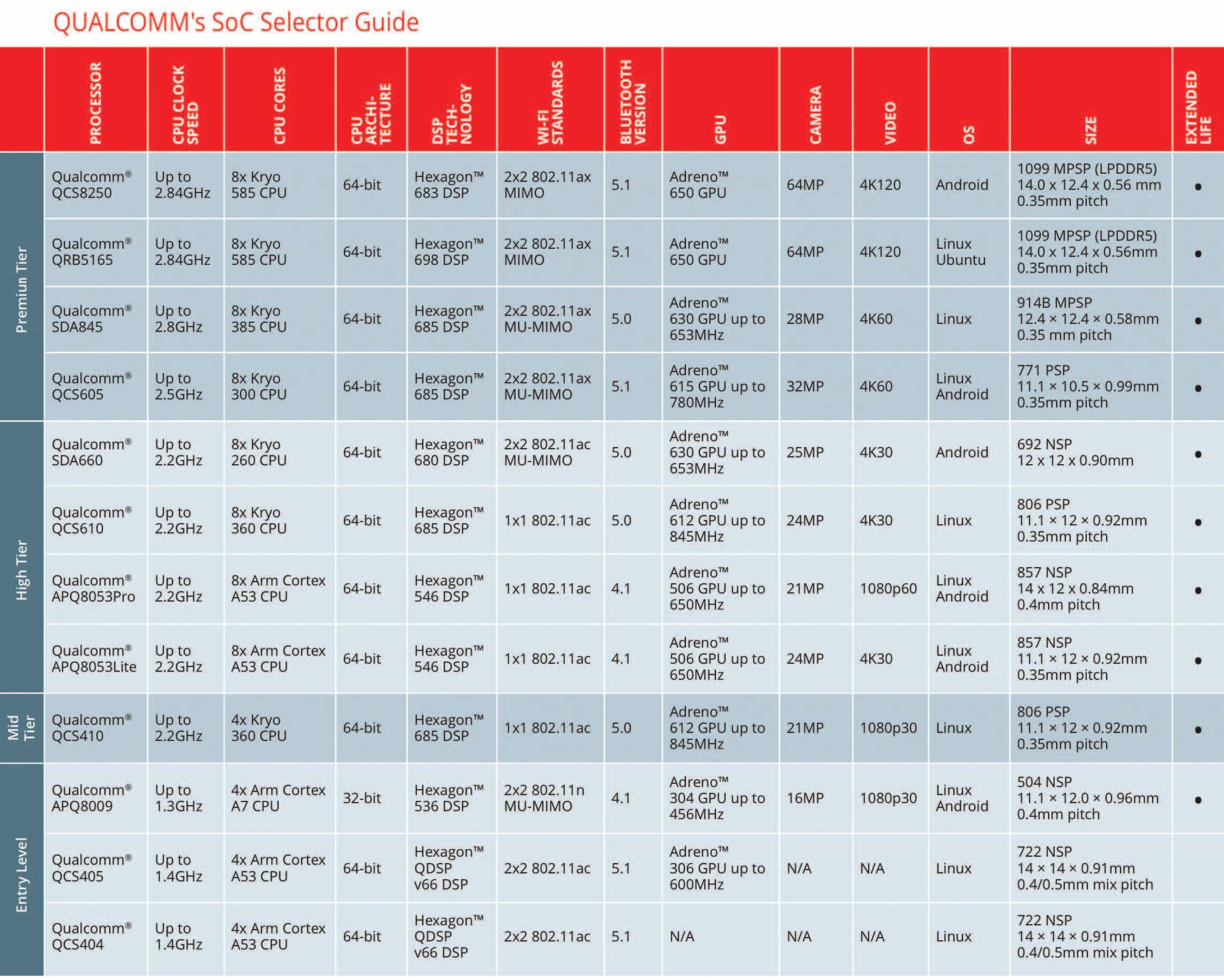
QUALCOMM’s SoC devices share a common architecture which enables designers to build a family of Edge IoT products using these devices which re-investing software components.
In some cases, pin for pin compatible devices such as the QCS2290/QCS4290 and QCS410/QCS610 are offered to meet the unique requirements of Smart Connected Camera and POS / handheld market segments.
Extended product lifetimes and extended temperature ranges are yet another requirement in the Edge IoT market which the QUALCOMM roadmap offers.
SoC product matrix taken from QUALCOMM’s Application-Processorsselector-guide_87-PN002-1-D which can be found here: https://www.qualcomm.com/content/da m/qcomm-martech/dm-assets/documents/application-processors-selectorguide_87-pn002-1-c.pdf
We expect the Edge IoT market to be a significant opportunity for our customers in the coming years.
Contact: Gabor Lefanti Field Sales Engineer Matroz Str. 4/b, 1213 Budapest, Hungary +43 1 86305-272

■ CODICO www.codico.com


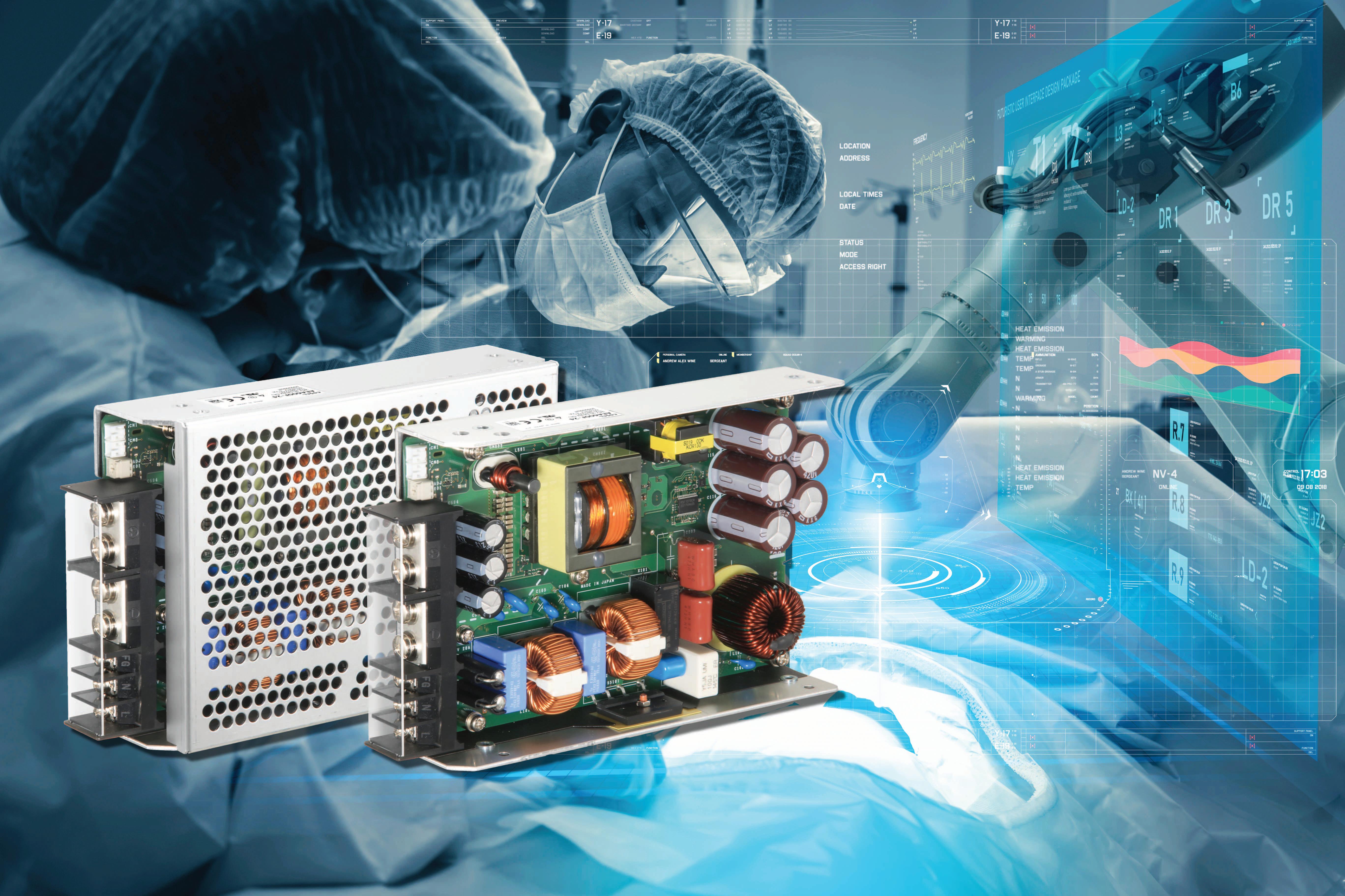
Power supplies are everywhere and there are no electronic equipments without one. Powered by battery or from the grid, there are as many power solutions as there are applications, and from body sensors powered by harvested energy to high power systems for medical imageries such as MRI, medical power supplies all have a common requirement to be safe, reliable and energy efficient. If a large majority of medical equipment requires conventional power supplies complying with their operating environment in effect running a marathon by delivering steady power day after day during their lifetime, then certain categories of applications require a power supply to deliver peak power, either occasionally or repetitively. For such applications medical equipment manufacturers must consider a number of parameters to make sure that the power supply they select will be able to not only run a marathon but in certain specific applications be able to perform a sprint race without compromising safety, performance and reliability.
Author: Patrick Le Fèvre Chief Marketing and Communication Officer Powerbox (PRBX)
What to consider when a marathon requires sprint race performance?
While it is granted for medical equipment manufacturers that a power supply must comply with safety standards (EN/IEC 60601-1), its output performance is very much dependent on the final equipment’s load behavior. If in monitoring and supervising systems the power consumption is relatively stable and easy to predict, in


medical equipment such as medicalized beds, infusion pumps, assisted patient ventilation including DC motors, and electromechanical-switches behaving as inductive or capacitive loads, then the power supply may have to deliver extra power for a period of few milliseconds to seconds (Figure 1). Though the duration time for peak power may be considered short compared to a normal operating time, it still
needs to be seriously considered to avoid costly surprises. Aside from the output voltage and power, the type of load will determine what is important for the system designer to consider. There are many possibilities and in some equipment the main power supply could power a variety of systems and sub-systems with different load profiles and that is obviously more complex to address. To simplify, we could list four basic types of loads: inductive, capacitive, constant current, and nonlinear resistive. All of them have a specific behavior requiring attention when selecting a power supply for each such application.
Inductive load: Loads such as motors and electromagnetic switches (e.g., relays, magnet switches) with an inductive characteristic are referred to as inductive loads. At the moment of applying a voltage to a DC-motor, a current multiple times the rated value will flow through the load; while at the moment of cutting the voltage off, due to the inductive component of the load a voltage of counter electromotive force E= -L× (di / dt) will be generated. Generally, when applying a voltage to an inductive load the power supply can sustain the energy required by the peak demand only up the limit of its overcurrent protection (OCP) function (Figure 2). Exceeding the limit, even if only for a very short time, can cause the power supply to stop. This is the reason why the peak load must be well defined in order to select an appropriate power supply with an overcurrent protection that allows the surge power for a definite time and sequence. Also, when turning the output voltage off, due to the counter electromotive force generated (in most cases, it is absorbed by the electrolytic capacitors in the power supply), the overvoltage protection circuit of the power supply may be triggered, and the power supply cease output. In this case measures such as including a reverse voltage protection diode should be exercised.
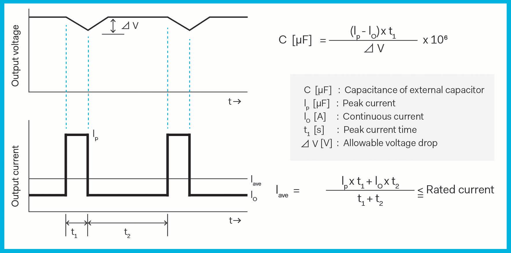
Capacitive load: A load with a capacitance component is called a capacitive load. For example, the capacitors inserted for the purpose of reducing the ripple voltage of the power supply, and capacitors used for coping with peak loads, etc. For this kind of load, at the moment of applying a voltage a very large charging current ipeak = (V/R) with R being the (parasitic) series resistance, will flow due to there being no charge in the capacitor. Although the power supply can detect and control the output voltage, if a large value capacitor (over several tens of thousands of microfarads) is inserted into the output side, such control may not be able to realize what is happening, and the output voltage may become unstable. It is important for system designers to consider the total amount of capacitance installed in their equipment and to verify the power supply’s ability to deliver the required peak energy needed to efficiently charge the load which in some applications could be several Farads.
Figure 2: Typical overcurrent protection curves.
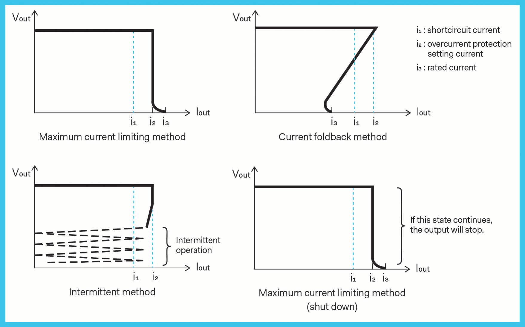
Figure 3: Peak current at startup when charging capacitors.
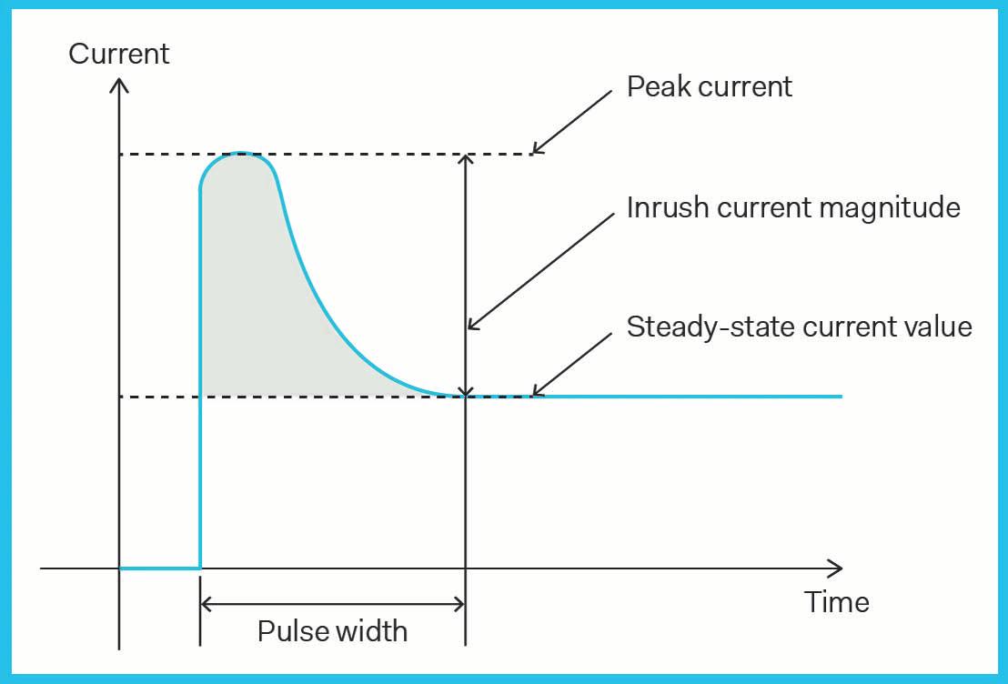
Figure 4: Design equation to guarantee output capacitors to sustain required peak energy
Constant current load: A load where the current stays constant although the load voltage varies is called a constant current load, an example being LED lighting in surgical theaters. It is important to consider the type of overcurrent protection built into the power supply. If for example the overcurrent protection characteristic of the power supply is a current fold back type, the output voltage may not be able to rise (Figure 2). This is because the output voltage stabilizes on the drooping line of the
short time, for the power supply it may look like a constant current exceeding the threshold value for its built-in overcurrent protection.
In the previous short descriptions overcurrent protection has been mentioned, this being a very important part of a power supply. It guarantees the power unit in the case of an excess power situation that may occur accidentally or as result of an equipment failure, to protect the equipment and eventually flag up the
Depending on the type of application and specific system requirements, when OCP is activated a number of effects may result, the output could be switched off permanently with a manual reset, switched off temporarily with an automatic reset, or behave as a fixed, but safe level constant current (Figure 2).
When a power supply or an electrical device is turned on, high initial current flows into the load, starting at zero and ramping up until it reaches a peak value.
overcurrent protection characteristic of the power supply from applying a voltage to reaching the rated voltage. Generally, by changing the overcurrent protection characteristic to a maximum current limiting type the problem can be solved.
Non Linear Resistive: Some equipment uses heating elements or lamps with filaments where the resistance changes when current flows through it. Though this warm up phase with a monotonic resistance change might only last for a
fault by way of a signal to the operator, e.g. a LED or a signal transmitted by the communication BUS.
As previously explained, when the output current/power exceeds a defined limit, several types of damage could occur within the power supply or in the equipment being powered. Besides preventing the current from exceeding a rated value, the protection circuit also plays the role of limiting short circuit current.
The main reason for this initial peak is to charge the large decoupling or smoothing capacitors within the power supply and final equipment. During this sequence, as the capacitors charge or devices come out of a cold state, the current increases very fast from zero, rising all the way to the peak current and then decreasing gradually to the steady state current (Figure 3). During this period the power supply must deliver enough energy to charge the capacitors, and supply the required power to the load without activating the over-current protection
©
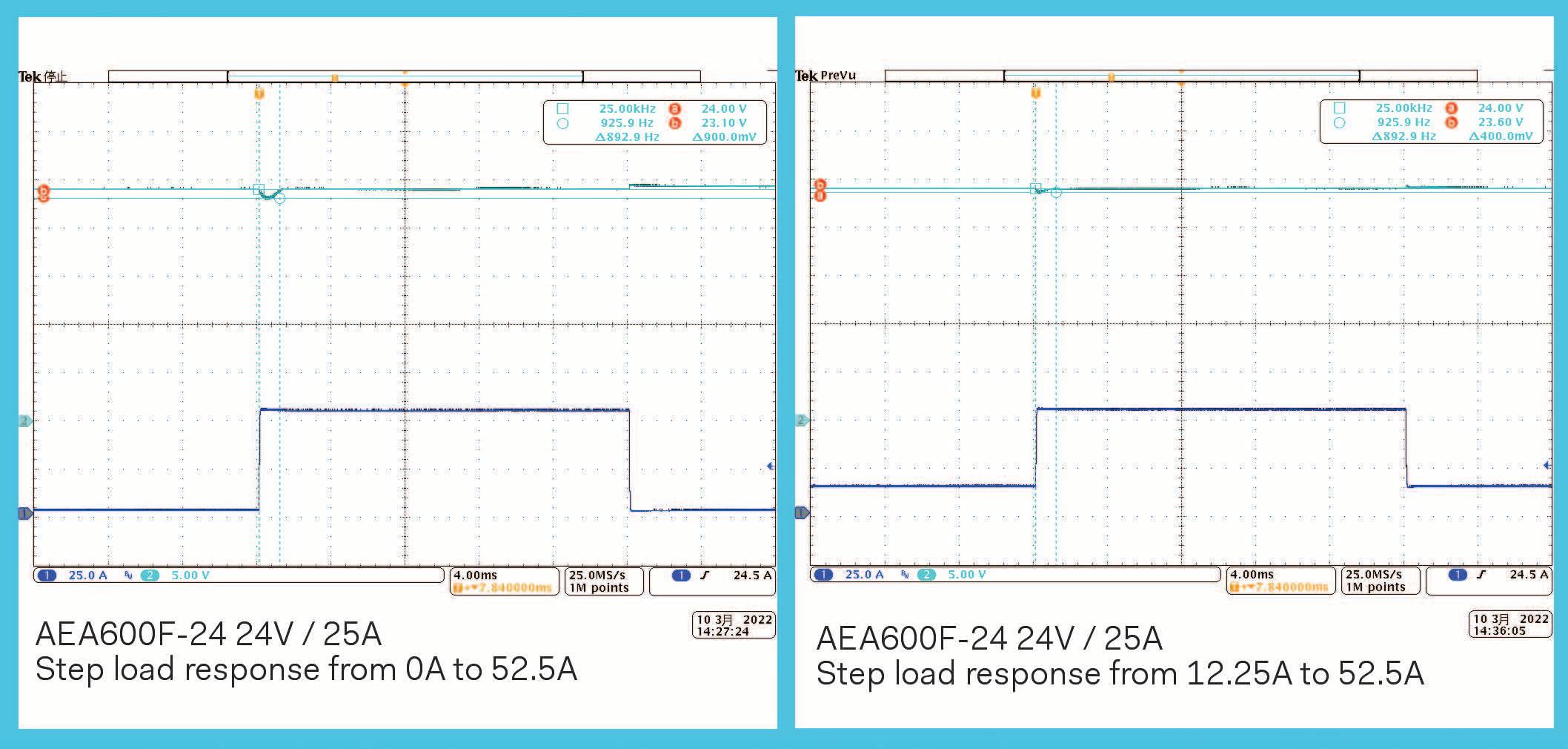
Figure 6: COSEL AEA600F peak load test in two conditions (0 to 200% and 50% to 200% load).
(OCP) thus shutting down the output. Also, some loads might initially behave as a short-circuit and require the power supply not to go into protection mode. To accommodate this start-up sequence, power supplies are designed to allow a certain level of overcurrent, and it is common to set the OCP threshold at around 110% of the maximum rated value.
110% is good enough for the vast majority of applications though in the case of demanding medical equipment requiring peak power levels in the range of 200300% for seconds, then 110% will not work and it requires a power supply designed not only to deliver a high peak power, but to guarantee the highest reliability during the overall lifetime of the final equipment.
Running a marathon at sprint performance levels! A simple way to secure the power supply to deliver enough energy when extra surge power is required is to choose a power unit rated for the maximum power required during the peak demand. For example if the maximum steady power required by an apparatus is 500W and the peak is 1000W, then taking into consideration the operating conditions e.g., input voltage, environmental temperature, derating, etc., the system designer could con-
References
• Powerbox (PRBX): https://www.prbx.com
• COSEL: https://en.cosel.co.jp
sider a 1200W power supply as the most suitable solution. This seems to be obvious yet overkill when the peak is only happening occasionally. For example when a DC motor is activated for positioning a patient’s bed then switched off and the power supply is only powering the control system. Similarly overkill for systems requiring repetitive peak loads for a limited time compared to steady state power. Choosing a power supply for peak load applications requires one to evaluate the operating conditions during the lifetime of the equipment, and to take into consideration all aspects including size, weight and price. Buying a 1200W power supply when a peak load representing a limited portion of the operation might not be the best option.
Power supply manufacturers have developed power solutions able to deliver significant extra power in the region of twice nominal, or even more than the maximum rated, for a significant duration. This requires the power unit to be designed to host enough capacitors (Figure 4) but also to have a power-train able to sustain repetitive peak demands without over-heating or adversely affecting reliability.
As an example, we could have a quick look at the output voltage behavior of the COSEL 600W AEA600F series (Figure 5) when
applying a peak load to the output. The tested product is a 600W rated power unit, delivering 24V at a nominal current of 25A. As presented in Figure 06, the power-train and output capacitors have been selected to sustain a peak power twice nominal for a duration of 1000 milliseconds. Two conditions are represented in Figure 6: From no load to 52.5A peak, and from 12.25A half-load to 52.5A peak. In both conditions, the voltage remains within the specified limits, and OCP is not shutting down the output.
Running a marathon with sprint-race performance levels in medical power supplies is a reality, and while the great variety of applications require different types of power supplies, technology is making it easier for system designers to choose the right products for their applications. This is without mentioning the fantastic opportunities brought about by new technologies such as Wide Band Gap semiconductors, Supercapacitors, and digital control coming to the next generation of power supplies, and making power designers’ lives so exciting.
■ Powerbox (PRBX) www.prbx.com
In recent years, there has been an explosive demand for high-resolution, bandwidth-hungry imaging technologies that integrate Artificial Intelligence (AI) with an increased focus on real-time analytics and edge computing. Edge computing, unlike centralized cloud computing, is a distributed computing paradigm that improves response times and saves bandwidth by making compute resources available close to the data sources. With the ever-burgeoning Internet of Things (IoT), an increasing number of commercial and industrial applications are relying on an interconnected web of sensor-based, digital and mechanical machines to monitor and control tasks. At the core of the IoT are wireless-enabled embedded systems, real-time analytics and machine learning inference.

These systems evidently constitute two core elements – a computing system and a transport mechanism. Challenges in designing such systems include efficient accelerated performance with predictable outcomes plus a flexible, error-free serial link that supports high data rates and are scalable. However, the most significant design constraints for an edge computing device are power and size - some of these devices
could be deployed in remote locations or might require an uninterrupted power supply for critical applications while conforming to strict form-factor requirements such as in automotive vision systems, military surveillance, medical equipment, high-precision industrial tools and more.
Microchip’s Comprehensive Solution

Fully cognizant of the need for intelligent vision systems and their associated challenges, Microchip have developed the lowest power, smallest form factor, costoptimized solution for all your multiGigabit, uncompressed, video and data needs. The solution integrates our PolarFire Field-Programmable Gate Arrays (FPGAs) with our CoaXPress 2.0 transceivers to enable high-speed serial transmission of imaging data from multiple cameras to the FPGA for image signal processing. Microchip offer a complete reference design: PolarFire CoaXPress 12G Design, that includes evaluation hardware, intellectual property and user documentation to accelerate your development time.
The PolarFire CoaXPress 12G Design employs dual 4K camera sensors connected to a PolarFire MPF100T FPGA over the MIPI CSI-2 protocol. The FPGA performs an
8b/10b encoding operation and re-organizes the incoming stream into data packets defined by the CoaXPress protocol. This signal is transmitted by an onboard EQC125X40 CoaXPress transceiver, over a 50m coaxial cable to another EQC125X40 transceiver that reconstructs the transmitted signal from the attenuated high-speed received signal. This board is connected to a PolarFire video kit, MPF300-VIDEO-KITNS, over an FPGA Mezzanine Card (FMC) [BTC1] connector; where a PolarFire device with 300,000 Logic Elements (LE) carries out the 8b/10b decoding followed by any desired image processing or intelligent algorithmic processing. Amongst a host of other interfaces, the board also supports an HDMI output to display the received signal on a screen. So, designers have an end-to-end demonstration of an embedded vision system.
The total power drawn by the above design is < 1W - the lowest power available on the market. Additionally, with the PolarFire FPGA offered in form factors as small as 11 ×11 mm and the CoaXPress 2.0 transmitter/receiver/repeater offered in a tiny 4 × 4 mm package, the design is dramatically optimized for both power and size! This solution is well suited for creating nextgeneration embedded vision platforms that integrate AI and Machine Learning (ML).
PolarFire FPGAs deliver the industry’s lowest power in mid-range densities and provides defense-grade security and exceptional reliability. The product family spans from 100K to 500K LEs, features 12.7 Gigabit-per-second (Gbps) transceivers, a robust DSP and high-speed memory resources. PolarFire FPGAs are great options for any design that requires high-bandwidth video signals and power over coaxial cables. PolarFire FPGAs are flexible solutions that provide a suite of image processing IP to support popular imaging and video protocols including MIPI CSI-2 TX, MIPI CSI-2 RX, HDMI 1.4 TX, HDMI 2.0, DSI, and HD/3G/6G/12G SDI.
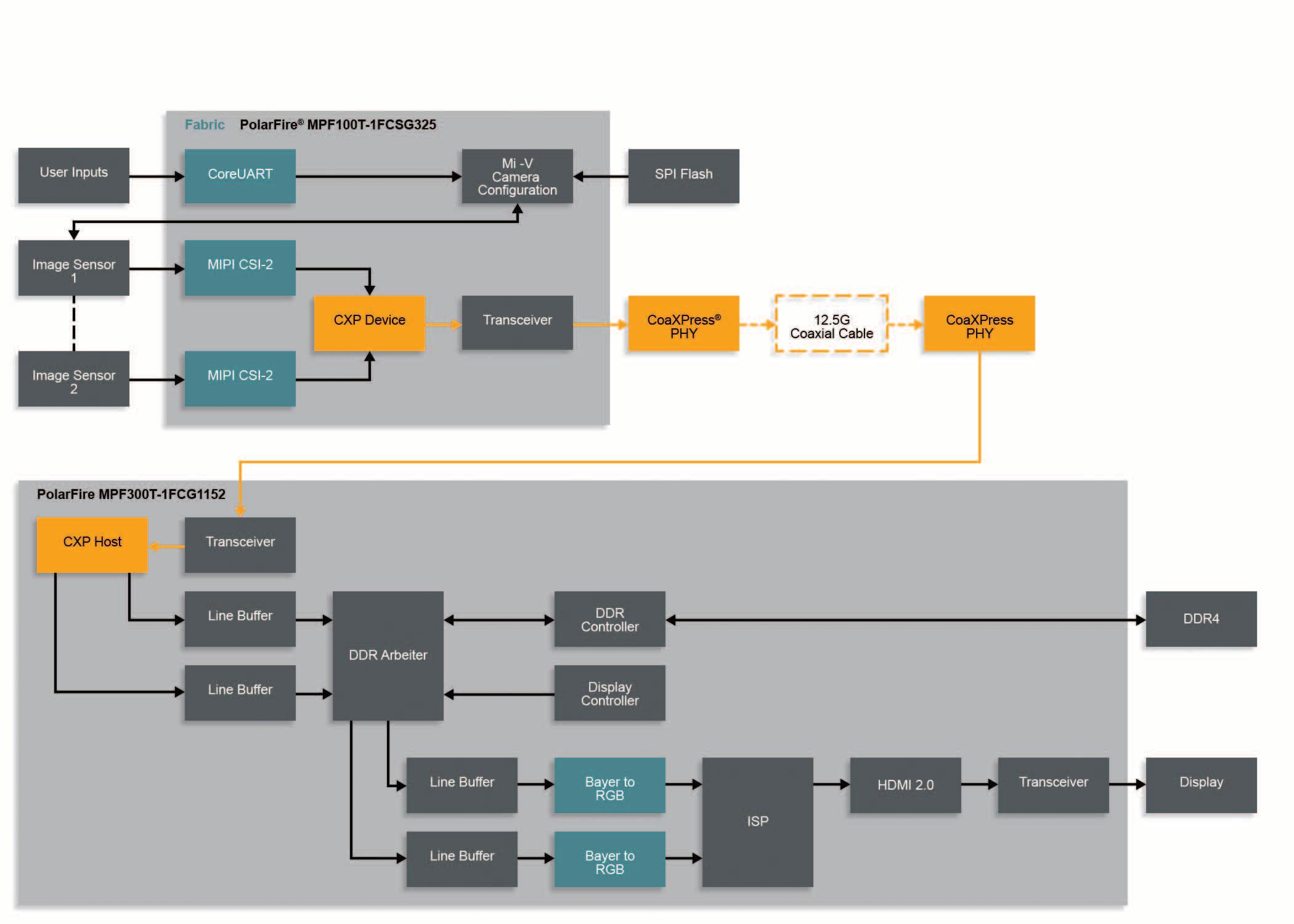
CoaXPress technology is an open and royalty-free asymmetric, high-speed, pointto-point open serial communication standard for high-performance machine vision, industrial inspection and traffic monitoring systems. It provides a state-ofthe-art method for connecting high-performance, high-resolution cameras to high-speed capture cards – which are also known as frame grabbers – via standard, off-the-shelf 75Ω coaxial cables.
Offering a significant improvement in speed over CoaXPress v 1.1, CoaXPress 2.0 extends the data transfer rate up to 12.5 Gbps for cables lengths of up to 40m, and
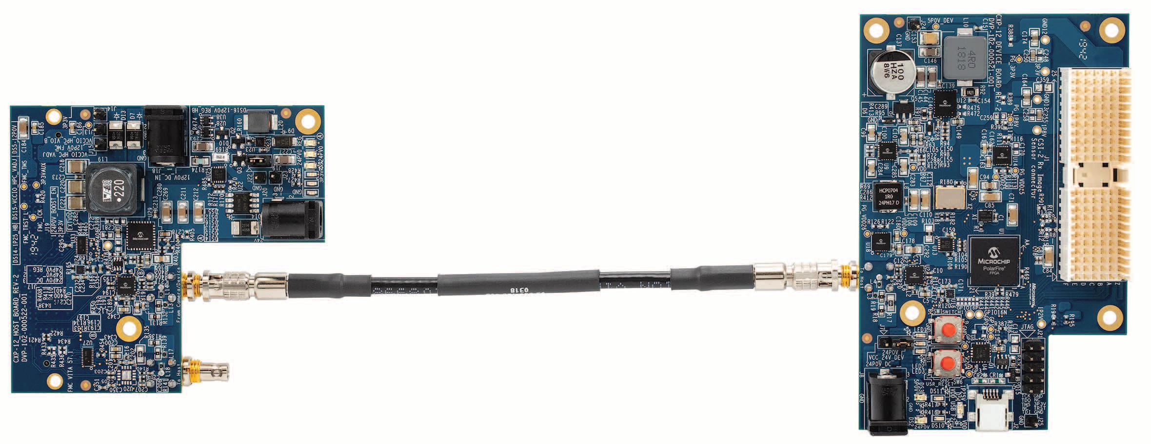
up to 40 Megabits per second (Mbps) for bidirectional communications. It is in fact, the only 12.5 Gbps standard that provides simultaneous video, camera control, and triggering over a single coaxial cable, along with 13W of DC power at 24 VDC, with real-time cable link quality check.
■ Microchip Technology www.microchip.com

Mouser Electronics, Inc., the industry’s leading New Product Introduction (NPI) distributor with the widest selection of semiconductors and electronic components, today announced the launch of a new resource site dedicated to sensor design guides. The resource site features a growing collection of articles dedicated to the intricacies of sensor design applications, providing engineers with the information they need to solve complicated design challenges. Readers can access the resource site by visiting https://resources.mouser.com/sensordesign-guides/.
Advances in sensor design have supported innovative new devices in consumer electronics, medical applications, and automotive manufacturing. The new sensor design guide resource site offers a range of rich, indepth articles on topics including time-offlight sensors, MEMS microphones, gyroscopes, and accelerometers.
In an article on board-mounted temperature sensors, embedded systems expert Ishmael Chigumira explores the technological innovations that have made it possible for temperature sensors to be integrated in a PCB instead of located off-board. The article defines the different types of temperature sensors, explains how to interpret boardmounted sensors, and prescribes several best practices for integration and implementation. In The Dos and Don’t of VOC Sensors, electronic engineer Robin Mitchell provides a detailed introduction to the different types of sensors used to measure volatile organic compounds (VOCs). The article also explores the various applications for VOC sensors and offers tips on how to choose the right solution for each potential design.
To begin learning more about sensor design, visit https://resources.mouser.com/sensordesign-guides/.

■ Mouser Electronics https://www.mouser.com
Mouser Electronics, Inc. announces a new eBook in collaboration with Analog Devices, Inc. exploring the latest innovations in power management and how they can be used in a range of applications. The eBook, titled Power Management for All of Tomorrow’s Innovations, examines new technology developments for cutting-edge applications, including electric vehicles, asset tracking, wearables, and Internet of Things (IoT) devices.
Today’s original equipment manufacturers face a complicated challenge when it comes to power management: An effective design must deliver stable performance while maintaining low power emissions and affordability. From demanding applications like vehicle batteries to the next generation of medical devices and consumer electronics, power management is a vital consideration for the design and manufacture of cutting-edge solutions. The new eBook features a range of articles, infographics, and instructional videos, providing rich context on the use of Analog Devices products in power management applications.
The Power Management for all of Tomorrow’s Innovations eBook offers direct links to eight relevant products from Analog Devices, connecting engineers directly to solutions for innovative power management applications. Featured products include the LT8316 micropower isolated flyback converters, a highly efficient solution that reduces transformer size and improves load regulation. The LT8316 converters support a range of applications, including electric vehicles, isolated off-line housekeeping power supplies, and isolated telecom, industrial, and medical power supplies.
The LTC2971 two-channel power system managers are capable of sequencing, trimming, margining, supervising, managing, logging faults, and monitoring telemetry across two power supplies. Featuring a proprietary soft-connect algorithm to minimise supply disturbances, the LTC2971 power system managers offer reliable performance for computer and network servers, industrial test and measurement, and video and medical imaging.
To read the new eBook, go to https://www.mouser.com/ebooks/PowerManagement-for-all-of-Tomorrows-Innovations.

■ Mouser Electronics https://www.mouser.com

Alain Bruno Kamwa, Corporate Product
SalesManager Opto at Rutronik Elektronische Bauelemente GmbH, explains below which light beams are suitable for the technologies of the city of the future. As progress, efficiency, safety, ecology and inclusion are the crucial aspects that are in focus when implementing a smart city vision.

You cannot do without light – light is energy, brightness and color. It is everywhere, (in)visible and perceptible. Light is a form of electromagnetic radiation that has a constant influence on people, flora and fauna – and on technologies. The different wavelengths of this radiation are used in a variety of established, as well as cuttingedge, applications.
Since the end of the 20th century, it was impossible to imagine medical diagnostics without short-wave X-rays. The particularly long-wavelength radio ensures the wireless transmission of data. With advancing technologies, UV, infrared (IR) and artificially generated laser radiation are also gaining new fields of application.
The latter – especially as LiDAR (light detection and ranging) – and IR are gaining additional importance in the realization of smart living concepts.
The knowledge of how humans, animals and nature are influenced by different lighting scenarios is already being used in shopping centers, production facilities and agriculture. Lighting similar to daylight, for example, ensures greater concentration and safety in the workplace and is also established in retail, as colors and color differences are easy to recognize with a color temperature of 6,000 Kelvin, a bright, clear and radiant white. A “warmer” lighting concept with 2,700 Kelvin, on the other hand, is more conducive to relaxation and calm.
The combination of sensor technology and lighting enables comprehensive lighting concepts that combine various tasks. Here, energy-efficient and long-lasting
LEDs take over the illumination of indoor and outdoor areas. The light sources can be controlled almost in real time to adapt intensity and color to the respective situation. This significantly increases safety in both private and public spaces, while being much more energy-efficient than permanent lighting. In addition, special emitting UV LEDs make the urban farming concept a reality for almost any city. Especially in outdoor areas, this could be supplemented by energy harvesting technologies: Here, floor plates convert friction caused by footsteps or movement into energy that can be used to power integrated sensor systems.
The integration of high-power infrared LEDs, such as those from ams OSRAM's OSLON® P1616 product range, extends
the smart city security concept, for example as night vision cameras, 2D face recognition for user authentication and intelligent doorbells. Due to their small size of 1.6 mm × 1.6 mm, the products are perfect for all space-critical applications while maintaining high optical performance, efficiency and reliability. Due to the wide temperature range from -40 to +105°C, they are suitable for a wide range of applications. This product range is also suitable for the realization of eyetracking applications, which, for example, enable people with a physical impairment to participate more actively and independently in social life again. The IR technology is used primarily to detect fixations (eyes remain fixed on a point for a long time) and saccades (eyes move quickly) and to execute commands based on these. One application scenario, for example, would be menu navigation on smartphones, computers and vending machines, but also the opening of doors and the use of checkout systems.

This does not just mean the production of vitamin D, which is important for the human body. With infrared (IR) sensors integrated in mobile devices, such as the ams OSRAM BIOFY® series, it is possible to check the freshness of food at any time –using IR spectroscopy. Spoiled stomachs can thus be easily avoided in the future. This technology is already being used successfully in the food industry and thus also offers a reliable solution for counteracting food waste. ams OSRAM offers the P1616 SFH4737 broadband emitter for this purpose with a spectral emission range of 650 nm to 1050 nm, a particularly small design (1.6 mm × 1.6 mm × 0.9 mm) and an emission angle of 130°, which means that light can be absorbed within a larger area. The broad homogeneous spectrum of the wavelength range enables a wide coverage of infrared light sources.
Biomonitoring sensors also make it possible to monitor blood oxygen levels and heart rate without interruption. Especially in the care of people in need of care, this means a bit more freedom for those affected, because handy and, above all, significantly smaller devices replace the bulky, medical monitoring devices. A discreet smartwatch does not disturb the wearer in everyday life, but provides the necessary security: If the sensor registers irregularities, an emergency call can be made immediately. It is also possible to detect medication by means of IR spectroscopy, an advantage for caregivers. This is an advantage for caregivers, because senior citizens living alone are often confused when taking medication, which can lead to dangerous interactions. If the watch also has an acceleration sensor that can detect a fall and a GNSS positioning function, the nearest emergency services are alerted and receive a very accurate emergency scenario, which saves a considerable amount of time.
Mobility concepts for a smart city require reliable and precise technologies to prevent accidents, ensure the safety of people and animals, and create optimum efficiency. LiDAR, for example, is used to measure distances around vehicles and thus the distance to potential obstacles. In LiDAR sensors, a pulsed IR laser diode emits a light pulse. If this is reflected by an obstacle, the sensor detects it.
The distance between the sensor and the obstacle can be determined from the time between the emission and arrival of the light waves, the time of flight (ToF). A ToF camera can help increase driving safety in the interior of a vehicle, for example by monitoring the driver, passengers and objects in the passenger compartment.
Then the system can detect when the driver is distracted or tired before an accident occurs. Interior monitoring also makes it possible to detect head and body positions, for example for optimal
airbag alignment; it can also be used to control controls by gesture. Outside the vehicle, a ToF solution can support assisted and autonomous driving. Melexis has developed a demo kit for IR lighting in ToF applications specifically for in-car interior monitoring.
The demo board features high on-board processing for hand gesture recognition and high image resolution for object classification. This makes it suitable not only for gesture recognition and for driver monitoring, but also for skeleton
tracking, person and obstacle detection, and traffic monitoring.
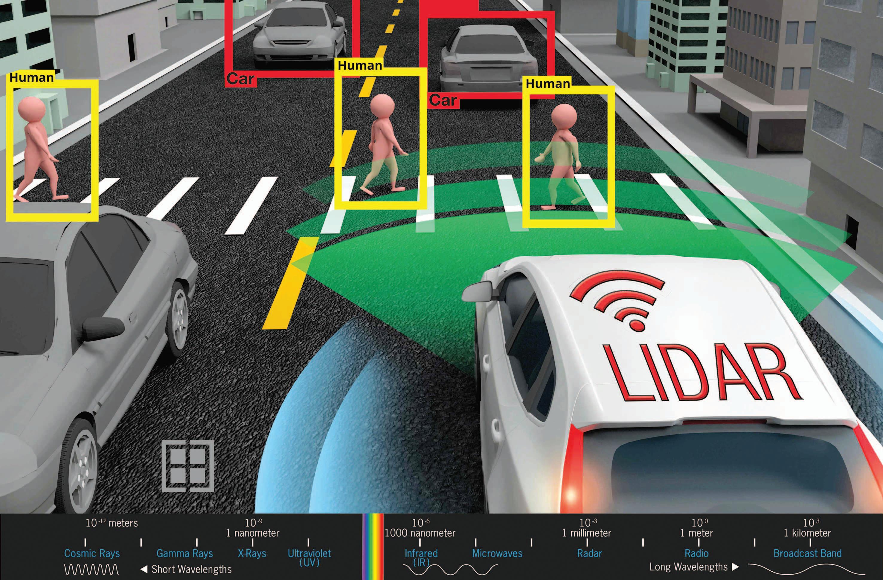
The demo board is equipped with a VCSEL (Verical Cavity Surface Emitting Laser) from Lextar's PV85Q series. It features high efficiency and a narrow spectral bandwidth (1.8 nm). Its various optical power options enable multiple object detection, 3D depth assistance and presence detection. For eye safety, the VCSEL includes a photodiode. The fully integrated MLX75027 VGA (640 × 480) optical ToF image sensor comes with 10 × 10 μm DepthSense® pixels.
Not all light is the same
Thanks to an extensive LED manufacturer portfolio, Rutronik offers the optimum solution for a wide range of requirements. The associated technologies for thermal management, for example, and of course sensor technology can also be provided from a single source. Rutronik's interdisciplinary experts thus have a deeper understanding of a complex overall system. They advise and accompany the implementation of an individually suitable solution for the realization of smart city, smart and urban farming concepts.

■ Rutronik www.rutronik.com
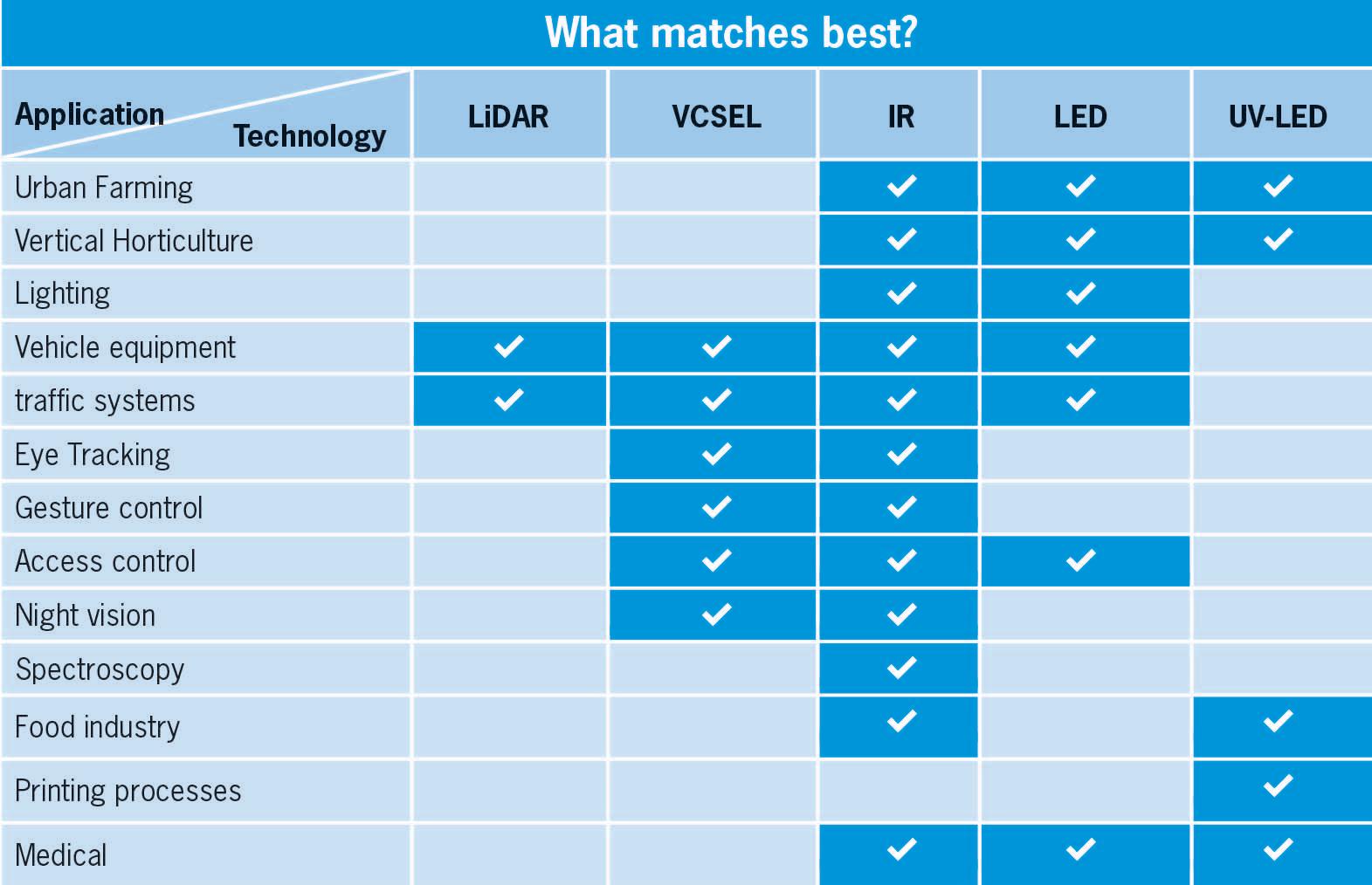


Renesas Electronics Corporation and Fixstars Corporation, a global leader in multi-core CPU/GPU/FPGA acceleration technology, announced the joint development of a suite of tools that allows optimization and fast simulation of software for autonomous driving (AD) systems and advanced driver-assistance systems (ADAS) specifically designed for the R-Car system-on-chip (SoC) devices from Renesas. These tools make it possible to rapidly develop network models with highly accurate object recognition from the initial stage of software development that take advantage of the performance of the R-Car. This reduces post-development rework and thereby helps shorten development cycles.
“Renesas continues to create integrated development environments that enable customers to adopt the “software-first” approach,” said Hirofumi Kawaguchi, Vice President of the Automotive Software Development Division at Renesas. “By supporting the development of deep learning models tailored to R-Car, we help our customers build AD and ADAS solutions, while also reducing the time to market and development costs.”
“The GENESIS for R-Car, which is a cloudbased evaluation environment that we built jointly with Renesas, allows engineers to evaluate and select devices earlier in the development cycles and has already been
used by many customers,” said Satoshi Miki, CEO of Fixstars. “We will continue to develop new technologies to accelerate machine learning operations (MLOps) that can be used to maintain the latest versions of software in automotive applications.”
Today’s AD and ADAS applications use deep learning to achieve highly accurate object recognition. Deep learning inference processing requires massive amounts of data calculations and memory capacity. The models and executable programs on automotive applications must be optimized for an automotive SoC, since real-time processing with limited arithmetic units and memory resources can be a challenging task. In addition, the process from software evaluation to verification must be accelerated and updates need to be applied repeatedly to improve the accuracy and performance. Renesas and Fixstars have developed the following tools designed to meet these needs.
1 R-Car Neural Architecture Search (NAS) tool for generating network models optimized for R-Car
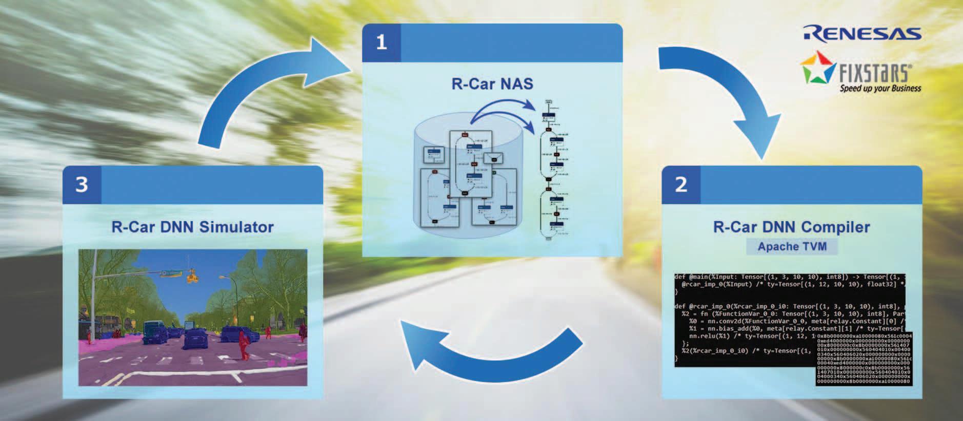
This tool generates deep learning network models that efficiently utilize the CNN (convolutional neural network) accelerator, DSP, and memory on the RCar device. This allows engineers to rapidly develop lightweight network models that achieve highly accurate object
recognition and fast processing time even without a deep knowledge or experience with the R-Car architecture.
2 R-Car DNN Compiler for compiling network models for R-Car
This compiler converts optimized network models into programs that can make full use of the performance potential of R-Car. It converts network models into programs that can run quickly on the CNN IP and also performs memory optimization to enable high-speed, limited-capacity SRAM to maximize its performance.
3 R-Car DNN Simulator for fast simulation of compiled programs
This simulator can be used to rapidly verify the operation of programs on a PC, rather than on the actual R-Car chip. Using this tool, developers can generate the same operation results that would be produced by R-Car. If the recognition accuracy of inference processing is impacted during the process of making models more lightweight and optimizing programs, engineers can provide immediate feedback to model development, therefore shortening development cycles.
For more information, please visit: https://www.renesas.com/software-tool/toolsoptimize-ai-software-adadas-r-car-soc
Renesas Electronics https://www.renesas.com
Ambarella, Inc., an edge AI semiconductor company, today announced the world’s first centralized 4D imaging radar architecture, which allows both central processing of raw radar data and deep, low-level fusion with other sensor inputs—including cameras, lidar and ultrasonics. This breakthrough architecture provides greater environmental perception and safer path planning in AI-based ADAS and L2+ to L5 autonomous driving systems, as well as autonomous robotics. It features Ambarella’s Oculii™ radar technology, including the only AI software algorithms that dynamically adapt radar waveforms to the surrounding environment—providing high angular resolution of 0.5 degrees, an ultra-dense point cloud up to 10s of
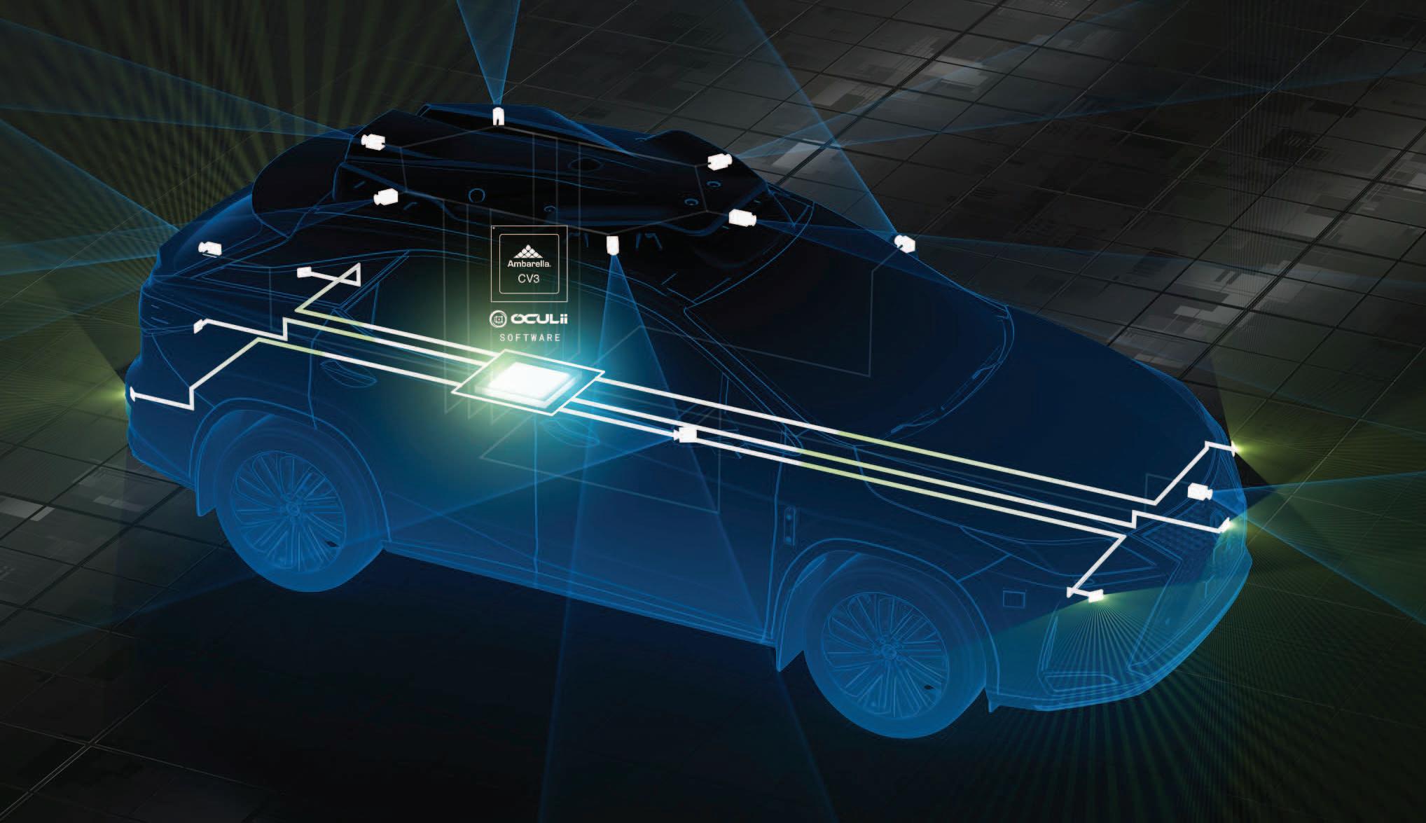
thousands of points per frame and a long detection range up to 500+ meters. All of this is achieved with an order of magnitude fewer antenna MIMO channels, which reduces the data bandwidth and achieves significantly lower power consumption than competing 4D imaging radars. Ambarella’s centralized 4D imaging radar with Oculii technology provides a flexible and high performance perception architecture that enables system integrators to future proof their radar designs.
To create this unique, cost-effective new architecture, Ambarella optimized the Oculii algorithms for its CV3 AI domain controller SoC family and added specific radar signal processing acceleration. The
CV3’s industry-leading AI performance per watt offers the high compute and memory capacity needed to achieve high radar density, range and sensitivity. Additionally, a single CV3 can efficiently provide high-performance, real-time processing for perception, low-level sensor fusion and path planning, centrally and simultaneously, within autonomous vehicles and robots.
“No other semiconductor and software company has advanced in-house capabilities for both radar and camera technologies, as well as AI processing,” said Fermi Wang, President and CEO of Ambarella. “This expertise allowed us to create an unprecedented centralized architecture
that combines our unique Oculii radar algorithms with the CV3’s industry-leading domain control performance per watt to efficiently enable new levels of AI perception, sensor fusion and path planning that will help realize the full potential of ADAS, autonomous driving and robotics.”
The data sets of competing 4D imaging radar technologies are too large to transport and process centrally. They generate multiple terabits per second of data per module, while consuming more than 20 watts of power per radar module, due to thousands of MIMO antennas used by each module to provide the high angular resolution required for 4D imaging radar. That is multiplied across the six or more radar modules required to cover a vehicle, making central processing impractical for other radar technologies, which must process radar data across thousands of antennas.
By applying AI software to dynamically adapt the radar waveforms generated with existing monolithic microwave integrated circuit (MMIC) devices, and using AI sparsification to create virtual antennas, Oculii technology reduces the antenna array for each processor-less MMIC radar head in this new architecture to 6 transmit x 8 receive. Overall, the number of MMICs is drastically reduced, while achieving an extremely high 0.5 degrees of joint azimuth and elevation angular resolution. Additionally, Ambarella’s centralized architecture consumes significantly less power, at the maximum duty cycle, and reduces the bandwidth for data transport by 6x, while eliminating the need for pre-filtered, edge processing and its resulting loss in sensor information.
This cost-effective, software-defined centralized architecture also enables dynamic allocation of the CV3’s processing resources, based on real-time conditions, both between sensor types and among sensors of the same type.
For example, in extreme rainy conditions that diminish long-range camera data, the CV3 can shift some of its resources to improve radar inputs. Likewise, if it is raining while driving on a highway, the CV3 can focus on data coming from frontfacing radar sensors to further extend the vehicle’s detection range while providing faster reaction times.
This can’t be done with an edge-based architecture, where the radar data is being processed at each module, and where processing capacity is specified for worst-case scenarios and often goes underutilized.
These two different approaches to radar processing are summarized in the following table:
These radar heads eliminate the need for a processor, which reduces costs for both the upfront bill of materials and in the event of damage from an accident (most radars are located behind the vehicle’s bumper). Additionally, many of the edge-processor radar modules deployed today never receive software updates because of this software complexity.
Competing Edge-Processed Radar Ambarella’s Centralized Radar Processing
Constant, repeated radar waveforms
Oculii™ AI software algorithms dynamically without regard for environmental adapt radar waveforms to surrounding conditions environment
MMIC + edge radar processor in module MMIC only in “radar head”
Radar detection processing in radar Radar detection processing in central processor module
Multiple terabits per second, per 6x bandwidth reduction for radar data transport module of radar data (too large to transport and process centrally)
1+ to 2° resolution 0.5°of joint azimuth and elevation angular resolution
High power consumption, due to Low power consumption, due to order of 1000s of antenna MIMO channels magnitude fewer antenna MIMO channels used by each radar module (6 transmit x 8 receive antennas in each processor-less MMIC radar head)
No dynamic processing allocation Dynamic allocation of CV3’s processing (specified for worst-case scenarios) resources, based on real-time conditions, between sensor types and among sensors of same type
Slow processing speeds CV3 is up to 100x faster than traditional edge radar processors
CV3 marks the debut of Ambarella’s nextgeneration CVflow® architecture, with a neural vector processor and a general vector processor, which were both designed by Ambarella from the ground up to include radar-specific signal processing enhancements. These processors work in tandem to run the Oculii advanced radar perception software with far higher performance, including speeds up to 100x faster than traditional edge radar processors can achieve.
Additional benefits of this new centralized architecture include easier over-theair (OTA) software updates, for continuous improvement and future proofing. In contrast, each edge radar module’s processor must be updated individually, after determining the processor and OS being used in each; whereas a single OTA update can be pushed to the CV3 SoC and aggregated across all of the system’s radar heads.
Target applications for the new centralized radar architecture include ADAS and level 2+ to level 5 autonomous vehicles, as well as autonomous mobile robots (AMRs) and automated guided vehicle (AGV) robots. These designs are streamlined by Ambarella’s unified and flexible software development environment, which provides automotive and robotics designers with a software-upgradable platform for scaling performance from ADAS and L2+ to L5.
This new centralized architecture will be demonstrated at Ambarella’s invitationonly event taking place during CES. Contact your Ambarella representative to schedule a meeting. For sampling and evaluation information on the Oculii AI radar technology and CV3 AI domain controller SoC family, contact Ambarella:
■ Ambarella | https://www.ambarella.com
Farnell, is shipping the new-to-market WXsmart, an all-in-one smart hand soldering platform from Weller. A first of its kind solution, the WXsmart is designed to reduce downtime and increase productivity for all soldering, repair and rework applications. The new WXsmart is the first-hand soldering station to bring smart productivity, connectivity, security and intelligent features in a space and energy saving design to the industry. The integrated all-in-one

station acts as the brain of a workbench by consolidating all soldering applications with intelligent soldering tips and tools. WXsmart supports all Internet of Things (IoT) standards for full traceability with mobile-enabled remote-control access. Global production is growing exponentially especially within the electronics, medical and aerospace industries as components become more powerful. Weller is meeting this demand with a
new generation of Smart Tips that include an integrated chip in every soldering tip, providing new added-value features to operators. These chips enhance the Weller soldering tip to offer greater precision and improve the collection of traceable data, such as using the soldering iron, temperature excursions and operation time by individual users. Lock functions make soldering processes repeatable and transparent.
Key features of Weller’s WXsmart all-inone smart hand soldering platform, now available for fast delivery from Farnell, include:
• Process control – The locked parameter functions on tip allow users to achieve full process control and prevent defaults during the soldering process.
• Integrated data storage with built-in connectivity – Each smart soldering tip has integrated data storage with a unique individual serial number for full traceabili ty and calibration history. This enables the built-in Total Process Control (TPC) intelli gence to manage the complete soldering process from tip to station. The data gath ered is not natively stored in the cloud. Instead, the platform enables customers to securely collect, store and use data to suit their application needs.
• Accurate data results with tip-offset function – The reference point of the sensor can be changed easily using the ‘Tip Offset’ function. This enables operators to efficiently achieve results with the highest degree of accuracy.
This provides maximum protection to the printed circuit board and components, achieving excellent results while keeping operating costs low.
• High compatibility – The platform can be used with the WXUPS MS Smart Soldering Iron and WXsmart Soldering Station, which automatically identifies each patented Weller RTUS cartridge tip. The RTUS smart cartridge tips can also be changed quickly, safely and efficiently without additional tools.

James McGregor, Global Head of Test, Tools and Production Supplies at Farnell says, “As a leading global manufacturer of soldering solutions, Weller is wellknown for pioneering innovative technology. The new WXsmart all-in-one smart hand soldering platform offers high performance and high repeatability that includes enhanced data capture for quality control, traceability and manufacturing efficiency.”
• Maximum precision and protection –The short tip-to-grip distance and optimised shape provide maximum precision during the soldering process. The RTUS smart soldering tips comply with MILSPEC and IPC industry standards (IPC –TM-650 2.5.33 Measurement of Electrical Overstress from Soldering Hand Tools).

Weller’s WXsmart all-in-one smart hand soldering platform is available from stock at Farnell in EMEA, Newark in North America and element14 in APAC.

■ Farnell https://uk.farnell.com

Weller’s WXsmart is the first all-in-one hand soldering platform offering total process control with maximum connectivity and traceability to support Internet of Things (IoT) standards
Imperas Software Ltd., the leader in RISC-V simulation solutions, announced that Imagination Technologies, a global technology leader in silicon IP (intellectual property), has approved the Imperas model of IMG RTXM-2200 as a reference for software development in virtual platforms as well as supported EDA environments.
IMG RTXM-2200 is the first core from Imagination’s RISC-V Catapult range. It is a highly scalable real-time, deterministic, 32-bit embedded CPU, that is feature-rich and flexible in design for mainstream devices. It is targeted as a solution for markets such as cellular base stations, networking solutions for data transfer, packet management, and storage controllers. It can also be used as a helper core in complex SoCs.
Instruction Accurate (IA) processor models offer a programmer’s view of the hardware that allows software development to start many months before actual hardware implementations are available. The benefit in overall project schedules and time-tomarket advantages are typically known as the ‘shift-left’ technique. Since software development starts much earlier than anticipated on the original project timeline chart, the related project activities and anticipated completion are seen to shift to the left on the time axis.
The Imperas simulation technology and tools help with all of the key software phases of an SoC project, from early software development right through to end users that can use the Imperas Fixed Platform Kits (FPK) as a replacement for the traditional development boards. FPK’s are pre-configured platform models with a binary deliverable for friction-free installation.
■ Imperas
https://www.imperas.com
These latest models support the NS family of standard processors in safety-critical and nextgeneration embedded systems, for developers using Imperas and other leading EDA tools

Imperas Software Ltd. announced that NSITEXE, Inc., a group company of the DENSO Corporation that develops processor IP for functional safety and next-generation embedded systems, has certified the Imperas RISC-V reference models for the NSITEXE Akaria processors.
Simulation models are an essential starting point for SoC architecture exploration and early software development. Due to the impact on design decisions and schedule, the quality and dependability of reference models are important components for developers in achieving the overall time-to-market goals.
The NSITEXE Akaria processors cover the high-end performance requirements with RVV1.0 compliant vector processor and multi-threaded scalar processor for a wide range of automotive and industrial applications. The portfolio of Akaria processors also supports next-generation embedded applications with optimized features for Functional Safety (FuSa), low power and performance efficiency.
• The Akaria NS72VA with FuSa supports the RV64GCV instruction set and is an application CPU supporting a variety of operating systems, while maintaining Akaria’s functional safety features. Multi-core processing and the optional RISC-V Vector Extension v 1.0 Vector Processor Unit enable multi-tasking and data-parallel high-performance computing.
• The Akaria NS31A with FuSa is a general-purpose CPU with a single-issue, in-order 4-stage pipeline that uses a 32bit RISCV ISA (RV32IMAF). It supports ISO 26262 ASIL D functional safety mechanism required for automotive applications, and also supports the privileged mode that is required for AUTOSAR Platforms. NS31A is a highly efficient general-purpose CPU that is targeted for controlling various embedded systems, including automotive applications.
The Imperas simulation technology is complemented with a rich library of over 350 processor and virtual platforms, plus over 250 peripheral components, all available from www.OVPworld.org for free under an Apache 2.0 opensource license. These library elements can be configured and modified as necessary to model the target platform requirements. The Imperas commercial simulation technology and products are based on the freely available open-standard public OVP application programming interfaces (APIs). Imperas Fixed Platform Kits (FPK) allow for the delivery of preconfigured platform models as a binary installation within friction-free installation without the need for any license management or complex installation set-up. For more information, visit www.OVPworld.org.
The Imperas model of the Akaria NS31A with FuSa was used with the Imperas virtual platform (software simulation) products as a foundation for the development of a RISC-V based security IP block. The resulting Imperas virtual platform and Fixed Platform Kit (FPK) was distributed to NSITEXE partners to support software development activities. In addition, the Imperas model of the NS72 was used with Imperas virtual platform tools for software development, and also for performance estimation.
■ Imperas https://www.imperas.com
Imperas Software Ltd. announced that MIPS, a leading developer of highly scalable RISC processor IP, has selected Imperas to provide advanced RISC-V processor verification tools. Imperas supports advanced RISC-V processor verification solutions and methodology to seamlessly transition between issue detection and debug resolution within a unified testbench environment compatible with the leading SystemVerilog EDA tools.
Imperas solutions offer processor developers a unique and flexible framework for RISC-V processor verification. Imperas tools feature native support for the open standard RVVI (RISC-V Verification Interface), so developers can connect a new processor implementation to a testbench and leverage the growing ecosystem of verification IP. Imperas has also released a set of SystemVerilog functional coverage libraries that help developers achieve the coverage goals of an extensive RISC-V processor verification plan.
MIPS’ latest RISC-V based processor cores demand robust verification that covers extensive hardware features. MIPS’ latest RISC-V innovation, the eVocore P8700 multiprocessor, offers superscalar performance with multi-issue Out-ofOrder (OoO) execution and multi-threading, and can scale to 64 clusters, 512 cores and 1,024 harts/threads. In addition, MIPS’ RISC-V eVocore I8500 is an enhanced in-order multiprocessing system combining multi-threading and a highly efficient triple issue pipeline, and is able to scale to 64 clusters, 512 cores and 2,048 harts/threads.
The Imperas RISC-V processor verification technology is already in active use with many leading customers, some of which have working silicon and are now working on 2nd generation designs.

■ Imperas https://www.imperas.com
MikroElektronika (MIKROE), the embedded solutions company that dramatically cuts development time by providing innovative hardware and software products based on proven standards, today announced a new open standard – DISCON – that defines both display socket and display board, facilitating simple installation and replacement of any type of display on a development board that carries the DISCON socket. By achieving the goal of a universal standard for display type add-on boards, months of wasted development time and money are saved and enormous design flexibility and scalability has been made possible.
Comments Nebojsa Matic, CEO of MIKROE: “With DISCON, we are ensuring absolute compatibility between the development board and any of the supported displays, regardless of their size and type.”
The DISCON standard specifies functional and æsthetic requirements that must be respected in the development process. This includes the physical layout of the display board, communication and power supply pins, the size and the shape of the display board, and the silkscreen marking conventions for both the add-on boards and sockets. It permits all sizes and styles of TFT display to be used – currently 3.5in, 4.3in, 5in and 7in units, and capacitive, capacitive with bezel, capacitive with frame, and resistive styles are supported.
The DISCON display board socket consists of a 2×20-pin connector with a proprietary pin configuration and silkscreen markings. The connector is a female 2×20-pin device, on a standard 2.54mm pitch. It may also have a polarization post for easier positioning of the display board. The pin-out consists of four different groups of pins – I2C, GPIO, data pins for the parallel data-port, and optional control pins – along with power supply pins.
■ MikroElektronika
https://www.mikroe.com
Infineon Technologies AG in cooperation with 3D Time-ofFlight specialist and premium partner pmdtechnologies is introducing the IRS2975C imager sensor, a performancepush evolution of the IRS2875C. The imager works according to the Time-of-Flight (ToF) principle known as indirect ToF (i-ToF) and is the first in the industry based on Infineon’s latest advancements in pixel technology. Both form factor and the performance of the IRS2975C are tailored to the growing spot iToF applications, delivering highest possible operating range at optimal power budget. The new i-ToF imager is ideal for consumer use cases in smartphones, service robots, drones as well as various IoT devices.
Infineon’s latest pixel technology includes advanced 3D field engineering enabling best demodulation efficiency. Additionally, a buried optical reflector elevates quantum efficiency (QE) to a level so far only reached by back-side illumination (BSI) sensors, while maintaining the cost advantage of front-side illumination (FSI) sensors.
Combined with the IRS9102C VCSEL driver, the IRS2975C reduces the bill of materials for camera modules and provides differentiating features for the high-volume smartphone segment.

display connection open standard from MIKROE enables wide choice of display size and style, saving development resource
based on Infineon’s novel pixel technology boosts 3D camera system performance at optimized cost
The IRS2975C features a half-quarter video graphics array (HQVGA) resolution of 240 x 180 pixels with a market-defining chip size of 18 mm 2 for a 1/6″ image circle. It offers highsensitivity 10 μm pixels with SBI and enables highly integrated systems with low-power operation. The imager is designed to support 2.8 volt supply rails. Furthermore, the
Standby mode does not affect J Link’s legendary performance and requires nothing more than installing the latest software, which can be downloaded free of charge. For further power saving, Eco mode can be activated by the user.
The savings in the new Standby mode, which is entered automatically when a period of inactivity is detected, were achieved using a combination of methods.

In Standby mode, internal clock frequencies are reduced and LEDs are dimmed. Energy savings in operation are achieved using embOS-Ultra, which does not use a periodic tick interrupt, reducing CPU load.
The newly introduced Eco mode can be enabled by the user using the J-Link configurator. Eco mode reduces the amount of energy the J-Link uses while in operation, dimming LEDs and reducing clock frequencies as in Standby mode. The associated small reduction in performance is usually unnoticeable. All J-Links are USB powered and have always used very little power – less than 1W. With the new standby mode update, the power consumption during periods of inactivity is cut approximately in half, i.e. down to less than 0.5W. Assuming that a debug probe on a developer’s desk is typically idle 80% of the time, in a 10-hour day this brings consumption down from 10Wh to 6Wh. With an 80% efficient power supply, Standby mode can save 5Wh per J-Link per day; with 100,000 J-Links in daily use, this update saves 500kWh per day, more electricity than used by 50 average German homes!

neon.com/cms/en/product/sensor/tof-3d-imagesensors/tof-3d-image-sensors-for-consumer/


■ Infineon Technologies
https://www.infineon.com https://international.electronica-azi.ro


SEGGER has always been focused on minimizing the power usage of its products - both hardware and software. No SEGGER product uses a fan, yet many of its products use less power in total than the fan alone uses in some competing products. And SEGGER’s embedded software helps make its customer’s products more energy efficient as well. For example, by simply switching to embOS-Ultra, which is 100% compatible with the classic embOS (RTOS), any project can save energy without having to modify a single line of the end application.
■ SEGGER https://www.segger.com
MacDermid Alpha Electronics Solutions, a global leader of integrated solutions for high performance electronics materials, design, and manufacturing, highlighted its latest polymer and solder paste offerings designed to meet the increasing demands for high reliability performance and protection at the SMTA Silicon Valley Expo which took place on December 8 at the Juniper Dome in Sunnyvale, California.
Featured solutions included MacDermid Alpha’s expanding portfolio of Electrolube and HiTech polymer materials engineered to meet the requirements for high reliability and protection for increasingly complex circuit boards. The Electrolube line of encapsulation resins, conformal coatings and thermal interface materials and the ALPHA HiTech line of underfills, adhesives and edgebonds are designed to deliver enhanced protection for assembled chip components for a broad range of applications including automotive, camera module and mobile.
Additionally MacDermid Alpha promoted ALPHA OM-565 HRL3, its latest low temperature solder paste which enhances electro-chemical performance over and above existing low melt point solders. This paste enables a reduction in peak reflow down to 175°C in order to mitigate common warpage induced defects such as Head-in-Pillow and Non-Wet-Open to improve assembly yields.

■ MacDermid Alpha Electronics Solutions https://www.macdermidalpha.com
MicroCare LLC, will present their full range of products at IPC Apex Expo 2023 from January 24-26 in San Diego, CA. As well as presenting their extensive portfolio, the company will showcase some new additions to assist the electronics assembly, precision manufacturing, telecommunications, and medical device manufacturing industries with their critical cleaning needs.
With a range of environmentally-progressive products designed to improve efficiency, reliability and cost effectiveness, the team of cleaning experts from MicroCare will introduce visitors to its latest innovative products. Taking center stage will be the Sticklers™ Pro360™ Touchless Cleaner and the new product line of Standard Presaturated IPA Wipes.
An increasing number of PCB fabricators are incorporating fiber optic components on their PCBs, thus making the cleaning of the fiber optic connectors a critical step to ensure reliability and performance. Debuted for the first time in the Autumn of 2022 at major fiber industry expos and now introduced here at the IPC APEX Show is the Sticklers™ Pro360™ Touchless Cleaner. The Pro360™ is the industry’s first true, touchless, full fiber end-face cleaner providing the highest level of cleaning performance. Unlike anything else in the market, the Sticklers™ Pro360™ Touchless Cleaner uses a hand-held dispensing wand to deliver a micro-dose of atomized, high-purity cleaning fluid within a narrow column of pressurized air onto a fiber optic connector end face. The contamination is carried away from the end face with the cleaning fluid during the drying process. The end face is left clean and dry after just one 3.5 second cycle making light work of end-face cleaning.
Another product addition addressing cost-effective cleaning, the new Standard Presaturated IPA Wipes, are being presented for the first time at IPC Apex.
Available as a prestaurated wipe with 99.8% high-purity IPA (Isopropyl Alcohol) or presaturated with a combination of 70% IPA and 30% D.I. (deionized) water, these wipes deliver cleaning solutions to help manufacturers quickly get perfectly clean surfaces at the lowest cost per clean.
The new Standard Presaturated IPA Wipes are ideal for cleaning everything from dust and dirt on work tables and hand tools, to fingerprints from machine control panels and material handling equipment.
■ MicroCare
https://www.microcare.com