


FeaturingVelocityDRIVE™TurnkeySo�warePla�ormforFaster TimetoMarket
AsautomotiveOEMsfaceincreasingdemandsforhigherbandwidth,advancedfeatures,enhancedsecurityand standardization,transitioningtoEthernetsolutionshasbecomecritical.ExistingproprietaryEthernetswitch managementsoftwarecreateschallenges,leadingtoincreasedcomplexity,developmentcostsandtimedelays.
TheLAN969xmulti-gigabitEthernetswitchfamilyandtheVelocityDRIVESoftwarePlatformprovidesaturnkey, industry-standardsolutiontoovercomethesechallenges.
KeyBenefits:
• Seamlessstandardization: Leveragethefirst-of-its-kindYANG-basedconfigurationsoftware,reducingthe needforbrand-specificdevelopment
• Enhancedefficiency: Achievefaster,real-timedatatransferwithmulti-gigabitcapabilities,optimizing next-generationautomotivenetworking
• Reduceddevelopment costsandtime:Acceleratetimetomarketbysimplifyingdesign,reducing complexityandcuttingdevelopmenteffort
ReadytotakeyourautomotiveEthernetdesigntothenextlevel?DiscoverhowLAN969x andVelocityDRIVEcantransformyournetwork.


China’s DeepSeek AI marks a major shift in generative AI (GenAI), challenging Western dominance and reshaping electronic design. Openweight models like DeepSeek allow faster development, improved efficiency, and greater design accuracy. Unlike proprietary AI, open models enable customization, fostering rapid innovation and giving smaller firms a competitive edge. Transparency and collaboration reduce black-box concerns, improving safety in semiconductor and PCB design.
GenAI is transforming hardware engineering, but open models bring risks. Security threats emerge as bad actors exploit vulnerabilities in electronic systems. Reliability is another concern—who takes responsibility for AIgenerated design flaws? Without corporate oversight, community-driven development can introduce inconsistencies and maintenance issues. DeepSeek also highlights China’s AI ambitions, fueling geopolitical tensions. Governments may impose AI-related trade restrictions, leading to a fragmented innovation landscape.
Open AI offers significant advantages. Engineers gain access to powerful tools that can optimize circuit design, automate layouts, and predict failures, accelerating development cycles. Open-source frameworks allow deeper inspection of AI decision-making, mitigating bias and enhancing safety. This fosters collaboration between researchers and industry, driving innovation beyond the constraints of closed systems.
DeepSeek isn’t just a technological breakthrough—it’s a geopolitical statement. It forces a reassessment of openness versus control in AI development. Engineers must navigate ethical, security, and regulatory challenges while harnessing AI’s potential. The industry faces a choice: embrace open AI with caution or risk ceding leadership in AI-driven engineering. Either way, the game has changed—China just made its move.

Veijo Ojanperä ETN, Editor-in-chief
ETNdigi
Editor-in-chief Veijo Ojanperä vo@etn.fi
+358-407072530
Sales manager Rainer Raitasuo
+46-734171099
rr@etn.se
Advertising prices: etn.fi/advertise
ETNdigi is a digital magazine specialised on IoT and embedded technology. It is published 2-3 times a year.
ETN (www.etn.fi) is a 24/7 news service focusing on electronics, telecommunications, nanotechnology and emerging applications. We publish indepth articles regularly, written by our cooperation companies and partners.
ETN organises the only independent embedded conference in Finland every year. More info on ECF can be found on the event website at www.embeddedconference.fi.
The easiest way to access our daily news service is to subscribe to our daily newsletter at etn.fi/tilaa.
The world of embedded solutions is expanding rapidly, but navigating the best way to find them can be a challenge. What is the right approach for your project? What is the relationship between component suppliers and distributors?
At ECF25 – Embedded & distribution, we’re here to provide insights and solutions to these crucial questions. The event is designed for electronics designers seeking the latest advancements, corporate buyers aiming to streamline their supply chains, business leaders driving innovation in their companies, and anyone passionate about embedded electronics!
As always, the event is free for visitors. We´ll hear keynote speeches and technical presentations from your experts.
Join us at ECF25 – Embedded & distribution
Date: Wednesday, June 4, 2025
Location: Maria 01, Helsinki
For more information see www.embeddedconference.fi
To book a place or ask for sponsor packages please contact
ETN editor-in-chief Veijo Ojanperä
vo@etn.fi +358-407072530 or Sales manager Rainer Raitasuo +46-734171099
rr@etn.se

When will the European distribution market pick up? ETN talked to Mike Slater, the VP of Global Business Development at DigiKey. 20
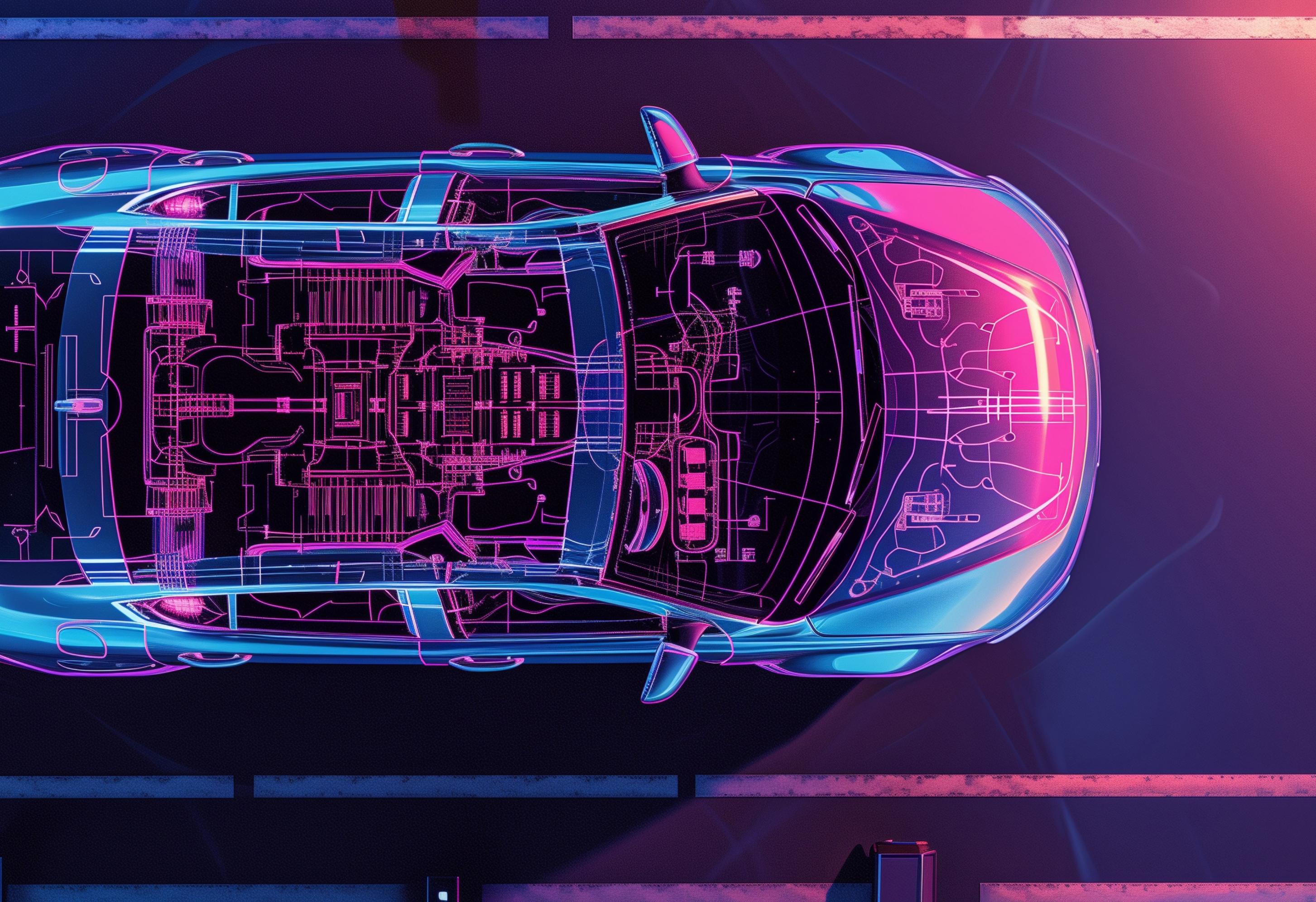
The automotive industry is transitioning to a single Ethernet-based backbone. This enables vehicles to be divided into "zones,"which interact with a centralized computing platform.
Optimizing power consumption is crucial for battery-powered devices. With ST MEMS sensors' Machine Learning Core (MLC), decision-tree classification runs directly inside the sensor. 30
In AI,"inference" is a model’s ability to make decisions from live data. Using a low-power computer with an inference accelerator near the data source enhances speed, autonomy, security, and privacy.
PROTECTIPONEXTERNALMEMORY
Many microcontrollers on the market provide storage density in the range of few Megabytes. External memory can be a better solution.


Data protection and lifespan management are critical in SSDs, particularly in embedded computing applications.
GaN will soon be able to address all application sectors from the low 10s of watts up to 100s of kilowatts.
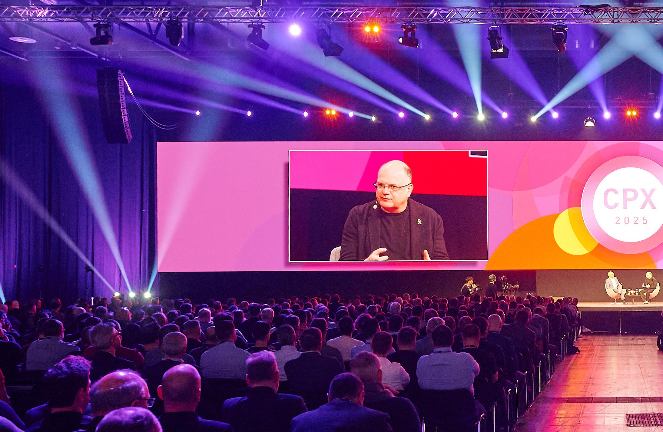
AI is both the biggest threat and the most powerful tool for cyber defenders. Eventually security solutions will become autonomous, self adapting systems, said Check Point Software in its annual CPX 2025 event in Vienna.
Cybersecurity is transitioning towards fully autonomous systems where artificial intelligence monitors, anticipates, and prevents attacks independently. Check Point's vision is to create self-healing security that not only responds to threats but prevents them before they even emerge, said the company’s Head of Research, Nataly Kremer, at the CPX2025 event in Vienna.
At the core of Check Point’s development plan is a hybrid mesh architecture that securely integrates cloud services with on-premises systems.
- Not all data should be moved to the cloud. That’s why we believe in an open platform that enables collaboration

- AI can already detect if a router has a vulnerability or if security policies are outdated. Some customers have rules that are over ten years old and haven’t been updated. AI not only monitors these rules but also updates them automatically to match emerging threats, Nataly Kremer said.
between different products, including solutions from other vendors, said Nataly Kremer, the Chief Product Officer and Head of R&D Check Point.
The advancement of cybersecurity is built on Check Point’s Infinity platform, which is based on three key principles: a unified product, centralized management, and seamless collaboration between different security solutions. Check Point’s gateways do not just block malicious traffic—they also share threat alerts with security products from other vendors, all happening automatically.
This is what we mean by a platform: the ability to connect and automate security management so that threats are countered collaboratively across different systems without manual intervention, Kremer clarified.
Artificial intelligence is becoming an increasingly crucial part of cybersecurity. Last year, Check Point introduced AI Copilot, a tool that helps analyze threats and accelerates response times. However, current AI is still reactive—the next step is proactive protection.
Check Point’s long-term goal is fully autonomous cybersecurity, where firewalls and other security systems
update themselves independently and in real time.
- A fully autonomous firewall is our ultimate goal, but it must be 100% reliable. Achieving this could take a year or two, depending on technological advancements. Said Kremer.
Autonomous cybersecurity is not just a technological leap—it represents a fundamental shift in the entire industry’s operating model. By moving towards predictive and self-healing security, organizations can achieve a new level of protection, where systems continuously adapt to evolving threats without human intervention.
Cybercriminals have begun leveraging new open-source Chinese AI models, such as DeepSeek and Alibaba's Qwen. According to Sergey Shykevich, head of Check Point’s Threat Intelligence group, cybercriminals were discussing DeepSeek even before its official release, and Alibaba’s recently introduced Qwen is already being used for malware development.
- Cybercriminals claim that Qwen is more accurate and superior to DeepSeek, with its biggest advantage being free availability," Shykevich explains. Open-

source LLM models available on platforms like GitHub, such as Qwen, do not differ significantly from GPT models, but their more flexible data usage during training and less restrictive user agreements make them attractive to criminals.
Although these new Chinese LLM models raise concerns, Shykevich emphasizes that their development is not part of a larger state-driven agenda but rather a result of commercial competition.
- Alibaba released Qwen during the Chinese New Year, and it appears to be aiming to compete directly with DeepSeek.
According to Shykevich, the risks associated with these models remain
unchanged, regardless of which AI model is used. Challenges related to privacy, GDPR compliance, and AI accountability persist. The question of whether LLM models store private data also remains open.
- It depends on how the AI is used. We don’t have a definitive answer yet.
So far, there have been no reports of advanced malware developed with Qwen being widely used, but experts believe it is only a matter of time.
- Cybercriminals are not traditionally coders but rather developers in a broader sense, Shykevich points out.
The new AI-driven methods are not limited to generating malicious code. AI is also being used for text translation and tool automation, speeding up and

- Simply checking a few security settings does not guarantee protection,
enhancing criminal operations.
While these new AI models are changing the ways cybercriminals operate, the fundamental nature of cyber warfare remains the same, according to Shykevich. - This has always been a cat-and-mouse game. Our goal is to stay ahead of the criminals, he concludes.
Viivi Tynjälä, Check Point´s Country Manager for Finland and the Baltics, reminded that many companies still hold the false belief that their systems are fully protected.
- Corporate networks are most frequently breached through email. Statistics show that over 70% of cyberattacks originate from email-based threats. Are Finnish companies’ emails well-protected? Tynjälä’s answer is blunt: “No.”
- Even though many companies assume their email security is sufficient, in reality, it often remains just an assumption. We offer businesses a ‘Health Check’ analysis, where we test their systems' security over a few weeks. More often than not, this report uncovers serious flaws, such as miscategorized emails. For instance, phishing emails may end up in the spam folder but are not effectively blocked. This checkup is often an eye-opening experience for companies.


Reijo Holopainen ETN
At the Verkosto 2025 trade fair, the digitalization of energy networks and infrastructure was clearly in focus. The most significant topic of discussion was the role of digital twins in remote control and automation of industrial systems. At the same time, the EU's F-gas regulation is forcing the energy sector to reform, and the use of 3D geospatial data is revolutionizing infrastructure construction.
A digital twin, which is a real-time virtual model of a physical system, is quickly becoming a standard in the energy sector. Schneider Electric and other industry leaders presented solutions in which digital twins enhance monitoring and maintenance efficiency. Predictive maintenance and remote fault diagnostics reduce downtimes, making electrical and information networks more reliable and efficient. The direct bidirectional data connection from the control center to the system allows realtime monitoring and optimization, improving operational efficiency. DT solutions are already in use in nuclear power plants, data centers, and power distribution substations, where they offer significant advantages in system
management and maintenance.
THE EU F-GAS REGULATION – THE BAN ON SF6 DRIVES INNOVATION
SF6 gas, widely used as an insulator in electrical equipment, is a highly harmful greenhouse gas. The EU's F-gas regulation, which came into effect in 2024, imposes phased restrictions on the use of SF6, forcing power distribution operators to rapidly adopt new solutions. The use of SF6 in medium voltage systems will end as early as 2026, putting pressure on the development of new insulation technologies. Electrical equipment manufacturers such as Schneider Electric have introduced alternatives where oxygen-based
mixtures provide a safe and environmentally friendly substitute for SF6. The change has broad implications for energy networks, infrastructure, and industrial electrification, requiring adaptation through new technologies.
3D GEOSPATIAL DATA ENHANCES INFRASTRUCTURE CONSTRUCTION
The documentation and accuracy of underground infrastructure construction are improving with new geospatial data solutions. Groundhawk Oy showcased its 3D modeling of fiber optic cable and earthwork projects, combining satellite positioning and artificial intelligence. Centimeter-accurate 3D modeling reduces errors and speeds up

documentation, ensuring precision in cable and pipe infrastructure. AI-based quality verification ensures that cable and protective location data are reliable, enabling more efficient project management. The Infrakit platform’s point cloud data allows real-time data sharing between construction sites and control centers, improving infrastructure processes and coordination among different stakeholders.
Direct current (DC) is becoming more common in electric vehicle charging
stations and power plant sites, but it presents significant safety risks. The uninterrupted arc of direct current can create life-threatening situations, highlighting the need for new protective solutions.
Schneider Electric’s arc protection solutions interrupt current within milliseconds, significantly improving workplace safety and reducing the risk of severe accidents. Alternating current (AC) protection technologies continue to evolve as well, with ABB presenting a new, highly effective arc protection solution that offers improved safety for electrical installations and networks.
The Verkosto 2025 trade fair highlighted that the digital twin is a key technology in the automation of energy networks and infrastructure construction. At the same time, EU regulations such as the Fgas regulation are forcing the industry to transition to new environmentally friendly solutions.
3D geospatial data and artificial intelligence are transforming industry practices, and challenges related to DC safety must be addressed quickly. Amid these changes companies are developing new innovations that are driving energy and data networks toward a smarter and more sustainable future.
Teams from HZB and Humboldt University Berlin have presented a CIGSperovskite tandem cell that sets a new world record with an efficiency of 24.6%, certified by the independent Fraunhofer Institute for Solar Energy Systems.
Thin-film solar cells require little energy and material to produce and therefore have a very small environmental footprint. In addition to the well-known and market-leading silicon solar cells, there are also thin-film solar cells, e.g. based on copper, indium, gallium and selenium, known as CIGS cells. CIGS thin films can even be applied to flexible substrates.
Now, experts from HZB and Humboldt University Berlin, have developed a new tandem solar cell that combines a bottom
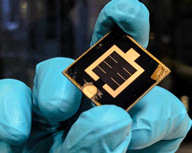
cell made of CIGS with a top cell based on perovskite. By improving the contact layers between the top and bottom cells, they were able to increase the efficiency to 24.6 %. This is the current world record, as certified by the Fraunhofer Institute for Solar Energy Systems ISE in Freiburg, Germany.
As always, this record cell was the result of a successful team effort: the top cell was fabricated by TU Berlin master's student Thede Mehlhop under the supervision of Stefan Gall. The perovskite absorber layer was produced in the joint laboratory of HZB and Humboldt University of Berlin. The CIGS sub-cell and contact layers were fabricated by HZB researcher Guillermo Farias Basulto. He also used the high-performance cluster system KOALA, which enables the deposition of perovskites and contact layers in vacuum at HZB.
Prof.essor Rutger Schlatmann, spokesman for the Solar Energy Department at HZB is confident that CIGS-perovskite tandem cells can achieve much higher efficiencies, probably more than 30%.
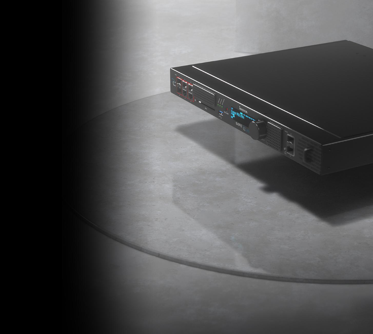
Technology company Insta has introduced a new highsecurity encryption product, the Insta SafeLink Secret encryption device, specifically designed to secure Security Class II (SECRET) data transmission. This makes Insta the first Finnish company to bring such a high-security encryption solution to the market.
The Insta SafeLink Secret encryption device has been developed to meet the needs of national security authorities, the Defense Forces, and other organizations handling critical information. Significant investment has been made in its development, and its compliance assessment process is expected to be completed by June 2025.
- The functionality related to performance improvement has also been patented. The encryption device uses quantumsafe algorithms, meaning it will withstand decryption attempts made by future quantum computers, says Mika Joutsenvirta, Director of Insta’s Cybersecurity Business.
A key feature of the Insta SafeLink Secret encryption device is its completely redesigned hardware architecture. One significant technical innovation is the so-called red-black separation, where plaintext signals are encrypted directly at the hardware level rather than in software. This ensures that potential software vulnerabilities cannot lead to data leaks into untrusted networks.
- The encryption devices are manufactured and assembled in Finland, and all possible components that can be produced domestically are also made in Finland. The design, product development, production, maintenance, and customer support are all entirely domestic," Joutsenvirta states.
Finland’s NATO membership has increased the demand for
high-security encryption devices. Insta is now seeking NATO SECRET approval for the SafeLink Secret solution, which will open doors to international markets.
- NATO membership was also the reason we sought NATO-R approval for our existing SafeLink product, making it the first of its kind in Finland. We see a growing need for highsecurity encryption devices both nationally and internationally, Joutsenvirta says.
Finland's Cybersecurity Strategy and the recent Defense Report have emphasized the importance of self-sufficiency in critical encryption technology. The Insta SafeLink Secret encryption device is a response to this need, enabling Security Class II data transmission with a fully domestic solution.
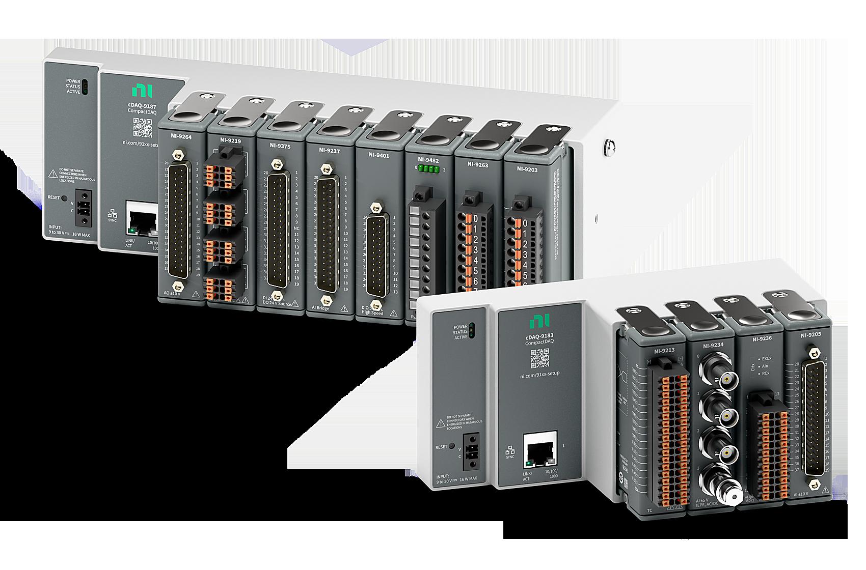
Emerson, the current owner of the former NI brand, has introduced new NI CompactDAQ series devices that provide a more affordable and flexible solution for data acquisition over Ethernet. The cDAQ-9187 and cDAQ-9183 devices, along with the NI-9204 input module, enable cost-effective testing without compromising performance.
These are the first entry-level Ethernet solutions in the NI CompactDAQ series. They are designed for conducting electrical and sensor measurements remotely and are particularly suited for systems requiring long-distance, reliable data acquisition.
The new cDAQ-9187 and cDAQ-9183 modules feature a single Ethernet port and maintain NI’s traditionally high-quality synchronization but without external trigger lines, reducing costs. Additionally,
these devices include QR codes that provide users with direct access to installation instructions and documentation.
The new NI-9204 ±10V input module, in turn, offers a more cost-effective alternative to previous popular modules. It enables 16-bit A/D conversion in either differential or single-ended configurations, allowing for precise and reliable measurements.
Emerson’s software development updates bring more customization options to NI FlexLogger users. The company has launched a new GitHub repository where users can download, share, and develop FlexLogger add-ons. The collection includes ready-made templates as well as add-ons enabling more efficient automation and customization of testing processes.
Microchip Technology has leveraged artificial intelligence to assist software developers and embedded systems engineers in writing and debugging code. The company has released the new MPLAB AI Coding Assistant, a free extension for Microsoft Visual Studio Code.
The tool is based on the popular opensource Continue assistant and includes Microchip’s proprietary AI-powered chatbot for real-time support. The chatbot enables an interactive chat feature, allowing developers to analyze and modify code directly from the sidebar. This support enhances the programming experience by providing tailored, up-todate advice and insights, particularly

related to Microchip’s products.
The chatbot is continuously updated, and its additional features include advanced auto-completion, editing tools, and error detection, which help developers efficiently refine their code. Moreover, developers can use integrated search
Infineon has announced that its PSOC 4 microcontroller family now features Multi-Sense capabilities. Infineon expands its leading capacitive sensing technology CAPSENSE with a new, proprietary inductive sensing technology, as well as a non-invasive and non-contact liquid sensing solution. PSOC 4000T is the first device to feature the company’s fifthgeneration CAPSENSE and MultiSense. The supported sensing technologies can be combined in a single PSOC 4 MCU to optimize performance, enable new use cases (e.g., underwater inductive sensing buttons) or realize cost savings.-> etn.fi/17223
STMicroelectronics is the first company to put quad-band, multi-constellation design, needed for precise GNSS positioning accurate to a few centimeters, on a single die. The new Teseo VI chips and modules will be core building blocks of advanced driving systems (ADAS), smart in-vehicle systems, and safety-critical applications such as autonomous driving. They have also been designed to improve positioning capabilities in multiple industrial applications.
-> etn.fi/17222
functionalities to access Microchip’s documentation directly within the development environment.
Unlike many other coding assistants on the market, the MPLAB AI Coding Assistant’s sidebar chat can generate block diagrams directly in the VS Code interface instead of providing only textbased responses. This feature, combined with easy access to Microchip’s continuously updated documentation library for microcontrollers and microprocessors, speeds up development and improves code accuracy.
The MPLAB AI Coding Assistant is available for free, but some advanced features require a paid license.
The development of smart homes and IoT devices took a leap forward when Silicon Labs unveiled its new MG26 system-on-chip (SoC). It is the market's first Matter-compatible chip integrating advanced artificial intelligence and machine learning acceleration. This innovation enables the development of smarter and more energy-efficient IoT devices without relying on cloud services.
Matter has established itself as the universal standard for smart homes, allowing seamless interoperability between devices from different manufacturers. With the MG26 chip, Matter devices can now leverage machine learning directly through edge computing. This means that smart home devices can make real-time decisions faster and more efficiently without a constant internet connection.
MG26's machine learning acceleration enables predictive maintenance, where IoT devices detect wear and potential failures in advance by analyzing sensorgenerated data. The chip also identifies anomalies and intrusions, enhancing
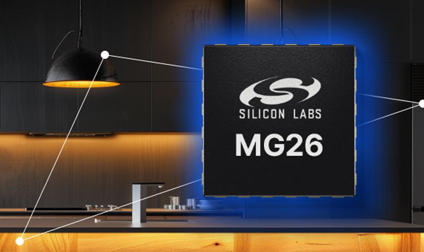
smart home security by detecting unusual sounds or movements.
With MG26, voice and gesture control can also be integrated into smart home devices: lights and other home appliances can respond to user commands without requiring cloud-based processing. The performance is also
sufficient for image recognition, which can be utilized in smart cameras and automated lighting systems.
The first MG26-based products are expected to hit the market in 2025, potentially revolutionizing how homes and buildings incorporate AI into everyday life.
VTT Technical Research Centre of Finland and IQM Quantum Computers, one of the global leaders in superconducting quantum computers, have completed and launched Europe’s first 50-qubit superconducting quantum computer, now open to researchers and companies through the VTT QX quantum computing service.
The new 50-qubit quantum computer further strengthens Finland’s position among the countries capable of developing and investing in quantum computing. Finland first announced its efforts in quantum computing development back in November 2020 with a total budget of EUR 20.7 million from the Finnish government to develop a 50-qubit quantum computer.
The 50-qubit quantum computer opens today for use by companies and researchers in universities and research institutes through the VTT QC quantum computing service. The quantum computer offers industries an opportunity to develop applications for quantum computing and to work on them in a practical way.
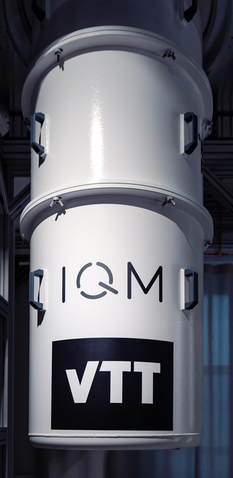
Quantum computers were developed as a joint development project, where both parties, VTT and IQM, developed part of the technology. VTT especially developed the superconducting TWPA amplifiers, used for readout of the qubit signals, as well as quantum processor chip-level integration and packaging solutions. The superconducting TWPA amplifiers developed and manufactured by VTT are currently the world’s leading components, and they are in high demand within the quantum technology industry in Europe.
VTT’s spin-off company, Arctic Instruments, is commercializing VTT’s TWPA technology.
VTT also made significant leaps forward in the manufacturing of qubits and integration technologies, and VTT is now offering them as a commercial service. The manufacturing methods used in quantum technologies now include the Josephson junction technology, superconducting Through Silicon Vias (TSVs) and superconducting flip chip integration methods. VTT has also launched another quantum technology spin-off, SemiQon, which is developing semiconducting qubits.

The European Union's new NIS2 directive tightens cybersecurity requirements across multiple sectors but leaves the protection of higher education and research at a worryingly light level. According to Juha Malmivaara (pictured above), the CISO of the Tampere higher education community, this poses a serious security risk, as universities are already targets of international intelligence and cyberattacks.
At the Prevent pre-seminar of the Disobey hacker event, Malmivaara pointed out that while universities are not officially classified as critical for national security, they handle vast amounts of sensitive information that interests international actors. According to him, Russia, China, Iran, and North Korea, in particular, are actively interested in Finnish research institutions.
This is not surprising—Finnish universities develop technologies that may also have military applications. Examples include 6G networks, drone technology, and signal communication. Additionally, the EU's Chips Act, which aims to reduce dependence on Chinese and Taiwanese semiconductor manufacturing, makes Finnish research institutions an even more attractive target for foreign actors.
Universities operate in the spirit of international cooperation, which makes infiltration easy. There are multiple ways to gain access to university networks: a postgraduate student's credentials grant access to extensive data networks, an official university login can be obtained for just 40 euros through an open university course, and the HAKA authentication system that every student udses, allows access to almost all university networks.
- Universities are a springboard for intelligence operations – they provide access to data repositories, networks, and decision-makers, Malmivaara stated. This makes them a strategically important target, yet they are not protected in the same way as other critical infrastructures.
Malmivaara provided concrete examples of foreign actors attempting to influence Finnish research or infiltrate universities. One case involved a Russian spy who infiltrated Norway to study hybrid threats. In another case, Iranian nationals participated in research whose results could be used for military development.
Although universities can implement technical security measures—such as blocking logins from Russia and Iran—in practice, research networks are so vast that cybersecurity is difficult to manage effectively.
The war in Ukraine has demonstrated that technological expertise is crucial in times of crisis. Finnish universities have been involved in developing drone warfare technology, and similar projects may become even more significant in the future. However, without stricter security measures and risk management, universities may serve as gateways for foreign intelligence and the misuse of technology.
According to Malmivaara, universities should work more closely with authorities and improve background checks on personnel.- Our main task is to protect researchers from themselves, he said.
As it stands, the NIS2 directive does not require universities to implement strict cybersecurity practices, even though they develop critical technology.
Silicon Labs has announced that its MG26 family of wireless SoCs is now generally available through Silicon Labs and its distribution partners. As the industry's most advanced, highperformance Matter and concurrent multiprotocol solution to date, the MG26 SoC features double the Flash and RAM of other Silicon Labs multiprotocol devices, advanced AI/ML processing, and best-inclass security to empower developers to design futureproof Matter applications. Silicon Labs is the only Matter SoC device maker that allows customers to customize their order with their own Matter device attestation certificates (DAC).-> etn.fi/17206
KONTRON PI-TRON UPDATED
Kontron used Embedded World 2025 in Nuremberg to launch the new BL Pi-Tron CM5 module. The new industrial board is designed to meet the demand for off-the-shelf products and an open software environment in the embedded industry. It is based on the latest Compute Module 5 from Raspberry Pi Ltd. The BL Pi-Tron CM5 offers significantly increased performance over its predecessor. The Broadcom BCM2712, a Quad Core Cortex®A76, 64-bit SoC running at 2.4 GHz provides high processing power. -> etn.fi/17198
Researchers at Ohio State University have developed a battery that can convert nuclear energy into electricity. Using a combination of scintillator crystals, high-density materials that emit light when they absorb radiation, and solar cells, the team demonstrated that ambient gamma radiation could be harvested to produce a strong enough electric output to power microelectronics. Tests showed that when cesium-137 was used, the battery generated 288 nanowatts. With cobalt-60 the battery produced 1.5 microwatts, which is enough to switch on a tiny sensor. -> etn.fi/17214
The automotive industry is revolutionizing the driving experience with innovative smart cockpits, where large displays and new technologies such as OLED and microLED panels seamlessly combine functionality and design. However, these advancements bring challenges for integrating capacitive touch technology, as thinner structures and an increasing number of touch electrodes can impact sensitivity and accuracy.
Microchip has addressed this challenge by introducing the ATMXT3072M1 and ATMXT2496M1 touchscreen controller families. These single-chip solutions offer up to 112 reconfigurable touch channels—or 162 equivalent channels in ultra-wide mode—enabling the implementation of large, curved, and free-form touch displays up to 20 inches in size
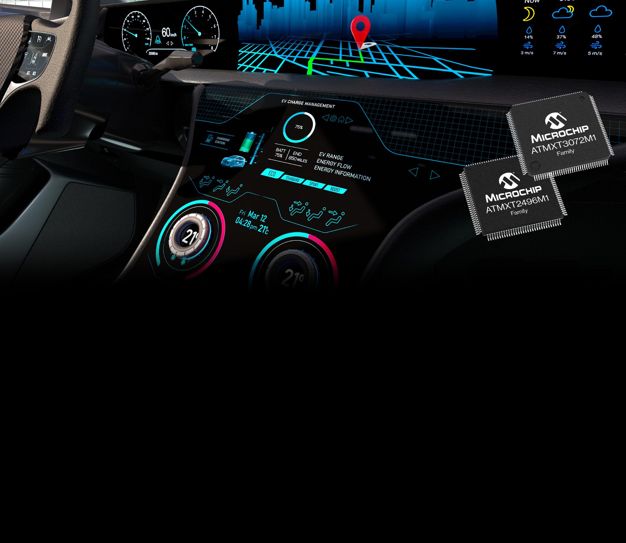
(16:9 format) and 34 inches in size (7:1 format).
The new controllers are part of the maXTouch product family and utilize Microchip’s patented Smart Mutual touch acquisition method and algorithms that improve the touch signal-to-noise ratio (SNR) by up to +15 dB compared to the previous generation. This enables fast and reliable touch detection even in demanding display environments.
The controllers support ASIL-A and B safety standards and have been developed in accordance with the ISO 26262 functional safety management system. They also include cybersecurity features such as the SHA-512 cryptographic hash function, enabling secure over-the-air (OTA) updates in compliance with the ISO 21434:2021 standard.
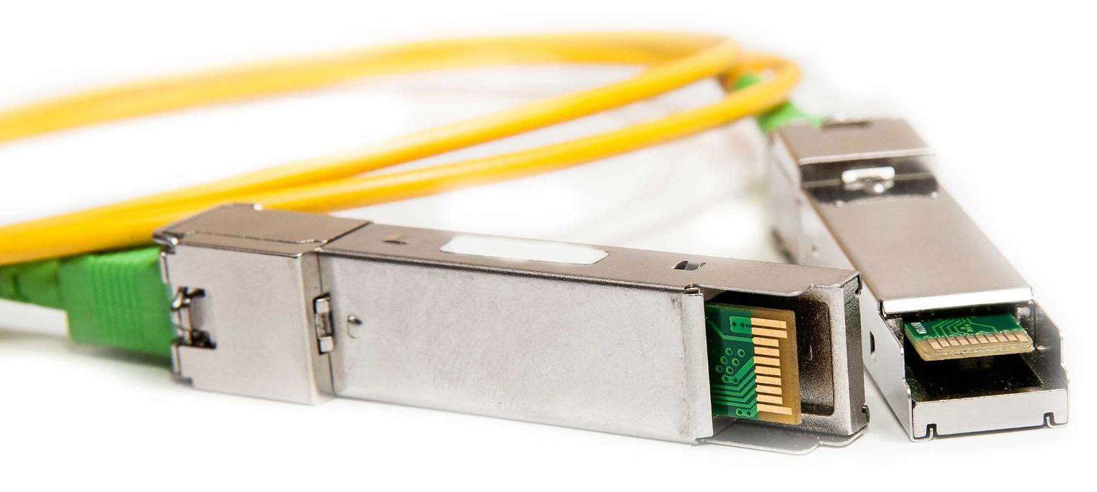
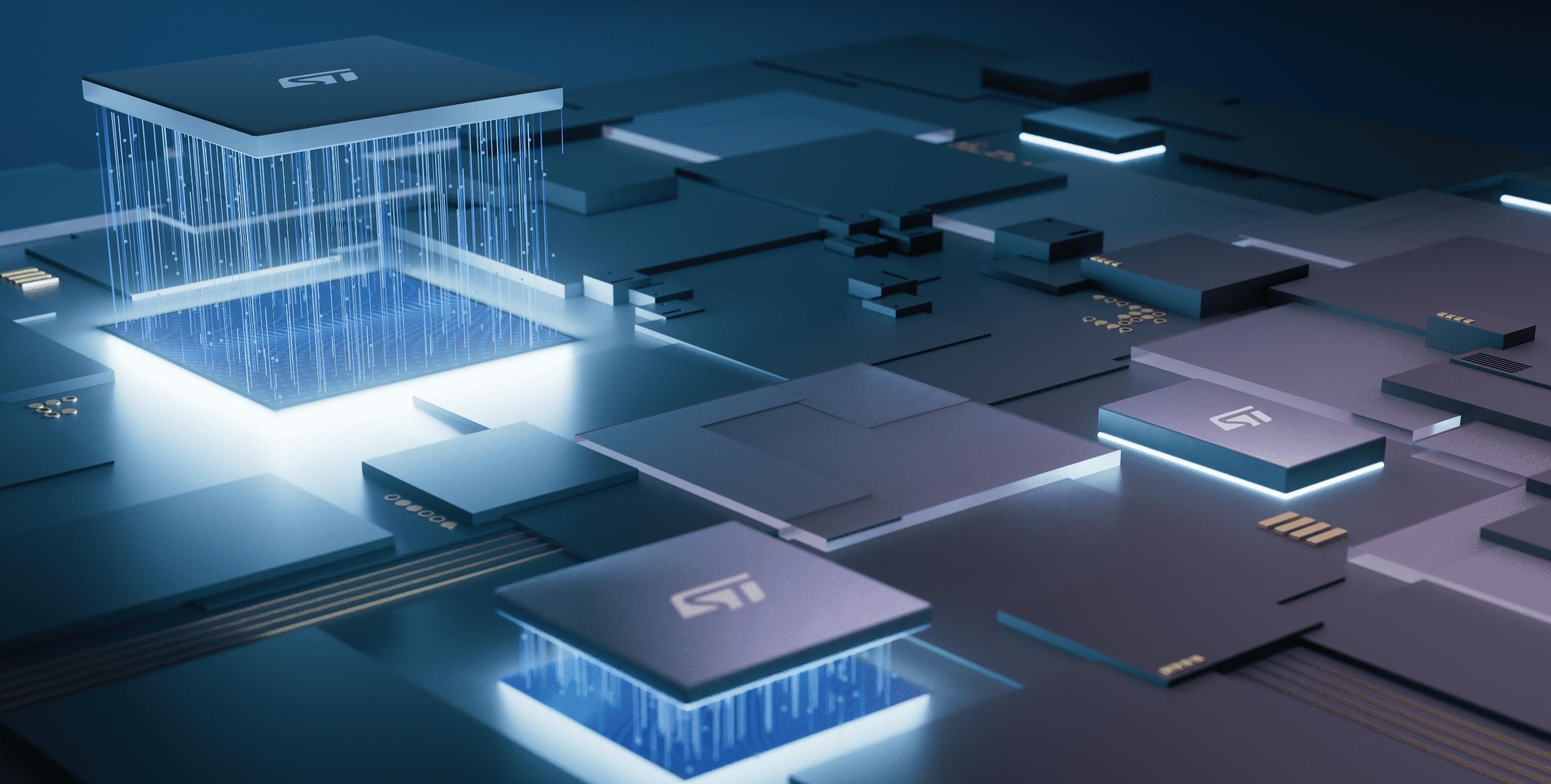
STMicroelectronics has unveiling its next generation of proprietary technologies for higher-performing optical interconnect in datacenters and AI clusters. With the exponential growth of AI computing needs, challenges arise in performance and energy efficiency across computing, memory, power supply, and the interconnections linking them.
ST is helping hyperscalers, and the leading optical module provider, overcome those challenges with new silicon photonics and next-gen BiCMOS technologies, scheduled to ramp up from the second half of 2025 for 800Gb/s and 1.6Tb/s optical modules.
At the heart of interconnections in a
datacenter are thousands, or even hundreds of thousands, of optical transceivers. These devices convert optical into electrical signals and vice versa to allow data flow between graphics processing unit (GPU) computing resources, switches and storage. Inside these transceivers,
ST’s new, proprietary silicon photonics (SiPho) technology will bring customers the ability to integrate multiple complex components into one single chip, while ST’s next-gen, proprietary BiCMOS technology brings ultra high-speed and low power optical connectivity, which are key to sustain the AI growth.
ST’s SiPho technology combined with the ST BiCMOS technology are a unique 300mm silicon platform to serve the optical market. Both technologies are being industrialized and will be manufactured in ST’s Crolles (France/ Europe) 300mm fab.
Amazon Web Services (AWS) has announced its first-ever quantum computing chip. Developed at the AWS Center for Quantum Computing at the California Institute of Technology (Caltech), the Ocelot chip marks a significant step toward scalable and faulttolerant quantum computers. Ocelot is specifically designed to enhance quantum error correction, reducing the cost of quantum computation by up to 90% compared to traditional methods.
Ocelot is based on cat qubit technology, which naturally suppresses certain types of errors, simplifying error correction. AWS has successfully integrated this technology into a semiconductor chip that can be manufactured using existing electronics industry processes. This advancement makes quantum computers more practical and scalable than before.
The Ocelot chip consists of two integrated semiconductor chips, each approximately 1 cm² in size, connected electrically. The chip includes a total of 14 core components: 5 cat qubit units that perform quantum computations, 5 buffering circuits that stabilize data qubits, and 4 additional qubits for error detection.
Cat qubit technology relies on oscillators that generate precisely timed electrical signals. AWS material scientists have developed a specialized manufacturing process that enhances oscillator performance by using tantalum as a superconducting material.
One of the biggest challenges in quantum computing is its sensitivity to external disturbances, such as temperature fluctuations and cosmic rays. Quantum error correction addresses this problem by encoding quantum information across multiple physical qubits, allowing errors to be detected and corrected. Traditionally, quantum error correction requires vast resources, but Ocelot’s innovative architecture reduces this need by a factor of 5 to 10.
Although Ocelot is still a prototype, its promising results pave the way for largescale quantum computers. AWS continues its development efforts and maintains close collaboration with academic researchers. With this new technology, quantum computing could transition from research labs to commercial and industrial applications in the coming years.
STMicroelectronics has announced the new DCP3601 buck converter, which combines a compact size, high efficiency, and a simple design. Requiring only six external components, the DCP3601 enables cost-effective and compact circuit designs.
ST’s new converter operates with an input voltage range of 3.3V to 36V and can deliver an output current of 1A, making it an ideal choice for applications such as smart meters, home appliances, and industrial 24V conversions. Its synchronous rectification and 1 MHz switching frequency ensure high efficiency in all operating conditions, reaching up to 91% efficiency at a 600 mA load (12V input, 5V output).
The DCP3601 also offers a mode selection feature, allowing either forced PWM (for noise-sensitive applications) or pulse skipping at light loads to minimize power consumption. Additionally, alternative models provide frequency modulation to reduce noise at a 1 MHz switching frequency.
Researchers at the University of Gothenburg have made a significant breakthrough in computing technology. They have developed a new type of computer that could offer an energy-efficient alternative to quantum computers and operates at room temperature. The research utilizes spintronics, a technology that processes information highly efficiently using magnetism. The scientists have successfully controlled and synchronized spin waves, enabling a new approach to computational tasks. This could lead to the next generation of Ising machines, which solve complex optimization problems much faster and more energyefficiently than current computers.-> etn.fi/17197
ZeroPoint Technologies AB of Sweden has announced a breakthrough hardwareaccelerated memory optimization product that enables the nearly instantaneous compression and decompression of deployed foundational models, including the leading large language models (LLMs). The new product, AI-MX, will be delivered to initial customers and partners in the second half of 2025 and will enable enterprise and hyperscale datacenters to realize a 1.5 times increase in addressable memory. -> etn.fi/17193
13 Ghz SEEMS TO WORK FOR 6G
German Rohde & Schwarz and Qualcomm Technologies have successfully validated the highthroughput performance of a 5G NR connection at 13 GHz, a band that falls within the proposed FR3 frequency range. This milestone paves the way for the next generation of wireless networks. The companies successfully validated the performance of Qualcomm´s 5G mobile test platform (MTP) using the CMX500 5G one-box signaling tester in a maximum throughput use case at 13 Ghz. -> etn.fi/17191
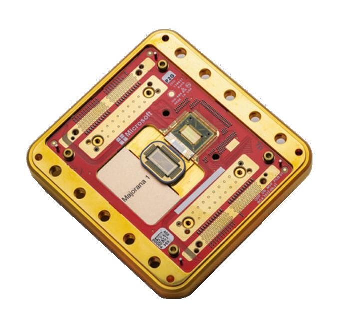
Microsoft has announced a significant breakthrough in quantum computing development. The company’s new "Majorana 1" quantum processor is based on topological qubits, which could revolutionize the field by providing a decisive advantage in managing quantum errors. If Microsoft’s approach proves successful, it could surpass competitors and enable a faster transition to large-scale quantum computing adoption.
The biggest challenge in quantum computing has been quantum error management. Traditional quantum systems, such as superconducting qubits and ion traps, are highly sensitive to external disturbances and require complex error correction methods. As a result, today’s quantum computers need hundreds of physical qubits to produce just a single reliable "logical qubit."
Microsoft believes it has solved this problem by developing a new type of quantum processor based on topological qubits. At the core of this technology are Majorana particles, theoretical quasi-particles capable of storing quantum information far more stably than traditional methods.
Majorana particles, first predicted in 1937 by Italian physicist Ettore Majorana, are unique in that they act as both particles and antiparticles simultaneously. They do not naturally occur in nature, but Microsoft has successfully created them in the laboratory using a new material called a topoconductor. This combination of superconducting aluminum and semiconductor indium arsenide enables topological superconductivity,
allowing Majorana particles to form and be manipulated.
The idea behind topological qubits is that Majorana particles can be braided, meaning their positions can be swapped in a specific manner. This changes the quantum state without exposing the quantum information to external interference. As a result, topological qubits are naturally error-resistant, significantly reducing the computational overhead required for quantum error correction.
Another major innovation in Microsoft’s technology is its approach to handling quantum information. Traditionally, quantum programming relies on delicate, analog operations, where qubit states are altered using precisely controlled pulses. In contrast, Microsoft’s system performs computations through measurements, allowing quantum error correction to be implemented with simple digital commands. This could make large-scale quantum computing much more practical.
Microsoft has long lagged behind competitors such as Google and IBM in quantum computing development. Google's 2019 demonstration of "quantum supremacy" and IBM’s advancing quantum processors have kept them at the forefront of the industry. However, Microsoft has chosen a more ambitious but riskier approach, which could prove victorious in the long run.
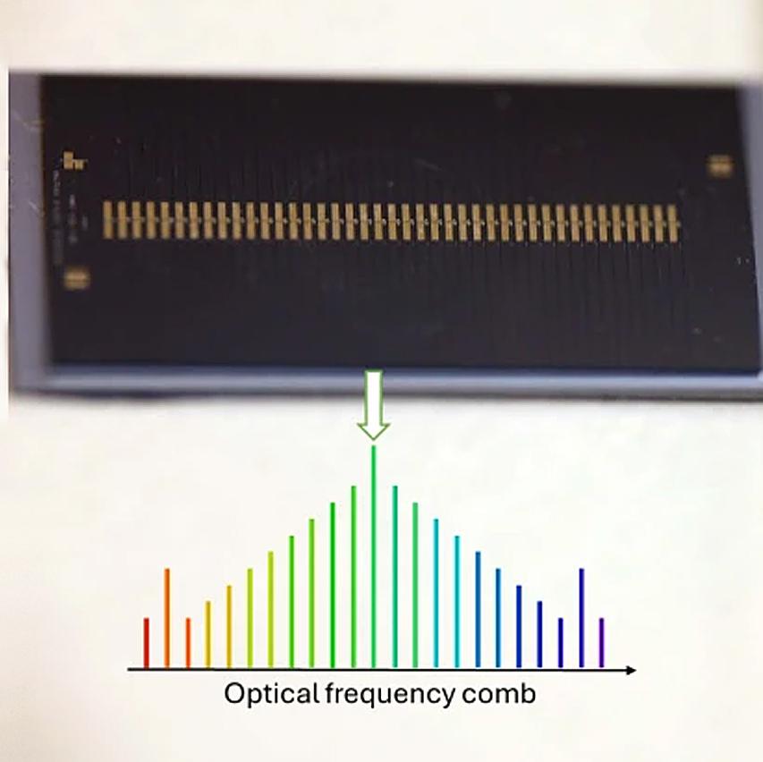
The accuracy of current GPS systems is only a few meters, but new technology could bring positioning accuracy down to the centimeter level. Researchers from Purdue University and Chalmers University of Technology have developed a chip-based frequency comb technology that could revolutionize navigation, autonomous vehicles, and precision measurement systems.
Accurately determining time and location relies on atomic clocks used by GPS satellites. Current atomic clocks are based on microwave frequencies, but much more accurate optical atomic clocks use light frequencies. The problem has been that these devices are large and complex, limiting their practical use.
The research team has developed a frequency comb (optical frequency comb), a small chip-based device that enables
the miniaturization of optical atomic clocks. This advancement could make ultra-precise timekeeping accessible even for mobile phones and vehicles.
- In the future, we may see GPS systems
capable of centimeter-level accuracy. This will particularly benefit autonomous vehicles and applications that require precise measurements, says Professor Minghao Qi from Purdue University.
A frequency comb consists of evenly spaced light frequencies, comparable to the teeth of a comb. It acts as a bridge between the high-frequency optical signals of an atomic clock and conventional electronic measurement systems.
The researchers solved a significant challenge by developing a chip-based system that can convert optical frequency into radio frequency without the need for large optical components. This enables significant downsizing of atomic clocks, making them feasible for use in satellites, remote sensing, and even portable devices.

Quality assurance in embedded software development gains new reinforcement as Nohau Solutions and Percepio AB of Sweden announce a new distribution partnership. Through this collaboration, embedded software developers will gain even better tools for code analysis, testing, and diagnostics.
One of the key solutions in this partnership is Percepio’s Tracealyzer, an advanced tool for real-time software performance analysis. It helps developers identify issues and optimization opportunities at an early stage. Combined with other Percepio tools, such as Detect, this provides a comprehensive approach to improving software quality and security.
Nohau Solutions’ CEO Andreas Dyrhed emphasizes that Percepio’s products complement their existing toolkit and open new possibilities across different stages of software development. Andreas Lifvendahl, CEO of Percepio, also sees great potential in the collaboration.
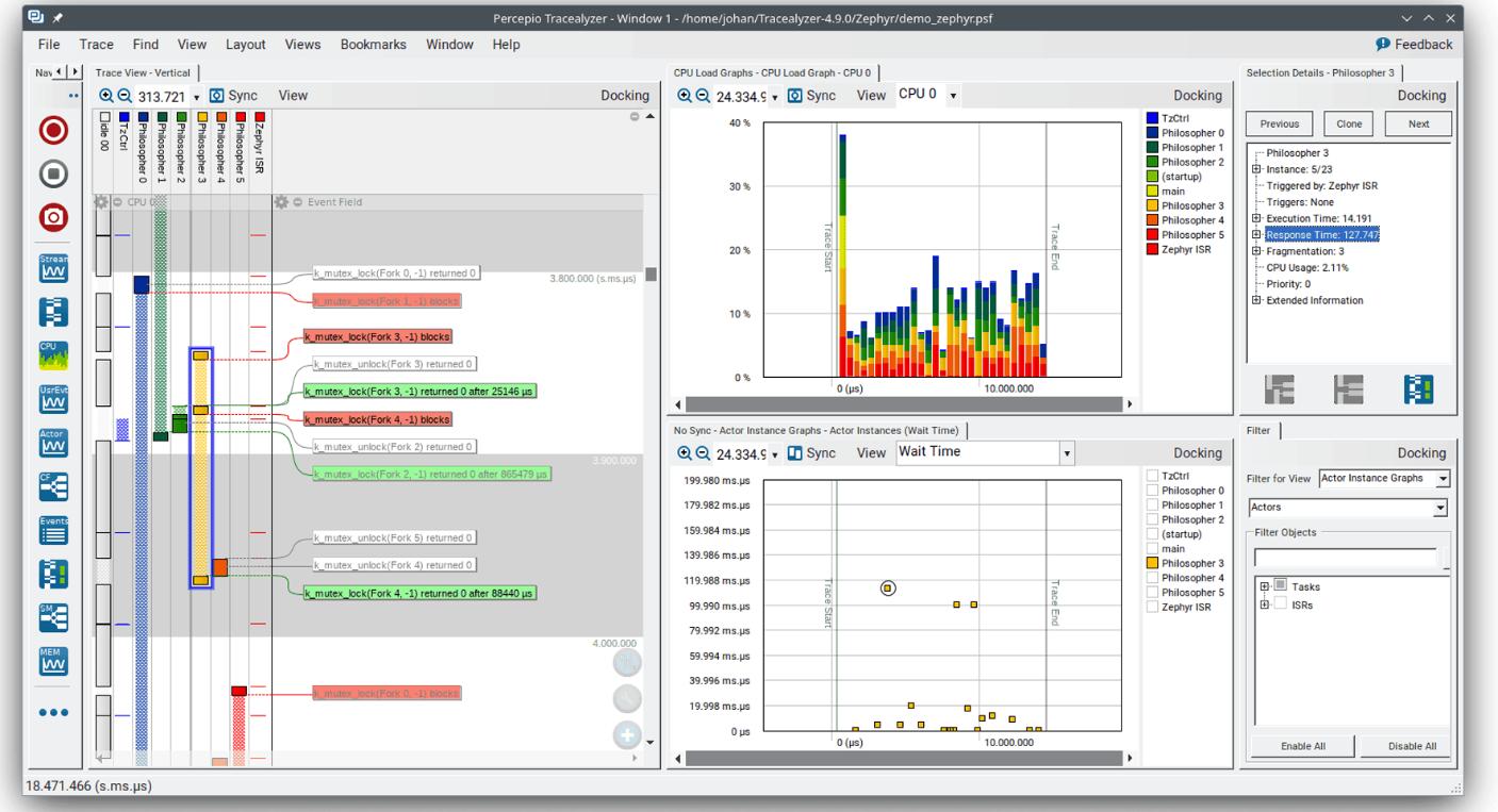
- We are committed to improving the quality and efficiency of embedded software. Continuous Observability is key to this, and we need partners who share this vision. Nohau Solutions is an excellent addition to our partner network, Lifvendahl says.
Researchers from Linköping University have developed a new method that allows all components of a perovskite solar cell to be recycled without using environmentally harmful solvents. The method enables the disassembly of the solar cell and the reuse of materials without compromising its performance.
The demand for energy is growing rapidly due to digitalization, advancements in artificial intelligence, and the electrification of transportation. The use of renewable energy is crucial in combating climate change, and solar energy is one of the most promising solutions. Traditional silicon-based solar cells have been on the market for over 30 years, but recycling them has proven to be challenging. The increasing disposal of old solar panels in landfills is becoming a growing problem.
- Currently, there is no efficient way to recycle silicon-based solar panels, which leads to large amounts of electronic waste, says Xun Xiao, a postdoctoral researcher at Linköping University.
Perovskite-based solar cells represent a new generation of solar energy solutions. They are cost-effective, lightweight, and
Thanks to this partnership, developers will have enhanced tools for software quality assurance, diagnostics, and optimization—accelerating the development process and improving the reliability of the final product.

flexible, allowing them to be installed on various surfaces, even on windows. Perovskite solar cells can convert around 25 percent of sunlight into electricity, which is comparable to the efficiency of traditional silicon panels.
Although perovskite solar cells have great potential, their shorter lifespan compared to silicon panels poses a challenge. Therefore, their recyclability is crucial. The production of perovskite materials involves small amounts of lead, which necessitates a responsible recycling process.
Traditionally, the recycling of perovskite solar cells has relied on dimethylformamide, a toxic and potentially carcinogenic substance. The researchers at Linköping University have developed a new method in which water serves as the solvent for dissolving and reusing perovskite. This approach allows for the direct recovery and reuse of highquality perovskite without degrading its performance.
The researchers now aim to scale up the method for industrial application to enable broader adoption.

In Finland the electronics sector had a turnover of 21 Billion EUR in 2023 and it employs 43 100 people. Computer and IT industry had a turnover of 20 Billion EUR and it employs 85 200 people.
In total these high tech industries cover for more than 50 per cent of Finnish exports. The technology sector does more than 65 per cent of all r&d investments in Finland.
ETN is a Finnish technology media for everyone working, studying or just interested in technology. Through website with daily news and technical articles, daily newsletters and columns ETN covers every aspect of high technology. Join us in 2025. See the media kit here.
Europe’s electronic component distribution market has been in a downturn, but now signs point to a steady recovery in 2025, says Mike Slater, the VP of Global Business Development at DigiKey.
What are the primary reasons the European electronic component distribution market is facing greater challenges compared to other regions?
- The European market is not necessarily facing greater challenges; it is just at a different point in the cycle right now. Over the long term, it’s a matter of timing more than anything.
The region has been in a down part of the cycle for a solid time. However, when I look at things globally, I see reasons to be optimistic. The European industry has a wide customer base that is very diversified in how their verticals line up. Like many other regions, Europe is poised to be successful in the long term from an electronics standpoint. Unfortunately, they’re just at the bottom of the cycle right now.
This year, we expect that with these natural industry cycles, we will see a tightening and business will start to improve throughout the year. We see 2025 as a strong year for consumption and encourage our customers to design with flexibility in mind. DigiKey is ready to move forward on this next extended cycle, which we think will be more of a gradual, sustained, steady upside instead of the crazy peak that we saw in 2021 and 2022.
Many key vertical markets in Europe will continue to develop further and drive growth, including renewable energy, automotive/electric vehicles, cellular networks, IOT, industrial automation and AI.
What role does the reliance on imported components play in Europe's struggle to stabilize its distribution market, and how are regional suppliers addressing this issue?
- Both Europe and the Americas rely on imported components to a high degree. It is a delicate balance to weigh the desire and need, in some cases, for regional diversity with cost analysis. Most customers don’t
want to pay more for their components to be built in-region, but it’s important to balance the competitiveness of both the component and end product with what you need to do for diversity and risk avoidance.
How is DigiKey dealing with the long lead times and increased costs of key electronic components, and how does this compare with global competitors?
- We deal with long lead times the way we have for the last 50 years, by continuing to make long-term investments in technology and internal advancements in our infrastructure, warehouse, systems and inventory to support our growing customer base. We have also added new financial technology to remain cost competitive. DigiKey continues to engage with our customers and suppliers and make investments to drive efficiencies.
While some companies pull back in making investments in technology and products in down markets, we are all in and continue to invest and make ourselves even better for our customers, taking this opportunity to position ourselves well for the future because the long-term nature of the electronic components business is going to be very strong. In 2024, we expanded our supplier partners by 455 new suppliers and added more than 1.1 million innovative products. We’re excited to continue offering engineers and designers even more industry-leading products in 2025. Areas such as automotive, AI, energy, industrial automation and IoT will be key growth drivers.
What impact does the limited availability of manufacturing hubs and fabs in Europe have on the region's ability to compete in the global electronic component market?
- The electronics business relies on Asia from a manufacturing standpoint. This doesn’t put Europe at a significant disadvantage in competing globally or vs the Americas, but it does make it a bit trickier to compete within Asia.

Suppliers are looking at having a varied approach to supporting things in the region. They want to have the right balance of risk tolerance in their manufacturing while finding areas that can support lowcost manufacturing.
What is DigiKey's predictions for European dist market in 2025? When will we return to real growth?
It depends what you call real growth! If real growth is a positive number, I believe we’ll see some positive numbers this year. We believe the European distribution market will grow this year, but we don’t anticipate double-digit growth.
The European region is vital to DigiKey, as it’s an area that always drives innovation and demand. DigiKey saw impressive customer count growth last year, finishing 2024 with the highest number of yearly customers ever. DigiKey’s customer counts grew in all regions in 2024, and Europe had the highest percentage of customer count growth overall. Some countries with positive revenue growth included the UK, Spain, Norway, Poland, the Netherlands, France and Italy. We saw excellent design and customer growth activity, setting the stage for the future from a market standpoint.
Henry Muyshondt Microchip Technology

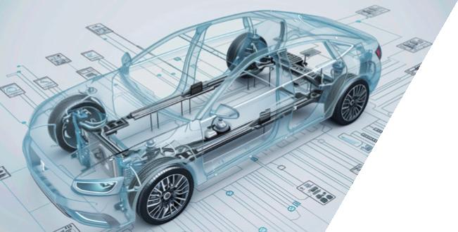
The automotive industry is transitioning to a single Ethernet-based backbone. This shift enables vehicles to be divided into "zones," each of which can interact efficiently with a centralized computing platform via an IP-based, ubiquitous Ethernet network.
The complexity and innovation of modern automobiles reflect broader advancements in technology. Today’s vehicles function as highperformance computing platforms, processing vast amounts of data and acting as datacenters on wheels. These vehicles integrate multiple subsystems that rely on seamless information exchange to enable automation, interacting with the physical world through an array of sensors and actuators.
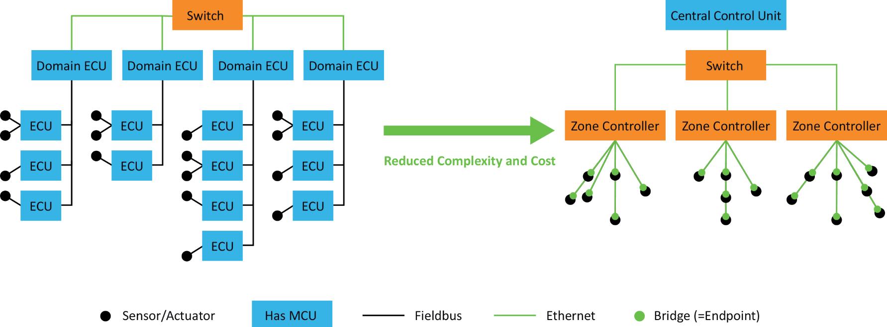
Traditionally, these subsystems employed communication technologies optimized for specific functions, resulting in domain-specific hardware architectures. Each domain required its own application-specific communication bus to transfer data, necessitating the use of gateway computers to
translate information between different systems. With as many as 20 networking standards in use, this approach led to significant complexity. Automakers sought a more streamlined solution—one that would unify communication infrastructure across the vehicle.
In response to this challenge, the automotive industry is transitioning to a single Ethernet-based backbone. This shift enables vehicles to be divided into "zones," each of which can interact efficiently with a centralized computing platform via an IPbased, ubiquitous Ethernet network. By collaborating with the IEEE, automakers helped define a physical layer standard requiring only a single balanced pair
of wires, rather than the multiple pairs historically used in Ethernet installations. Figure 1 illustrates the evolution from domain-specific architectures to zonal architectures with a centralized computing platform.
This transition to Ethernet-based zonal architectures marks a significant advancement in automotive design and functionality. By adopting a single communication technology, automakers can simplify the vehicle’s internal network, reducing the complexity and cost associated with managing multiple communication standards. Beyond efficiency, this transformation enhances vehicle performance and lays the groundwork for more advanced capabilities.
A unified data framework enables vehicle functions and systems to be software-defined, reducing latency and complexity. As cybersecurity concerns grow, standardized authentication and encryption
mechanisms ensure that network participants and data remain protected. Previous communication buses lacked built-in security features, requiring disparate and inconsistent approaches to mitigate security threats.
Beyond security and efficiency, a common data framework simplifies the integration of new technologies and features. As the automotive industry advances in areas such as autonomous driving, electric vehicles (EVs), and connected car technology, this standardization ensures that new innovations can be smoothly incorporated into existing architectures. The result is a more cohesive, future-ready vehicle platform.
A unified network infrastructure simplifies software upgrades by allowing updates to be deployed through a single standardized approach. Previously, different data links required distinct update methodologies, increasing complexity. The ability to
deliver seamless software upgrades represents a major advantage for the automotive industry.
As vehicles become increasingly softwaredriven, frequent updates and enhancements become essential. A common network enables over-the-air (OTA) updates, allowing automakers to deploy new features, resolve issues, and enhance performance remotely, without requiring customers to visit a dealership. This improves customer experience, reduces maintenance costs, and minimizes vehicle downtime.
Ethernet has been a cornerstone of digital communication for decades, with IEEE® specifications published over 40 years ago. Traditionally, it was used for transferring large volumes of data between computers. However, the interface between the digital computing environment and the physical automotive world remained hardwaredependent and domain-specific. To address this gap, 10BASE-T1S Ethernet was developed.
10BASE-T1S Ethernet employs a multidrop bus architecture, utilizing a single pair of wires as a backbone. Sensors and actuators connect directly to this wire, eliminating the need for Ethernet switches to link multiple
devices. When data needs to be transmitted to higher-speed interconnections, a simple switch with a 10BASE-T1S port and higherspeed ports facilitates the transfer. Because every device on an Ethernet network uses the same frame format, there is no need for specialized translation gateways.
The introduction of 10BASE-T1S Ethernet represents a pivotal milestone in automotive networking. By providing a standardized and efficient means of connecting sensors and actuators, it enables real-time data exchange between digital and physical vehicle components. This technology enhances responsiveness and coordination among vehicle systems. Figure 2 illustrates the concept of zonal versus domain architectures.
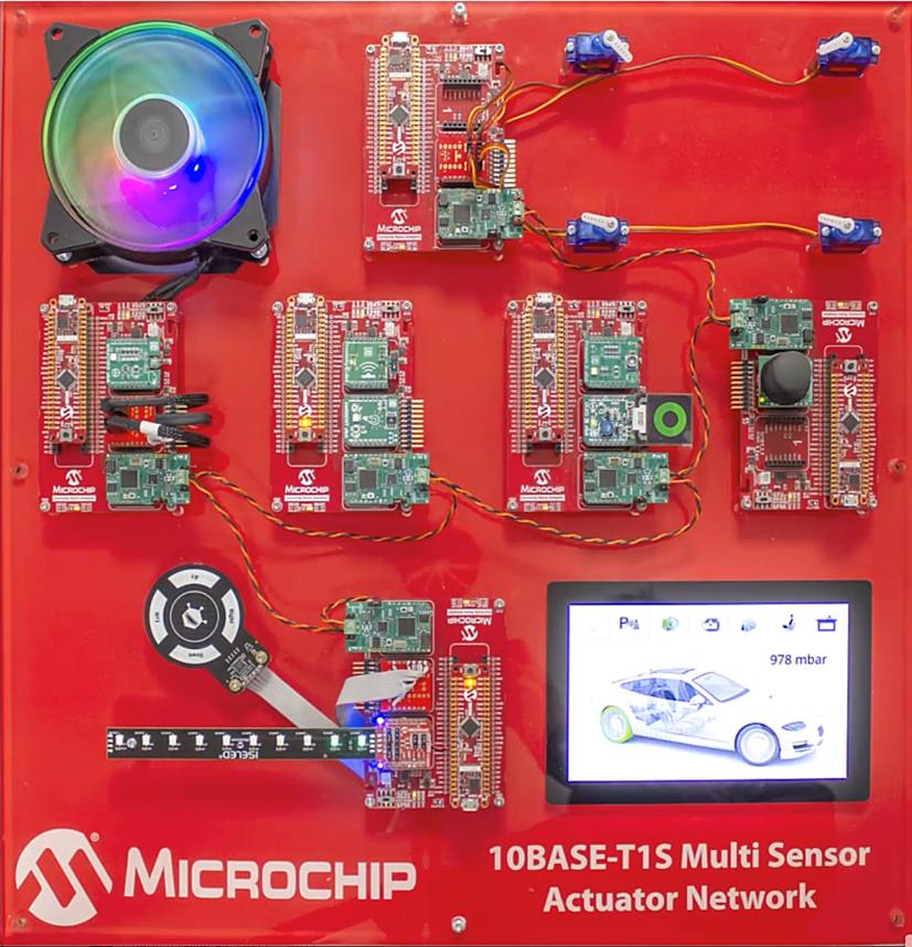
To highlight the practical benefits of 10BASET1S Ethernet, Microchip Technology developed a demonstration showcasing how this technology facilitates seamless communication between various sensors and actuators within a vehicle. The demonstration incorporates pressure, proximity, and light sensors, capturing real-world data that is processed by a centralized computing platform. The processed data then controls motors, fans, lights, and displays, creating a dynamic interaction between the digital and physical realms.
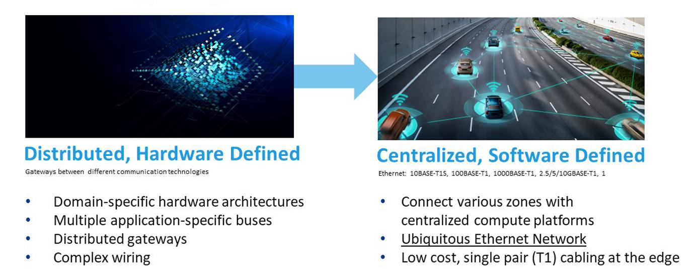
Figure 1. Networking Megatrend: From DomainSpecific to Zonal Architecture.
A video of this demonstration is available on YouTube (https://youtu.be/nD1c3eLYp7M).
Figure 3 provides a visual representation of the demonstrator setup.
This demonstration underscores the versatility of 10BASE-T1S Ethernet and its potential to simplify vehicle communication systems. By leveraging a single multidrop bus operating on a single pair of wires, the technology removes the need for dedicated Ethernet switches to connect multiple sensors and actuators. As data flows through the network, a simple switch with a 10BASET1S port can interface with higher-speed connections while preserving the standardized Ethernet frame format across the entire system.
Adopting a unified protocol for most vehicle functions presents significant advantages for automakers. Traditionally, manufacturers had to support multiple application-specific standards. Each model year introduces advancements in Advanced Driver Assistance Systems (ADAS), requiring new cameras, radar, ultrasound sensors, and, in the future, lidar. Additionally, updates to infotainment and navigation systems, along with improvements in other vehicle components, often require extensive hardware changes.
Modern vehicles may contain up to 40 different wiring harnesses, dozens or even hundreds of Electronic Control Units (ECUs), and miles of cabling that can weigh up to 250 lbs. The variety of cables necessary for different applications also creates challenges related to electromagnetic compatibility (EMC), as each application has distinct requirements.
Transitioning to a unified protocol simplifies the vehicle’s internal architecture, reducing the number of wiring harnesses and ECUs required. This, in turn, decreases weight, complexity, and associated maintenance costs while enhancing reliability and overall vehicle performance.
Upto39TOPSAIperformanceonacompactx86module
conga-TCR8

High-performance architecture withintegratedCPU, GPU,andNPU
Exceptionalmulti-purposecomputingwith upto39TOPS
Highlyefficientx86 computingwithupto8 ‚Zen4‘cores(4nm)
Superiorsinglethread performancewithupto 5.1GHz
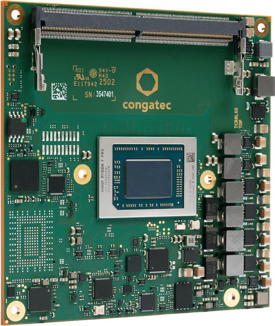

Takesyourhigh-performanceedgecomputingdesignstothenextlevel
-UniquecombinationofadvancedAI,graphics,andcomputecapabilities -Bestprice/performanceinitsclass -IdealforupgradingexistingCOMExpressapplications -10-yearlong-termavailability


Formemoryintensive applicationswithupto 128GBDDR5-5600(ECC optional) 20 YEARS
16TOPSofdedicatedAI performancewithAMD XDNA™NPU
Immersivegraphicswith RadeonRDNA3™andup to12computeunits Easydesign-inthanksto wideTDPrangefrom15W to54W

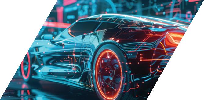
The benefits of Ethernet are not confined to the automotive industry. Industrial applications are also starting to adopt this technology, driven by the need for more efficient and scalable communication solutions. As Ethernet gains traction in sectors beyond automotive, economies of scale will help drive down costs, making it more accessible and attractive for a wider range of applications. Moreover, as knowledge about how to structure and implement Ethernet-based systems expands, it will become easier to develop and deploy these systems across various industries.
In essence, the adoption of Ethernet, and specifically 10BASE-T1S Ethernet, is a critical step in uniting the virtual and real worlds in automotive technology. This technology not only enables a future where vehicles are smarter, safer, and more interconnected than ever before but also sets the stage for broader innovation across multiple fields.
The journey of Ethernet from IT to automotive applications is a testament to the power of standardization and the potential for cross-industry collaboration to drive technological progress. As the automotive industry continues to evolve, Ethernet will play a pivotal role in shaping the vehicles of tomorrow, creating a new era of mobility defined by efficiency, security, and connectivity.
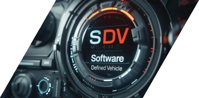
As modern vehicles evolve, they will rely on hundreds of millions of lines of code—far surpassing today’s 100 million lines. To support this growing complexity, the industry is shifting toward an Ethernet-based zonal electronic/electrical architecture. This approach consolidates sensors into a single link from the zonal gateway to the backbone and central computing platform.
The transition to an Ethernet-based zonal E/E architecture is essential for supporting the increasing complexity of modern vehicles. As the number of sensors, actuators, and electronic systems continues to grow, a scalable and efficient network infrastructure becomes critical.
Ethernet provides the bandwidth and flexibility needed to handle the vast amounts of data generated by these systems, ensuring
that the vehicle can operate smoothly and efficiently.
As the industry continues to evolve, the adoption of Ethernet-based architectures will play a crucial role in shaping the future of automotive technology, ensuring that vehicles remain connected, efficient, and innovative. What began as a concept for a unified vehicle communication architecture is now on the cusp of becoming a reality.
Some vehicles on the road today already use Ethernet for their IT architecture, and models featuring the new zonal architecture that extends to the physical-digital interface will soon enter production. This approach not only simplifies vehicle design but also opens the door to new possibilities for softwaredriven innovation, as functions that were once defined by hardware can now be implemented and updated through software.

Optimizing power consumption is crucial for battery-powered devices. With ST MEMS sensors' Machine Learning Core (MLC), decision-tree classification runs directly inside the sensor, reducing microcontroller workload and extending battery life. Discover how ST’s MEMS Studio and AIoT Craft simplify AI-powered edge computing for smarter, energy-efficient applications.
Certain ST MEMS sensors are equipped with a Machine Learning Core (MLC). This core can process input data (mostly from accelerometers, but also from gyroscopes and eventually, external data readable through the I2C interface) and make predictions using a pre-trained decision tree model. The decision tree model running directly inside the sensor can detect specific events from motion patterns with extremely low power consumption. This approach offloads the microcontroller, reduces the overall power consumption of the device, and prolongs the device’s battery runtime.
ST makes training of a decision tree more accessible through its MEMS Studio and ST
AIoT Craft applications. They both help users create machine-learning models based on decision trees for MLC-enabled sensors. The model training process is also accessible to users with little or no data science experience, thanks to the automation of most of the process.
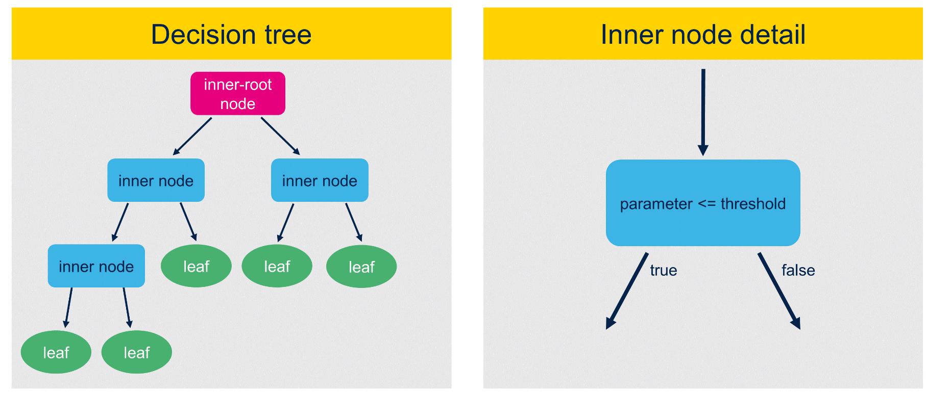
A decision tree is a supervised learning algorithm that uses a binary tree-like structure, which is also utilized in ST MEMS smart sensors. The decision tree consists of two types of nodes: inner nodes and outer nodes, along with branches. Inner nodes contain "if-then-else" conditions where a


feature calculated from input data is compared against a threshold. A specific type of inner node is the root node, which carries the initial condition to evaluate and does not have any incoming branches. Branches represent the result of the inner node (true or false) and select the next node to be evaluated. Outer nodes, also called leaf nodes, do not have any outgoing branches and contain the prediction / result.
Decision trees inside ST MEMS smart sensors can be used for a wide range of applications, including activity/fitness recognition, asset tracking, or vibration monitoring.
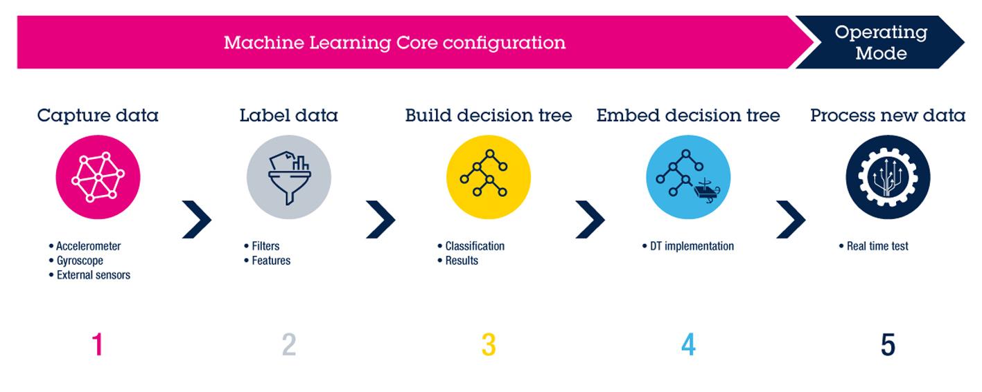
To create a decision tree, we need to:
• Define Classes: Identify the set of classes we want to predict.
• Data Collection and Labeling: Gather and tag data for each class with corresponding labels, as supervised learning requires labeled data for training.
• Data Analysis: Analyze the collected data to select useful signal features and determine the appropriate window length. Optionally, digital filters can be included.
• Feature Calculation: Calculate signal features from a specific number of samples determined by the window length. These features can include mean, variance, zero-crossing, minimum, maximum, and so on.
• Model Training: Perform model training on the selected signal features calculated from the input data.
Both MEMS Studio and ST AIoT Craft simplify the model training process, reducing the
development time. The MEMS Studio is a standalone desktop application that handles the training process locally on the user’s computer. Moreover, the application includes sensor configuration and evaluation, offline data analysis, advanced embedded features, and embedded AI development. On the other hand, the ST AIoT Craft is a web-based tool focusing on AI and IoT, where all the processing is running in the cloud, allowing more flexibility.
1. Development Board Support: The tools support several ST development boards with ready-to-use firmware for data logging and model evaluation.
2. Data Logging and Labeling: When using the ST AIoT Craft, data logging and labeling can be done using a web GUI or a companion mobile application. Data can also be imported in CSV format, for example, if logging was done using a different application like the MEMS Studio. In the MEMS Studio, it is possible to import data in CSV format, with data logging either by the MEMS Studio or a different application.
3. Data Parsing and Labeling: the ST AIoT Craft includes utilities to help parse and label large data files. Users can visualize data in a graph, select sections, and assign corresponding labels to motion patterns. The labeled dataset can then be split into smaller logs with assigned labels, ready for training. The MEMS Studio has a separate data manipulation tool with the same capabilities.
4. Automatic Analysis: The ST AIoT Craft will automatically analyze input data (selected subset of available data), select appropriate filters, features and window length. In the MEMS Studio, selected data is imported into the tool, which can be either analyzed automatically or user can manually select


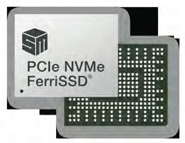


•HW&FWCustomization
•IntelligentSeries™DataProtection
•Security:AES,TCGOPAL&Pyrite

•PCIeGen4withSR-IOVTechnology
•8-Channel@1600MT/s

•DesignservicetoFAsupport
•100%screenedforlowdPPM
•ScalableprovenMPsetup


Decision trees inside ST MEMS smart sensors can be used for wide range of applications.
filters, features, and window length. It is also possible to let the tool analyze the data and then manually finetune the settings.
5. Model Training and Evaluation: The tools train a decision tree and generate a sensor configuration. The trained model can be easily evaluated using selected development boards through the web GUI or a companion mobile application in case of the ST AIoT Craft, and directly in the application when the MEMS Studio is used.
When using the ST AIoT Craft, there is no need to install any software on your PC, as your datasets and projects are stored in the cloud. This provides more flexibility when working on your application and allows an IoT system to be set up. A preconfigured Linux gateway image, running on Raspberry Pi hardware, can be downloaded from the ST AIoT Craft website.. Example projects are available for users to test the capabilities of the machine learning core.
If you want to experience the ST AIoT Craft firsthand by either trying a project example or creating your own decision tree, please visitstaiotcraft.st.com. In case a local training is preferred or you are looking for a complete all-in-one application for sensor development, get the MEMS Studio at st.com/ mems-studio. You can learn more about the sensor portfolio with machine learning core capabilities and the core itself, including application notes, onst.com/mlc.
The ST AIoT Craft and MEMS Studio are part of the ST Edge AI suite, which is a collection of software tools for integrating AI features into embedded systems – edge AI. It supports a wide range of ST products, including MEMS smart sensors, and provides resources for data handling, AI model optimization, and deployment. More information and available tools and software can be found onst.com/stedge-ai-suite.
Decision tree training flow.
Florian Drittenthaler congatec
Since their development over a decade ago, artificial neural networks have integrated into modern life, from robotics to LLMs. In AI, "inference" is a model’s ability to make decisions from live data. Using a low-power computer with an inference accelerator near the data source enhances speed, autonomy, security, and privacy.
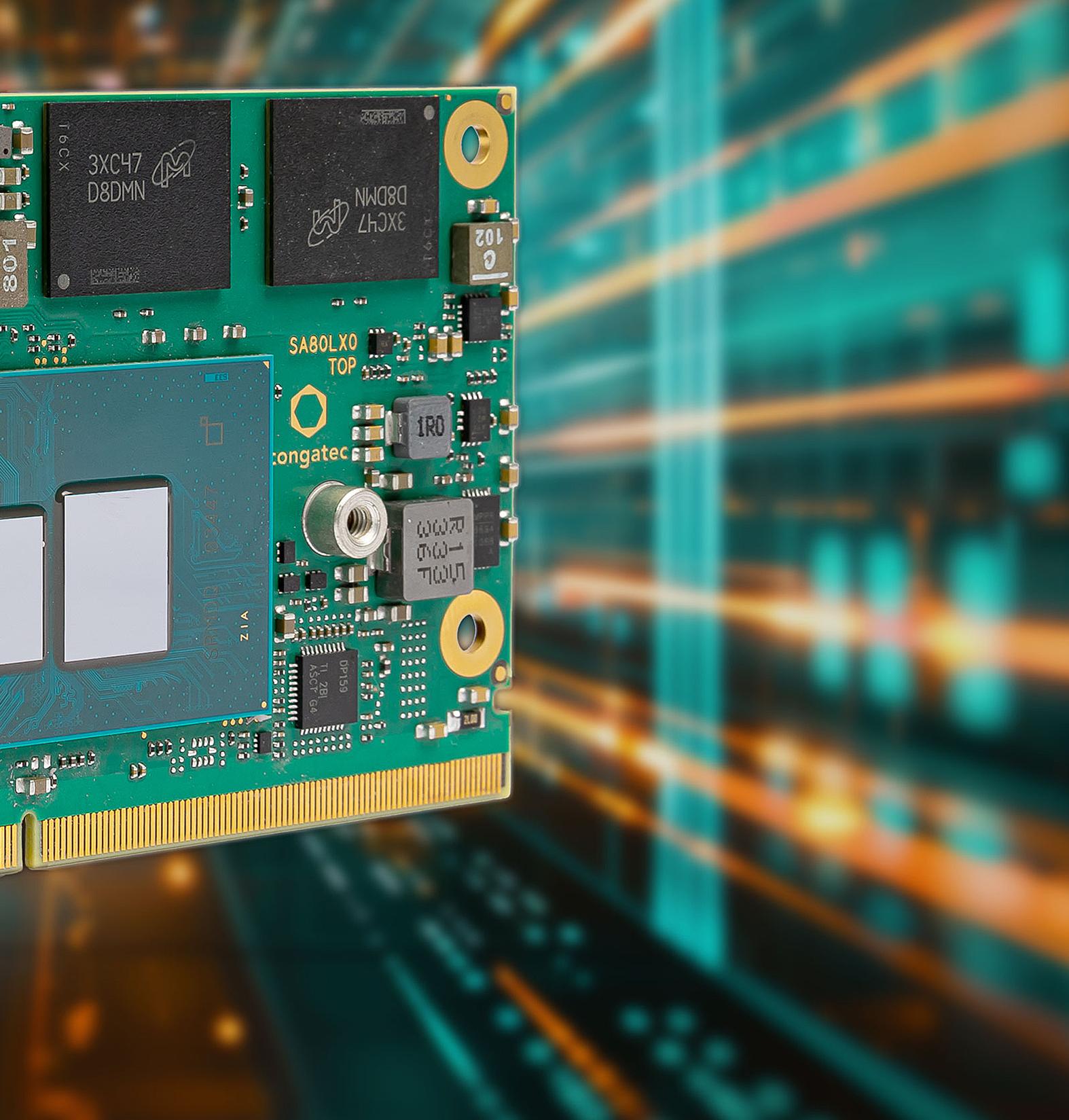
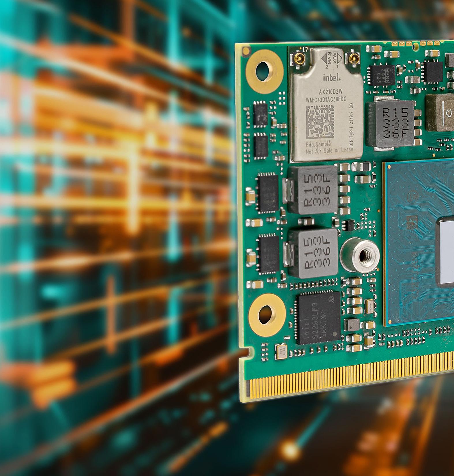
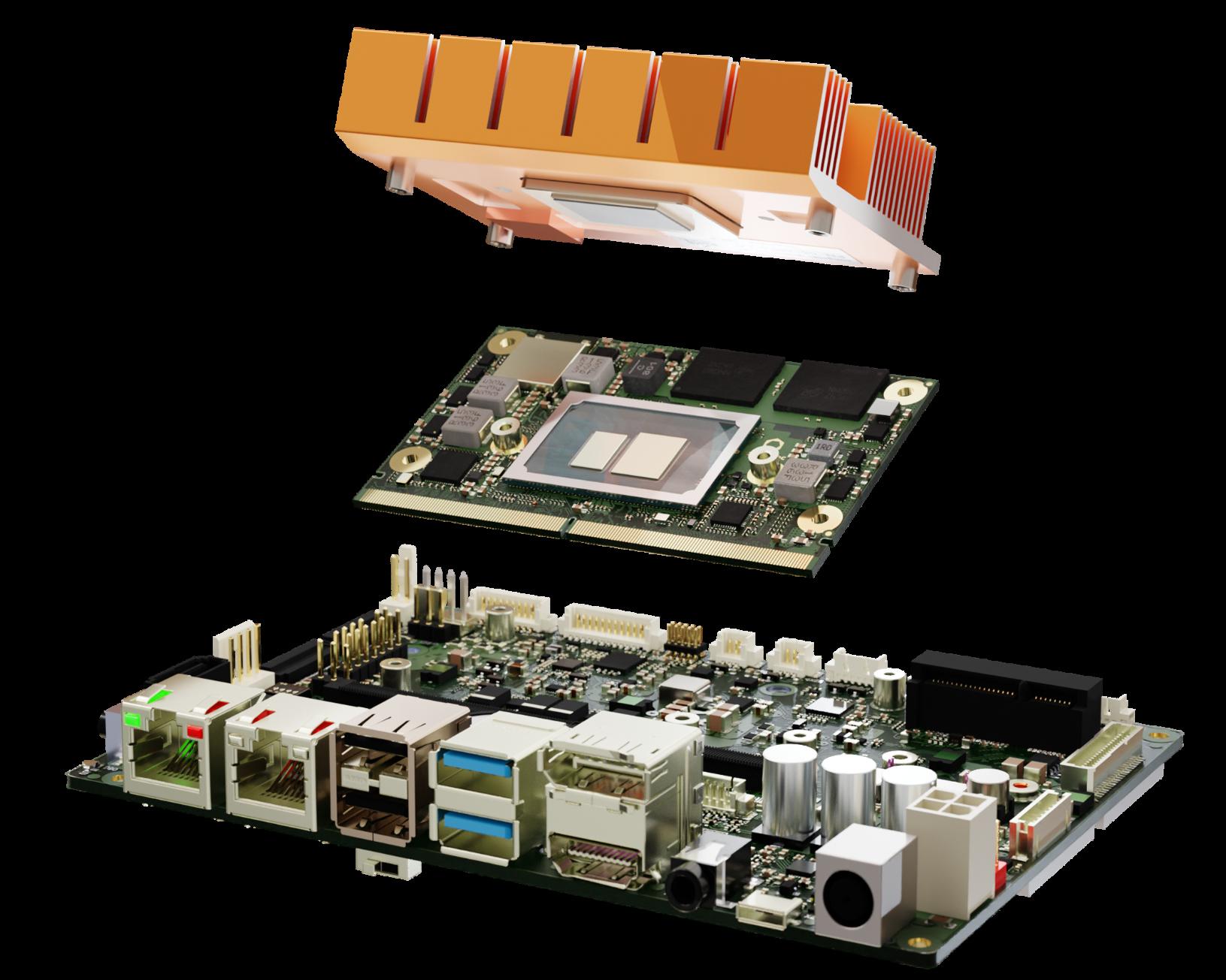
A SMARC (Smart Mobility ARChitecture) module is a compact, low-power computeron-module designed for embedded edge systems. Its small form factor, scalability, and support for advanced AI and virtualization technologies make SMARC modules ideal for industrial, medical, and IoT applications requiring energy efficiency and robust performance.
New breakthroughs are now possible for low-power computing in SMARC Computeron-Modules with Intel’s vastly improved Core i processors. The new “Amston Lake” Atom x7000RE chips can deliver superior capabilities while staying within the same power constraints, offering performance gains of up to 49% in single-threaded and 61% in multi-threaded applications [2].
Even more impressive is the 9.83-fold improvement in image classification performance, making true AI inference capabilities possible on edge and embedded computers such as SMARC modules.
Inside the Amston Lake processors, Intel now offers standardized “Gracemont” microarchitecture for its Efficient-cores (Ecores), allowing the integration of sophisticated x86 ecosystem AI features like Vector Neural Network Instructions (VNNI) in low power systems up to 15 W, which were previously reserved for systems with much higher power budgets.
The expansion of AI inference logic into lowpower systems allows industrial manufacturers to adopt smarter, more
AD2502STM32N_PRINT.pdf125/02/2519:05
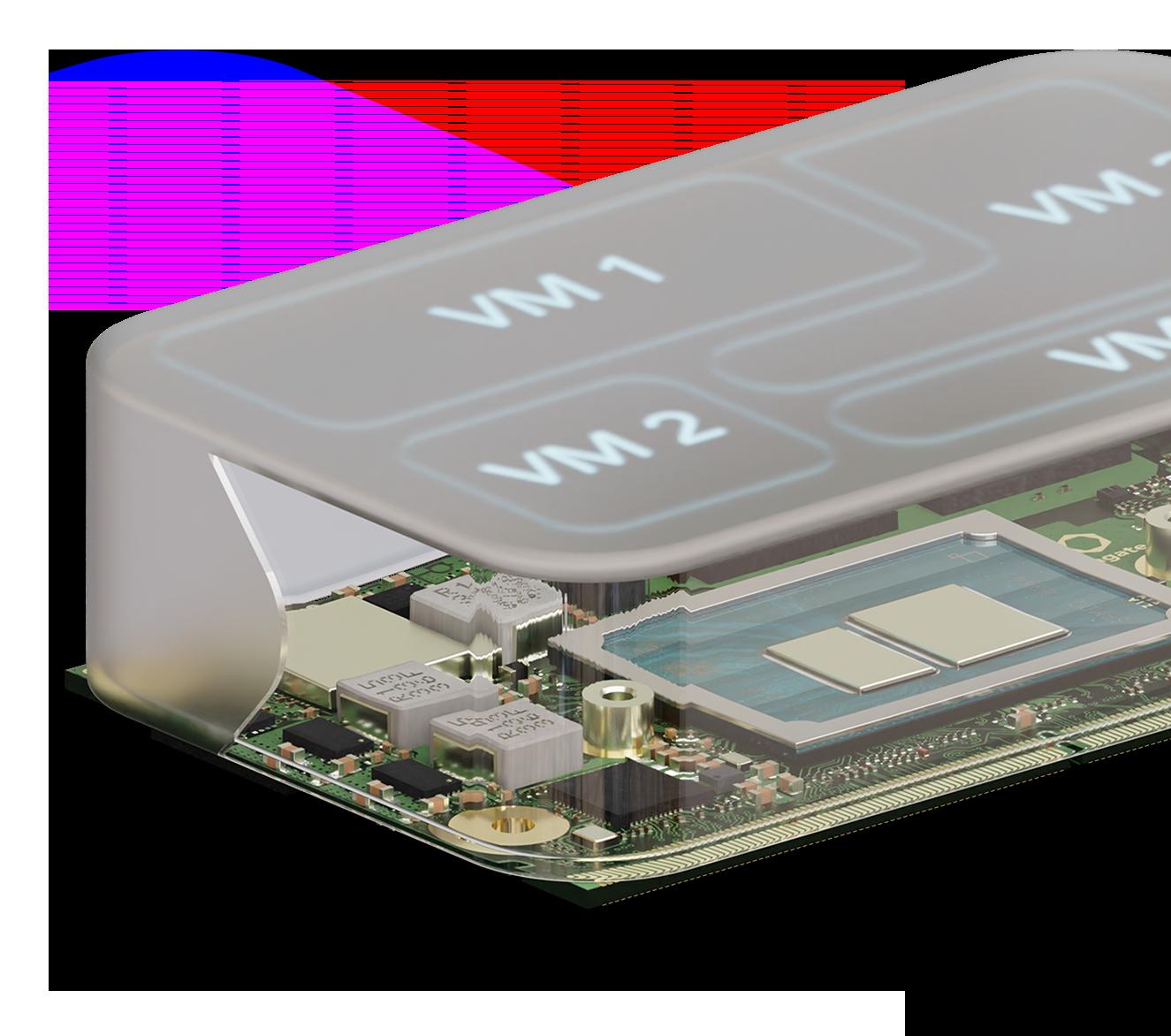
congatec’s SMARC modules come with a firmwareintegrated hypervisor, enhancing cybersecurity and simplifying virtualization.
efficient systems. AI-powered applications, including object recognition and detection, are becoming essential in improving production processes, such as in pick-and-
SMARC modules are designed with application carriers and cooling solutions, ready for series production and out-of-the-box use.
place operations or quality assurance tasks. In robotics, the ability to process visual data in real-time is essential for autonomous guided vehicles (AGVs), service robots, and collaborative robots (cobots). With the performance boost offered by the new Intel Core i processors in SMARC modules, these systems can now handle more advanced algorithms, leading to faster decision-making and safer operations.
In medical technology, advanced image segmentation and processing are driving progress in fields such as diagnostics and surgery. For instance, mobile ultrasound devices benefit from faster AI-driven processing, which can accelerate diagnosis and enhance patient outcomes. In a similar vein, AI-enhanced security systems, smart city surveillance, and even automated checkout terminals in retail environments could see significant improvements thanks to the enhanced image classification capabilities offered by these new processors.
One of the standout features of Intel’s new generation of processors is how easily developers can implement AI technologies across a broad range of applications. Developers already familiar with Intel’s AI inference logic in high-performance systems can now easily transfer that technology to compact, low-power designs with industrial temperature tolerance (-40°C to +85°C). This is because the CPUs, with up to 8 E-cores and the Intel Gen 12 UHD GPU with 32 execution units, are the same as those found in higher-end processors using the Gracemont microarchitecture, which also supports INT8 deep learning inference.
This streamlined development process is particularly valuable for applications where low power consumption and industrial temperature tolerance are critical factors. The standardization of AI-related features,
such as VNNI and AVX2 instruction sets, across Intel’s product range means that developers can focus on the unique aspects of their applications, speeding up time to market while maintaining high levels of performance and security. A full suite of tools can also be leveraged, from kernels to toolkits like OpenVino, to quickly bring AI capabilities to their systems without having to invest heavily in custom software development.
With Intel doubling the number of E-cores in the Amston Lake processors, this significantly expands the options for virtualization, a technology that offers both flexibility and security in industrial and embedded systems. By consolidating multiple systems onto a single piece of hardware, companies can reduce costs and increase efficiency while maintaining strict separation between different operational functions. This separation is crucial for enhancing cybersecurity, particularly in systems that must comply with regulations like the Cyber Resilience Act.
Virtualization also simplifies system management by allowing developers to create isolated virtual environments for tasks like maintenance or updates. This ensures that critical operations can continue running without interruption, improving both system availability and reliability. For industries relying on the Industrial Internet of Things (IIoT), the ability to run maintenance tasks on a virtual machine separate from the primary system can help reduce downtime and enhance overall system resilience.
Taking virtualization one step further, congatec has introduced a unique feature
with its Hypervisor-on-Module technology in its conga-SA8 SMARC module. By integrating a hypervisor directly into the SMARC module’s firmware, congatec simplifies the implementation of virtual machines, reducing the development burden and enabling more secure, cost-effective, and durable solutions. This feature also supports real-time capabilities, which are essential in industrial environments where precise timing and synchronization are required.
With this technology, congatec offers developers a ready-made solution for creating virtualized systems that meet the highest standards of cybersecurity and reliability. Whether the system demands realtime functionality or not, this approach provides a higher level of security compared to traditional containerization methods. Each virtual machine operates independently, creating isolated environments that prevent the spread of threats across the system.
congatec also offers an aReady.COM version of the conga-SA8, allowing customers to purchase pre-configured modules tailored to their needs. For instance, these modules can come with Bosch Rexroth’s ctrlX OS and virtual machines for tasks like real-time control, HMI, AI, IIoT data exchange, firewall, and maintenance or management functions – ready for immediate use. The new SMARC modules are also fully compatible with multiple versions of Microsoft Windows.
The conga-SA8 is among the first SMARC modules to support Wi-Fi 6E, delivering nearly triple the data rate of Wi-Fi 5 and providing more reliable connections in congested areas. It’s also ready for TSN over Wi-Fi, ensuring deterministic connections with guaranteed throughput. This offers a cost-effective alternative to 5G or Ethernet. Designed for industrial use, the module features in-band ECC for enhanced data security and soldered DRAM for greater durability in extreme environments.
The introduction of Intel Core i processors into SMARC modules marks a significant milestone for embedded and edge computing. Adopting these more powerful SMARC modules will enable new breakthroughs wherever robust, highperformance AI inference logic is needed in small, fanless systems for use in demanding industrial environments. From industrial
automation and robotics to healthcare and retail, the potential applications of this technology are vast and growing.
As AI continues to reshape industries, the ability to deploy powerful inference logic in compact, energy-efficient systems will become increasingly important. Developers now have access to an ecosystem that supports rapid implementation, allowing them to focus on innovation and differentiation.
1. SMARC 2.1 technology https://www.congatec.com/en/technologies/smarc/ 2. Compared to Intel Atom processors of the x6000RE product series. Source: https://www.intel.com/content/ www/us/en/products/details/embedded-processors/ atom/atomx7000re.html
The conga-SA8 SMARC modules from congatec come with Intel Core i3-N305 and three Intel Atom processors, offering up to 8 cores, 16 GB LPDDR5 memory (4800MT/s), and 256 GB eMMC 5.1 onboard flash. They feature Intel UHD Gen 12 graphics with 32 execution units, supporting three 4K displays. High-bandwidth connectivity options include 2.5 Gbps Ethernet, USB 3.2 Gen 2,
PCIe Gen 3, and SATA Gen 3, along with embedded I/Os like I2C, SPI, UART, and GPIOs.
These modules are compatible with operating systems such as Windows 11 IoT Enterprise, Windows 10 IoT Enterprise 2021 LTSC, and LTS Linux, making them ideal for industrial and IoT applications.
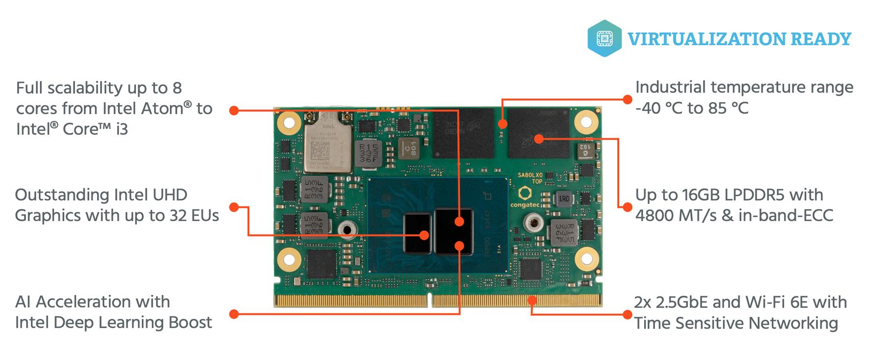
Many microcontrollers on the market provide storage density in the range of few Megabytes, which does impact the cost of the product significantly. A suitable alternative solution is using external memory, which can be purchased in volumes at comparably lower prices and with several densities’ options, typically starting from few to hundreds of Megabytes.
Nowadays, embedded systems are constantly growing their memory requirements because of increasing connectivity functionality and application-level complexity. Many microcontrollers on the market provide storage density in the range of a few Megabytes, which only a decade ago would have been regarded as more than sufficient and future-proof for the average application. On the other hand, integrating even more non-volatile memory requires quite a large silicon area, impacting the cost of the product significantly. A suitable alternative solution is using external memory, which can be purchased in volumes at
comparably lower prices and with several density options, typically starting from few to hundreds of Megabytes.
The external memory solution is suitable not only for holding application data but also for storing application code, therefore removing any concern about the supplier roadmap to be able to fulfill future needs. On the other hand, some additional aspects must be taken into consideration like the performance of the code executing from the external memory, and how to protect the application code from cloning or modification.

For the first problem, the solution is to use a memory with a wide interface which increases the physical throughput for the serial lines. Memories with an octal interface provide one of the best choices in terms of tradeoff between the number of IO connections and the achievable 2x throughput improvement compared to the legacy Quad-SPI interface. Normally such modern memories also support slightly higher operating frequencies so that the performance improvement is even more significant.
Protecting the content of the memory requires the use of cryptographic techniques to encrypt the code, since otherwise it would be easy for an attacker to connect to the memory and read out the stored information with small effort. To avoid latencies for the decryption process it is necessary to use design solutions that are fast and executed in line with the instruction fetching process—in other words, transparent from the CPU perspective.
The latest Renesas MCUs like the RA8x1 series implement a so-called ‘decryption on the fly’ (DOTF) architecture which serves exactly this purpose. A conceptual representation of the solution can be seen in Figure 1.
The principle is quite simple and based on the AES encryption/decryption standard, using counter mode (CTR) as specified in NIST SP800-38A. The principle of CTR mode operation is shown in Figure 2.
In CTR mode, a set of counters are used as input to a block cipher function, to generate a secret output which is then exclusive-ORed with the plaintext (or ciphertext) to encrypt (or decrypt) the message data. The sequence of counters must be chosen so that every input block in the set is unique. This requirement is valid for all ‘messages’ (i.e. data items) which are encrypted using the same key.
One nice property of CTR mode is that the cipher functions associated with the counter can be performed upfront independently from each other, and do not need to wait for the data block to be available. This helps to reduce latency while reading out the encrypted data from the octa memory, since the generation of the output block can be done in parallel. Also, a certain plaintext block can be recovered independently from any other block, which is convenient for fetching program data, since depending on the program flow the processor might request to read code at non-sequential address locations.
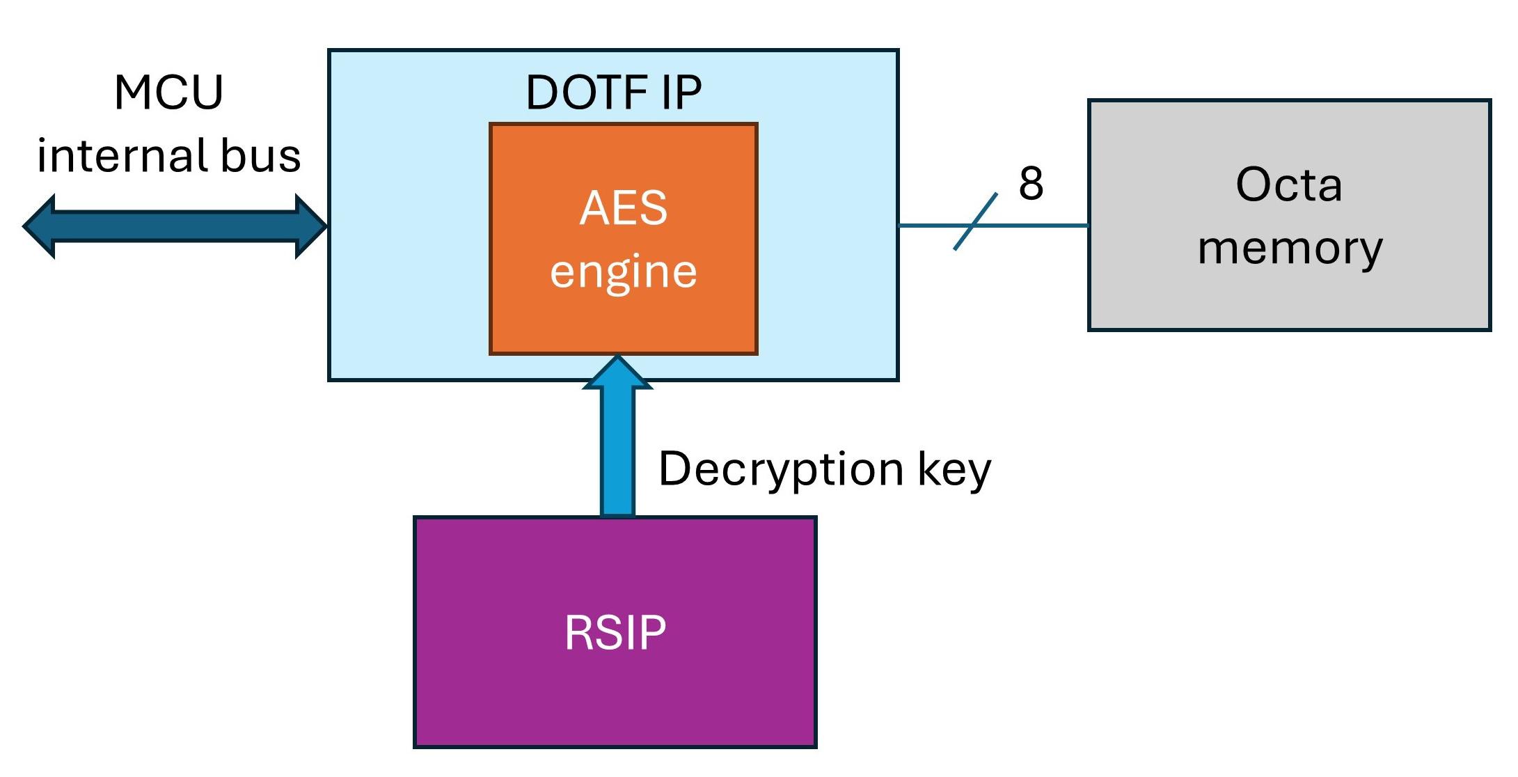
Figure 1. DOTF architecture.
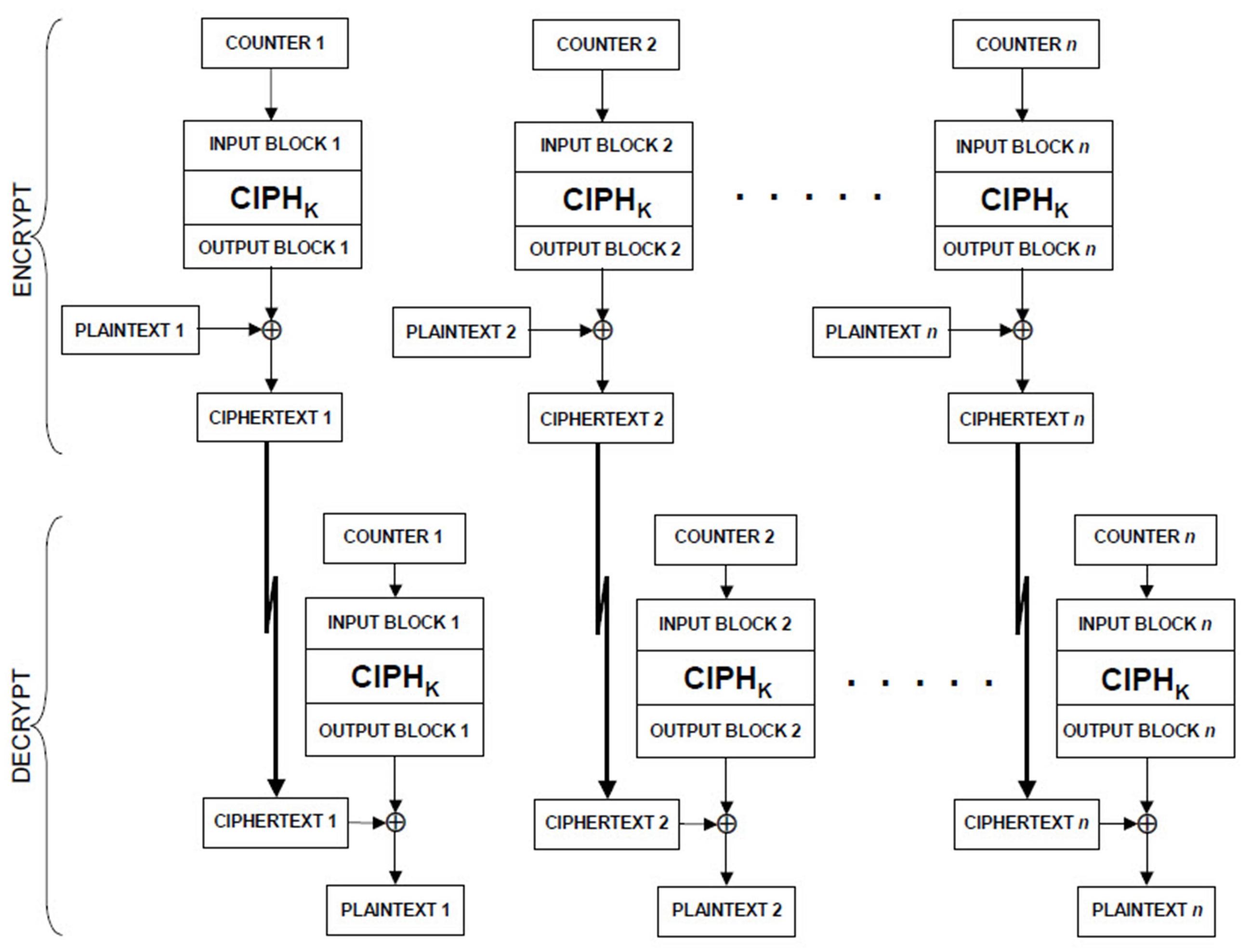
The parameters used to define the counters need to be chosen carefully to ensure their uniqueness. An AES block is 16 bytes (128 bits) in size; therefore, the counter must be also 128 bits wide. Every encrypted block in memory is aligned to 16 bytes too, and to create a unique counter a concatenation of an initial value and the memory address can be used.
The initial value is essentially a nonce (unique, random number used once) and the address of the encrypted block being read has the 4 LSBs masked, to create the counter value according to the following scheme: counter [127:0] = InitialValue [127:28] || (MemoryAddress [31:4] >> 4).
There are a couple of further interesting features in the implementation which are very useful to make it a flexible and user-
friendly solution. First, the application can define an address boundary for which the decryption on the fly will be used, or otherwise bypassed, as shown in Figure 3.
This makes it very convenient if the application wants to partition the flash contents between code and other data, where the code gets decrypted on the fly and the data gets simply read without decrypting. The latter also allows the application to use another key or encryption mode for the data and avoids sharing the application code encryption/decryption key for multiple purposes.
As for the alignment of the DOTF area, even though the AES encryption standard implies a minimum alignment of 16 bytes. Given the typical organization of a flash memory, the boundary should rather be placed on a sector
or block size (the minimum flash unit size which can be erased while programming). In the implementation, the DOTF boundary is configurable to 4KB address alignment; in fact the application shall anyway avoid having a memory block storing both DOTF and non-DOTF data, which would make infield-updates and factory programming unnecessarily complicated.
The flash memory device is mapped linearly into the addressable space of the MCU, and the Octa IP takes care of issuing the appropriate read commands, this is typically called XiP (execute-in-place) operation mode. For the encrypted area any access to the requested 16-byte blocks can be done efficiently by issuing one time the required address, and then reading the data continuously, thereby reducing the OctaSPI protocol overhead to a minimum.
Another important aspect is how the decryption key is handled and loaded. In devices supporting DOTF, there is a dedicated AES engine implemented within the IP but the key for the decryption process gets loaded over a private bus connection to the Renesas secure IP; this avoids leaking the key value over the internal MCU bus interconnect. Additionally, the keys handled by the Renesas secure IP are themselves encrypted, so these can be stored safely in memory without confidentiality and integrity concerns.
The DOTF engine supports 128-, 192- and 256-bit size keys for maximum flexibility and future-proof choices, and there is no limit on the number of different keys which can be used to decrypt a specific image. The latter implies that any firmware update can use a different key if desired, and there is no need to share the same key between different MCUs. Preparing the new image can be conveniently done offline on a secure host, before sending the image update to a device in the field or sending the encrypted image to a contract manufacturer for programming.
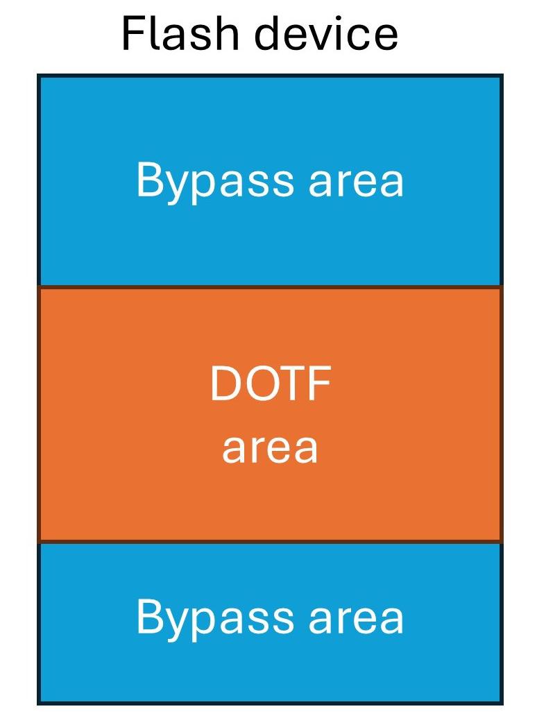
The initial decryption key, or a “key update key” (for updating the decryption key in the field) can be injected securely in the MCU during production. Injected keys, whether in the field or at production stage, are always bound to the specific MCU, so that cloning is prevented.
Furthermore, the IP provides countermeasures to protect against side channel attacks. All runtime operation is performed transparently by the hardware, and the provided software drivers take care to initialize and load the parameters for the DOTF operation (initial value, boundaries) and the key, before operation can start.
All MCUs which require memory expandability and complex application requirements will benefit from such kind of solution, which ensures that the MCU developer will benefit from a solid application roadmap while also protecting the software investment.
For more information on the RA MCU family, please visit www.renesas.com/ra

Solid-state drives bring inherently high reliability to applications from entrylevel consumer equipment to mission-critical systems. Proper data protection mechanisms can maximise the lifetime of the drive by taking preventative measures when needed.
Solid-state drives (SSDs) provide high-performing and compact mass storage for embedded computing applications that make today’s digital lifestyles possible. They are found in equipment such as car computing and navigation systems, thin clients, point-of-sale terminals, multifunction printers, telecommunications equipment, factory automation tools, and server systems of all types and sizes from small data centres to cloud-level.
The typical SSD lifetime is heavily dependent on the NAND Flash technology used. QLC (quad-level cell) and TLC (triple-level cell) NAND have a lifetime between 1,000 to 3,000 program/erase cycles per cell, while the expected lifetime for MLC (multi-level cell) is 3,000 to 10,000 cycles. SLC (single-level cell) NAND has the longest lifetime, up to 100,000 cycles. These known limitations help system designers choose the optimum SSD technology for their
application, depending on the required endurance, price, and mission criticality. TLC NAND, with the lowest endurance, typically comes at a lower price than the others and is usually sought for use in costconscious consumer products.
Although the typical lifetime range for any given technology can be predicted, the actual lifetime of any given drive cannot be known. Unexpected failure can cause data loss, system downtime, and repair costs. The consequences can range from inconvenient to catastrophic. System designers need tools that can help avoid these problems by managing and protecting the SSD to maximise its lifetime and taking preventative measures before any drive failure occurs.
A failing SSD can significantly degrade system performance. Slow read/write speeds, increased

access times, and frequent error handling can lead to a sluggish response and decreased overall system efficiency.
After failure, recovery and repair can involve replacing the faulty SSD, restoring data from backups, and reconfiguring the system, all of which can be time-consuming and result in additional costs. Professional assistance may be needed to diagnose and resolve the issue. In some cases, the entire embedded system might need to be replaced if the SSD failure cannot be easily rectified.
To mitigate the consequences of SSD failure, it is essential to have proper backup strategies, redundancy measures, and monitoring systems in place.
Among the tools available for managing SSDs safely and securely, built-in data protection mechanisms can both prevent and mitigate expected lifetime-based failures. Additionally, they can provide protection
against hazards such as prolonged duration, excessive read access, temperature fluctuations, overtemperature, power instability, hacking,, all of which can shorten the life of the drive.
FerriSSDs come with a set of intelligent data protection mechanisms that meet the storage needs of different application systems and can be effectively activated in various environments where data loss may occur.
These mechanisms include IntelligentLog, which comprehensively records the health status of the SSD to let system developers understand its current condition and take appropriate measures (see picture below). When the SSD approaches its usage limit, it is possible to proactively inform the host of any potential danger,. In terms of read and write cycles, data migration is initiated to ensure data integrity and prevent any loss. It also records major event logs for faster and more efficient debugging. In addition, IntelligentScan performs automatic scanning and repairs, ensuring that data stored in the
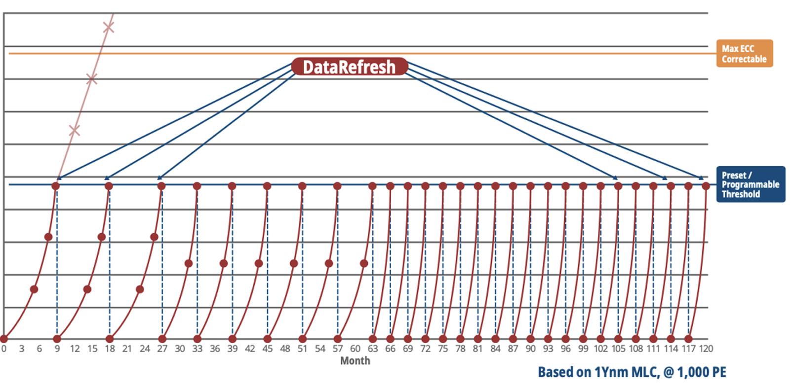
secure area can be read and written to correctly. It increases the duration of data storage and extends the lifespan of the SSD (see figure 1).
OVERTEMPERATURE PROTECTION
Exposure to high temperatures can present a number of hazards to SSDs, including accelerating the degradation of the NAND flash memory cells, which over time, can shorten the lifespan of the drive. Excessive heat can also affect the integrity of the
stored data and increase the risk of read or write errors. Performance degradation can also occur, including slower access times, decreased transfer rates, and latency issues, resulting in decreased overall system performance and responsiveness.
To prevent such problems, FerriSSD IntelligentThermalTM monitors the drive’s temperature and activates cooling mechanisms if a certain threshold is exceeded. It effectively chooses between host-controlled thermal management
Figure 1. IntelligentScan & DataRefresh functions can detect highrisk factors before the data is lost.
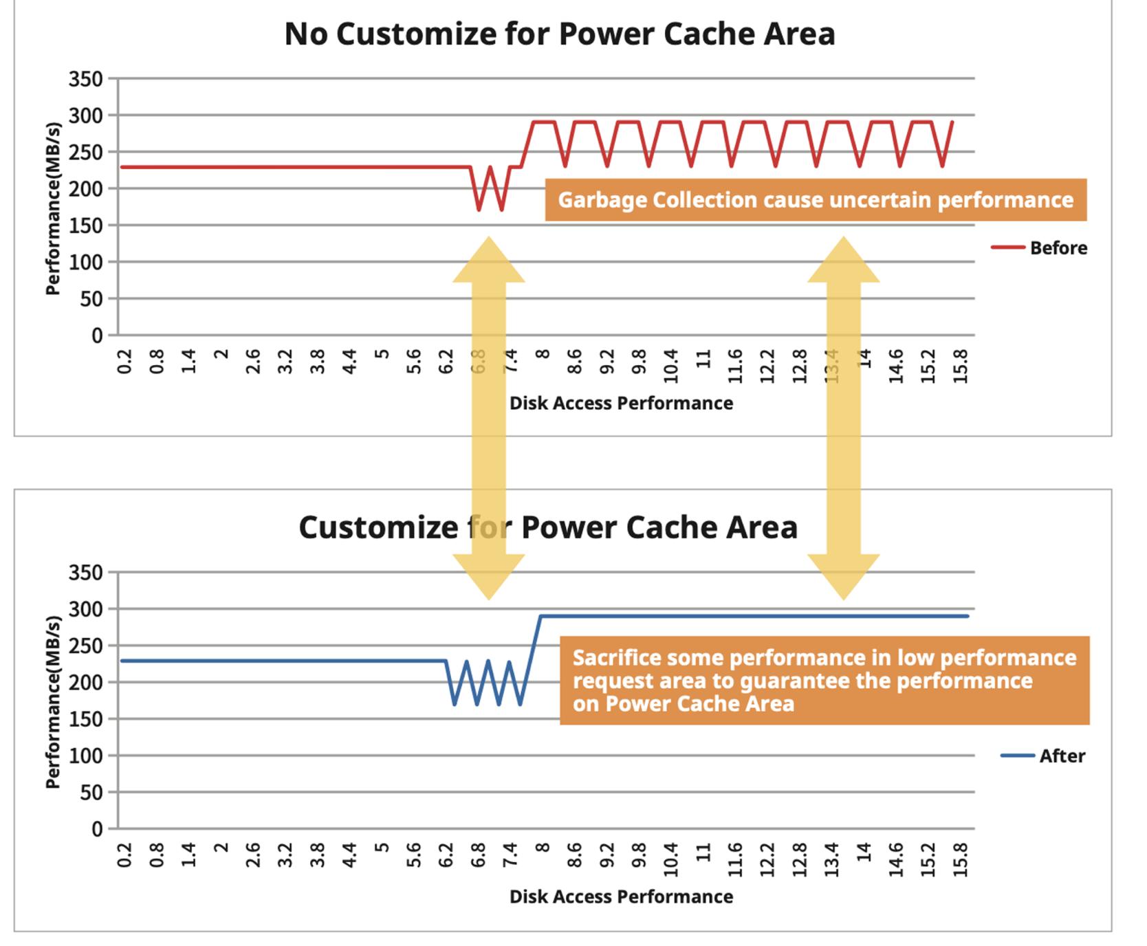
Figure 2. IntelligentFlus h enables instant data migration at a consistent speed, alowing data top be swiftly moved to a secure storage block.
(HCTM) and drive-controlled thermal management (DCTM) to control temperature and prevent SSD damage in hightemperature conditions.
Power loss can affect data protection in several ways. If power is suddenly lost during a write operation, the SSD may not have enough time to complete the data writing process. This can result in partially written data or metadata inconsistencies, causing the stored information to be corrupted or inaccessible. Also, power loss during remapping processes such as wear levelling, which is performed regularly to distribute write operations across memory cells evenly, can lead to data mapping errors or incorrect tracking of data locations. This can cause data loss or fragmentation, affecting the overall reliability and accessibility of the stored data.
In addition, data temporarily stored in cache can be lost if a power outage occurs before the cached data is written into the main storage, resulting in data inconsistencies or file system corruption. Also, power loss can interrupt the updating or synchronization of metadata used for organising and managing the stored data, leading to corruption or inconsistencies that can cause issues during boot-up or result in the loss of file system integrity.
To protect against power disruptions, FerriSSD IntelligentShieldTM ensures that all data being transmitted is securely stored in a designated safe area, preventing data loss caused by power outages. The drive initiates this mechanism as soon as instability in the power supply is detected and also activates FerriSSD’s IntelligentFlushTM. This enables instant data migration at a consistent speed, allowing data to be swiftly moved to a secure storage block (see figure 2).
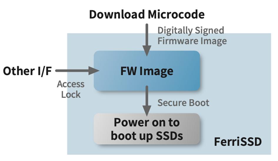
Figure 3. IntelliGuard technology maintainsa boot security by enhancing authentication and protection mechanisms of the SSD´ s firmware.
The data protection features also include preventing cyberattacks that could compromise the SSD's management functionality. Because all data transmission and protection mechanisms within the SSD are managed by the firmware, safeguarding them against attacks is critical. Ferri’s IntelligentGuard technology achieves this by enhancing authentication and protection mechanisms of the SSD's firmware (see figure 3).
Additional features include IntelligentImage, a preloading mechanism for embedded systems that allows data to be loaded onto a secure block prior to surface mounting assembly. This protects the data against manufacturing hazards such as damage by high reflow soldering temperatures and significantly enhances production line efficiency.
Finally, IntelligentZones supports a multiName Space design, allowing the SSD to be tailored according to the requirements of different system designers. The SSD is divided into different storage blocks, and data is placed in the appropriate block based on the design. This ensures data integrity as well as effective utilization of SSD capacity, thereby enhancing economic efficiency.
Doug Bailey Power Integrations
SiC v GaN v SJ MOSFETs v IGBTs? Each has its place and that’s why we, at Power Integrations, do not treat GaN as a market, it’s a technology. It’s just one of many in our armoury, along with SiC and various different MOSFET technologies and we use what we determine to be the most appropriate, application by application.
The perception of GaN’s place has changed significantly with our recent dramatic launch of a GaN device – and I think that is a justifiable adjective to use – with a breakdown voltage of 1700 V. Let’s put that into perspective: 1700 V is 450 V higher than our previous best, and 70% higher than the best offered by any other maker (which, incidentally, we believe is currently not
available as a shippable high-volume product). Most GaN companies are struggling to get much above 750 V. We launched a flyback power supply IC, InnoMux-2, that is rated at 1700 V, so it can easily cope with 1000 VDC rail applications. It is available to order with a 16-week delivery lead time in volume, and samples are available off the shelf.

What does this mean for industry and the whole ‘GaN v SiC, which power IC technology is best’ discussion?
In short, we believe that GaN will soon be able to address all application sectors from the low 10s of watts up to 100s of kilowatts.
Let’s break it down. GaN has already won the low power charger market from 30 W to, say, 240 W. This is because it is much more efficient than Super junction MOSFETs, featuring negligible switching losses and very low specific RDSON. Therefore, higher power densities are achievable, devices can be made smaller or more powerful, and the thermal management challenge is much reduced. Although MOSFETs are currently cheaper than GaN HEMTs, the need for advanced resonant topologies and heatsinks makes them less cost-effective than GaN at the system level. This GaN advantage will only improve as economies of scale kick in and production ramps up. The only reason why MOSFETs may be preferred for very low power applications (for example <20 W) is that the GaN die at low power levels are so small they are hard to handle.
As we move up in power levels through 500 W, 1 kW and up to 10kW, GaN is also winning.
Here we are looking at applications such as refrigerators, e-bike chargers, washing machines and other white goods, HVAC compressors, solar, certain automotive functions such as the on-board charger and lead-acid replacement battery circuits, and server PSUs. All these are transitioning from MOSFETs. Some have already made the move to SiC, and since SiC and GaN have comparable efficiency ratings, why should GaN prevail here? Simply, the reason is cost. SiC requires huge amounts of energy to create the high processing temperatures required. GaN does not. A GaN device is inherently no more expensive to produce than a silicon part – devices can even be made on the same production lines with relatively few modifications.
More and more of these 1 to 10kW applications – previously the preserve of MOSFETs and SiC - will be addressable by GaN, and it won’t stop there. Currently, GaN tops out at around 7-10 kW. That’s a little short of satisfying the needs of the EV inverter market – the biggest single power IC application TAM – but you only need another factor of 10 to get to EV power levels of a few hundred kW, and a factor of 10 in high tech is a matter of just a few years. There's no substantive constraint, there's no physical
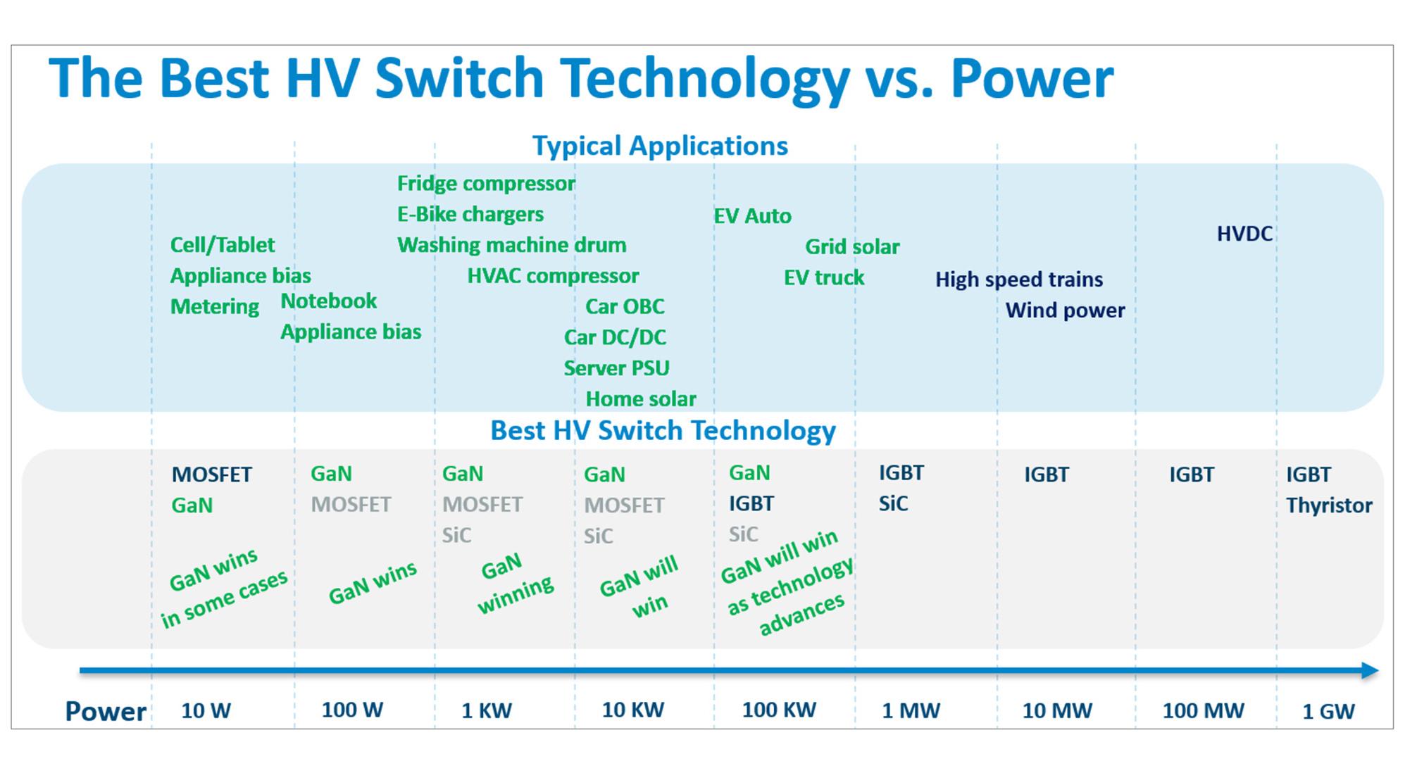
limitation…it’s not invention or inspiration that is needed, it's development.
At the very high power end of the scale - multi-megawatt wind turbines and gigawatt high-voltage DC installations - IGBTs are well established and comparatively cheap. Therefore, SiC looks set to be squeezed into a relatively small section of the market, which needs the higher currents that the vertical technology can offer.

More and more of these 1 to 10kW applications will be addressable by GaN, and it won’t stop there, says Doug
One final point. When any new technology comes along, or takes a significant step forward, the first thing it
AD2502STM32WBA6_PRINT.pdf125/02/2519:09
does it to directly replace the previous tech. But then someone bright comes along and says,‘well that’s OK, but the new tech allows us to completely rethink the design – to come up with a new concept that makes best use of the new technology without referring back to what was required by the old’. We’re continuing to innovate at the microelectronics, packaging, system, and algorithm levels to develop application-specific power products that advance efficiency, cost-effectiveness, and component count, opening up new ideas for new markets.

•Arm®Cortex®-M33at100MHz
•Multiprotocolsupport:Bluetooth®LowEnergy5.4,Zigbee, OpenThread,Matter(end-devices)
•Upto2Mbytesflashand512KbytesRAM
•Richecosystemofferinghardware,embeddedsoftware&tools,documentation
•SESIPLevel3targetcertification:compliancewiththeUSCyberTrustMark andtheEURadioEquipmentDirective(RED)
•10yearslongevitycommitment
www.st.com/stm32wba6
The world of embedded solutions is expanding rapidly, but navigating the best way to find them can be a challenge. What is the right approach for your project? What is the relationship between component suppliers and distributors?
At ECF25 – Embedded & distribution, we’re here to provide insights and solutions to these crucial questions. The event is designed for electronics designers seeking the latest advancements, corporate buyers aiming to streamline their supply chains, business leaders driving innovation in their companies, and anyone passionate about embedded electronics!
As always, the event is free for visitors. We´ll hear keynote speeches and technical presentations from your experts.
Join us at ECF25 – Embedded & distribution
Date: Wednesday, June 4, 2025
Location: Maria 01, Helsinki
For more information see www.embeddedconference.fi
To book a place or ask for sponsor packages please contact
ETN editor-in-chief Veijo Ojanperä
vo@etn.fi +358-407072530 or Sales manager Rainer Raitasuo
+46-734171099
rr@etn.se
ETNdigi is a specialized digital magazine from ETN. We cover components, test & measurement, radios & networks, and the entire scope of embedded software. To put it simply: everything related to electronics and embedded design.
Want to join us? Just contact ETN editor-in-chief Veijo Ojanperä at vo@etn.fi or our sales manager Rainer Raitasuo at rr@etn.se. More info about the pricing can be found at etn.fi/advertise.