WoodheadPublishingSeriesinElectronic andOpticalMaterials
1 Circuitanalysis
J.E.Whitehouse
2 Signalprocessinginelectroniccommunications:Forengineersand mathematicians
M.J.Chapman,D.P.GoodallandN.C.Steele
3 Patternrecognitionandimageprocessing
D.Luo
4 Digital filtersandsignalprocessinginelectronicengineering:Theory, applications,architecture,code
S.M.BozicandR.J.Chance
5 Cableengineeringforlocalareanetworks
B.J.Elliott
6 DesigningastructuredcablingsystemtoISO11801:Cross-referenced toEuropeanCENELECandAmericanStandards
Secondedition
B.J.Elliott
7 Microscopytechniquesformaterialsscience
A.ClarkeandC.Eberhardt
8 Materialsforenergyconversiondevices
EditedbyC.C.Sorrell,J.NowotnyandS.Sugihara
9 Digitalimageprocessing:Mathematicalandcomputationalmethods
Secondedition
J.M.Blackledge
10 Nanolithographyandpatterningtechniquesinmicroelectronics
EditedbyD.Bucknall
11 Digitalsignalprocessing:Mathematicalandcomputationalmethods, softwaredevelopmentandapplications
Secondedition
J.M.Blackledge
12 Handbookofadvanceddielectric,piezoelectricandferroelectricmaterials: Synthesis,propertiesandapplications
EditedbyZ.-G.Ye
13 Materialsforfuelcells
EditedbyM.Gasik
14 Solid-statehydrogenstorage:Materialsandchemistry
EditedbyG.Walker
15 Lasercoolingofsolids
S.V.PetrushkinandV.V.Samartsev
Polymerelectrolytes:Fundamentalsandapplications
EditedbyC.A.C.SequeiraandD.A.F.Santos
17 Advancedpiezoelectricmaterials:Scienceandtechnology
EditedbyK.Uchino
18 Opticalswitches:Materialsanddesign
EditedbyS.J.ChuaandB.Li
19 Advancedadhesivesinelectronics:Materials,propertiesandapplications
EditedbyM.O.AlamandC.Bailey
20 Thin filmgrowth:Physics,materialsscienceandapplications
EditedbyZ.Cao
21 Electromigrationinthin filmsandelectronicdevices:Materialsandreliability
EditedbyC.-U.Kim
22 Insitu characterizationofthin filmgrowth
EditedbyG.KosterandG.Rijnders
23 Silicon-germanium(SiGe)nanostructures:Production,propertiesand applicationsinelectronics
EditedbyY.ShirakiandN.Usami
24 High-temperaturesuperconductors
EditedbyX.G.Qiu
25 Introductiontothephysicsofnanoelectronics
S.G.TanandM.B.A.Jalil
26 Printed films:Materialsscienceandapplicationsinsensors,electronics andphotonics
EditedbyM.PrudenziatiandJ.Hormadaly
27 Lasergrowthandprocessingofphotonicdevices
EditedbyN.A.Vainos
28 Quantumopticswithsemiconductornanostructures
EditedbyF.Jahnke
29 Ultrasonictransducers:Materialsanddesignforsensors,actuators andmedicalapplications
EditedbyK.Nakamura
30 Wasteelectricalandelectronicequipment(WEEE)handbook
EditedbyV.GoodshipandA.Stevels
31 ApplicationsofATILAFEMsoftwaretosmartmaterials:Casestudies indesigningdevices
EditedbyK.UchinoandJ.-C.Debus
32 MEMSforautomotiveandaerospaceapplications
EditedbyM.KraftandN.M.White
33 Semiconductorlasers:Fundamentalsandapplications
EditedbyA.BaranovandE.Tournie
34 Handbookofterahertztechnologyforimaging,sensingandcommunications
EditedbyD.Saeedkia
35 Handbookofsolid-statelasers:Materials,systemsandapplications
EditedbyB.DenkerandE.Shklovsky
36 Organiclight-emittingdiodes(OLEDs):Materials,devicesandapplications
EditedbyA.Buckley
37 Lasersformedicalapplications:Diagnostics,therapyandsurgery
EditedbyH.Jelínkova
16
xii WoodheadPublishingSeriesinElectronicandOpticalMaterials
Semiconductorgassensors
EditedbyR.JaanisoandO.K.Tan
39 Handbookoforganicmaterialsforopticaland(opto)electronicdevices:Properties andapplications
EditedbyO.Ostroverkhova
40 Metallic filmsforelectronic,opticalandmagneticapplications:Structure, processingandproperties
EditedbyK.BarmakandK.Coffey
41 Handbookoflaserweldingtechnologies
EditedbyS.Katayama
42 Nanolithography:Theartoffabricatingnanoelectronicandnanophotonicdevices andsystems
EditedbyM.Feldman
43 Laserspectroscopyforsensing:Fundamentals,techniquesandapplications
EditedbyM.Baudelet
44 Chalcogenideglasses:Preparation,propertiesandapplications
EditedbyJ.-L.AdamandX.Zhang
45 HandbookofMEMSforwirelessandmobileapplications
EditedbyD.Uttamchandani
46 Subseaopticsandimaging
EditedbyJ.WatsonandO.Zielinski
47 Carbonnanotubesandgrapheneforphotonicapplications
EditedbyS.Yamashita,Y.SaitoandJ.H.Choi
48 Opticalbiomimetics:Materialsandapplications
EditedbyM.Large
49 Opticalthin filmsandcoatings
EditedbyA.PiegariandF.Flory
50 Computerdesignofdiffractiveoptics
EditedbyV.A.Soifer
51 SmartsensorsandMEMS:Intelligentdevicesandmicrosystemsforindustrial applications
EditedbyS.NihtianovandA.Luque
52 Fundamentalsoffemtosecondoptics
S.A.KozlovandV.V.Samartsev
53 Nanostructuredsemiconductoroxidesforthenextgenerationofelectronics andfunctionaldevices:Propertiesandapplications
S.Zhuiykov
54 Nitridesemiconductorlight-emittingdiodes(LEDs):Materials,technologies andapplications
EditedbyJ.J.Huang,H.C.KuoandS.C.Shen
55 Sensortechnologiesforcivilinfrastructures
Volume1:Sensinghardwareanddatacollectionmethodsforperformance assessment
EditedbyM.Wang,J.LynchandH.Sohn
56 Sensortechnologiesforcivilinfrastructures
Volume2:Applicationsinstructuralhealthmonitoring
EditedbyM.Wang,J.LynchandH.Sohn
57 Graphene:Properties,preparation,characterisationanddevices
EditedbyV.SkakalovaandA.B.Kaiser
38
WoodheadPublishingSeriesinElectronicandOpticalMaterials xiii
58 Silicon-on-insulator(SOI)technology
EditedbyO.KononchukandB.-Y.Nguyen
59 Biologicalidentification:DNAamplificationandsequencing,optical sensing,lab-on-chipandportablesystems
EditedbyR.P.Schaudies
60 Highperformancesiliconimaging:FundamentalsandapplicationsofCMOS andCCDsensors
EditedbyD.Durini
61 Nanosensorsforchemicalandbiologicalapplications:Sensingwith nanotubes,nanowiresandnanoparticles
EditedbyK.C.Honeychurch
62 Compositemagnetoelectrics:Materials,structures,andapplications
G.Srinivasan,S.PriyaandN.Sun
63 Quantuminformationprocessingwithdiamond:Principlesandapplications
EditedbyS.PrawerandI.Aharonovich
64 Advancesinnon-volatilememoryandstoragetechnology
EditedbyY.Nishi
65 Lasersurfaceengineering:Processesandapplications
EditedbyJ.Lawrence,C.Dowding,D.WaughandJ.Griffiths
66 Powerultrasonics:Applicationsofhigh-intensityultrasound
EditedbyJ.A.Gallego-JuarezandK.F.Graff
67 Advancesindelay-tolerantnetworks(DTNs):Architectures,routingand challenges
EditedbyJ.J.P.C.Rodrigues
68 Handbookof flexibleorganicelectronics:Materials,manufacturingand applications
EditedbyS.Logothetidis
69 Machine-to-machine(M2M)communications:Architecture,performanceand applications
EditedbyC.Anton-HaroandM.Dohler
70 Ecologicaldesignofsmarthomenetworks:Technologies,socialimpactand sustainability
EditedbyN.SaitoandD.Menga
71 Industrialtomography:Systemsandapplications
EditedbyM.Wang
72 Vehicularcommunicationsandnetworks:Architectures,protocols,operation anddeployment
EditedbyW.Chen
73 Modeling,characterizationandproductionofnanomaterials:Electronics, photonicsandenergyapplications
EditedbyV.TewaryandY.Zhang
74 Reliabilitycharacterisationofelectricalandelectronicsystems
EditedbyJ.Swingler
75 Industrialwirelesssensornetworks:Monitoring,controlandautomation
EditedbyR.BudampatiandS.Kolavennu
76 Epitaxialgrowthofcomplexmetaloxides
EditedbyG.Koster,M.HuijbenandG.Rijnders
77 Semiconductornanowires:Materials,synthesis,characterizationandapplications
EditedbyJ.ArbiolandQ.Xiong
xiv WoodheadPublishingSeriesinElectronicandOpticalMaterials
78 Superconductorsinthepowergrid
EditedbyC.Rey
79 Opto fluidics,sensorsandactuatorsinmicrostructuredoptical fibres
EditedbyS.Pissadakis
80 Magneticnano-andmicrowires:Design,synthesis,propertiesandapplications
EditedbyM.Vazquez
81 Robustdesignofmicroelectronicassembliesagainstmechanicalshock, temperatureandmoisture
E.-H.WongandY.-W.Mai
82 Biomimetictechnologies:Principlesandapplications
EditedbyT.D.Ngo
83 Directedself-assemblyofblockco-polymersfornano-manufacturing
EditedbyR.GronheidandP.Nealey
84 Photodetectors
EditedbyB.Nabet
85 Fundamentalsandapplicationsofnanophotonics
EditedbyJ.Haus
86 Advancesinchemicalmechanicalplanarization(CMP)
EditedbyS.Babu
87 Rareearthandtransitionmetaldopingofsemiconductormaterials:Synthesis, magneticpropertiesandroomtemperaturespintronics
EditedbyV.Dierolf,I.T.FergusonandJ.M.Zavada
WoodheadPublishingSeriesinElectronicandOpticalMaterials xv
Computationalnanomaterials designfornanospintronics: room-temperaturespintronics applications 1
H.Katayama-Yoshida,K.Sato,T.Fukushima,A.Masago,M.Seike OsakaUniversity,Osaka,Japan
1.1Introduction
Electronsarealwayscarryingthecharge(e ),electronmass(me),andspin(S ¼ 1/2) thatarecausedbytherelativisticquantummechanics.The e ofelectroncancarrythe chargecurrent(electricandmagnetic fields),the me ofelectroncancarrytheheat (kineticenergy),andthe S cancarrythespincurrent(angularmomentum)inthe condensedmatter(see Fig.1.1).Today’sconsumerelectronicsstronglydependson theachievementsinsilicon-basedmicroelectronicsthatenableahighdegreeofsystem integrationbasedonSi-CMOStechnology.However,thistechnologywillreachits limitsintermsofenergyconsumptionandsystemintegrationbyaround2020.To gobeyondtheselimitations,weneedtodevelop,forinstance,moreenergy-efficient (nonvolatile),high-speed(THz),andhigher-density(Tbit/Inch2)nanoscale-size system-integrateddevicesthatutilizethespinpropertyofthechargedcarriers (spintronics),asschematicallydepictedin Fig.1.1.Othertechnologiesthathave beenproposedtoovercomethelimitationofSi-CMOStechnologyaremoltronics (molecular-electronics),quantronics(quantum-electronics),andatomtronics (atom-switchingelectronics) [1 4].
Inparalleltothetothesenewclassesofelectronics,wealsoneedtodevelop bottom-upnanotechnologytofabricatethefunctionalnanosuperstructures,including self-organizednanocrystalgrowthmethodsasalternativestothetop-downnanotechnologysuchasSi-CMOS-basednanolithography.Inthischapter,weproposethe self-organizednanosuperstructurefabricationmethodbasedonthespinodalnanotechnologybycontrollingthedimensionality(2Dor3D)ofthecrystalgrowth.Wediscuss thedesignandrealizationof Konbu phaseby2Dcrystalgrowthand Dairiseki phaseby 3Dcrystalgrowthconditions,combinedwiththeshapecontrolledbyvaporpressure modulation.
Themostprobablecandidateforthenewclassofelectronicstogobeyondthe limitationofSi-CMOStechnologyissemiconductornanospintronics,bycombining thespin-andcharge-degreeoffreedomsbasedonthealreadyexcitingsemiconductor nanotechnology.Thiswasdevelopedduringthelasthalf-centuryandisnowvery sophisticated,wherewecancontrolthespin spininteractionbyelectric- fieldgating RareEarthandTransitionMetalDopingofSemiconductorMaterials http://dx.doi.org/10.1016/B978-0-08-100041-0.00001-9 Copyright © 2016ElsevierLtd.Allrightsreserved.
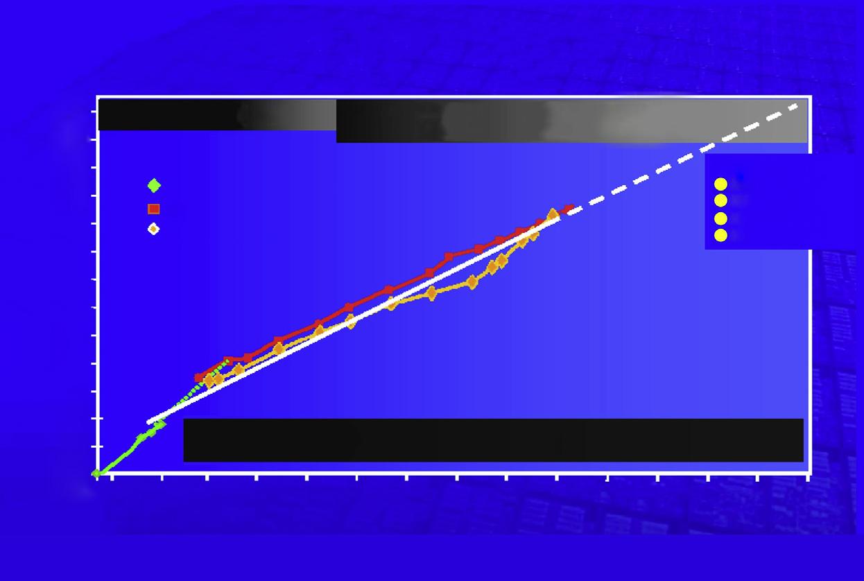
Figure1.1 IllustrationofGordonMoore’slawforSi-CMOS-basedsemiconductormemoryand microprocessor.Pastprogressofmemoryandmicroprocessorisbasedonthislaw.Around 2020,Si-CMOStechnologyisreachingthedead-endandphysicalfabricationlimitsonenergy consumptionandthesizeeffectintheelectric-fieldgating.Thecandidatetogobeyondthe Si-CMOStechnologymaybespintronics,moltronics,quantronics,oratomtronics.
combinedwiththefabricationmethodofSi-CMOStechnologyandspin-degreeof freedom.However,weneedtherealisticsemiconductornanospintronicsmaterials fordevicesthatshouldhavethesuper-highCurietemperature(TC) > 1000Kinorder toavoidthespin fluctuationandtheinstabilityofthemagnetizationcausedbytheweak magneto-crystalanisotropyorshapeanisotropyattheroomtemperature(T ¼ 300K) fortherealizationofrealisticsemiconductornanospintronicsforindustrialapplications. Fortherealizationofsemiconductornanospintronics,weshoulddesignandrealize(1) thesuper-high- TC ferromagneticsemiconductors(TC > 1000K)inwhichwecan controlthespin spininteractionfromferromagnetictoantiferromagnetic(orparamagnetic)bytheelectric-fieldgating,or(2)thesuperparamagneticnanostructurematerials withsuper-highblockingtemperature(TB > 1000K)causedbythemagneto-crystal anisotropyorshapeanisotropyinwhichwecancontrolthemagneticspin spininteractionfromferromagnetictoparamagneticinthenanosuperstructuresofmagnetic semiconductorsbytheelectric-fieldgating(see Fig.1.2).
Todesignandrealizethesenanospintronicsmaterialsbasedonabinitioelectronic structurecalculationandmultiscalesimulationforthedesignandfabricationof self-organizednanosuperstructures,semiconductornanospintronicsmaterials,and alsonanospintronicsdevices,wehavedevelopedtheComputationalNano-Materials Design(CMD®)systemasshownin Fig.1.3
Historically,theprogressoftheindustrialsocietyisbasedonthebasicresearchon thematerials(Materials);wedevelopthedevicesbasedonresearchanddevelopment
1013 1012 1011 1010 109 108 107 106 105 104 103 102 101 100 19601970 Kilo xtor 1965 data (moore) Bipolar PMOS NMOSCMOS Voltage scaling Pwr eff scaling New nonostructures Moore’s law will outlive CMOS 10 μm 1 μm 100 nm 10 nm Memory Microprocessor Beyond CMOS Spintronics Moltronics Quantronic Atomswitch Transistors/die Mega xtor Giga xtor Tera xtor 1980 1990 200020102020 2030
4RareEarthandTransitionMetalDopingofSemiconductorMaterials

Figure1.2 Schematicexplanationofsemiconductornanospintronics [1,3,5].Bycontrollingthe magneticspin spininteractionbytheelectric- fieldgatinginthenanoscalesize,wecan fabricatethesemiconductornanospintronicsdevicesbycontrollingthespincurrent(angular momentum),charge(electric- field),andatomic-masscurrent(kineticenergyorheat)ofthe electrons.
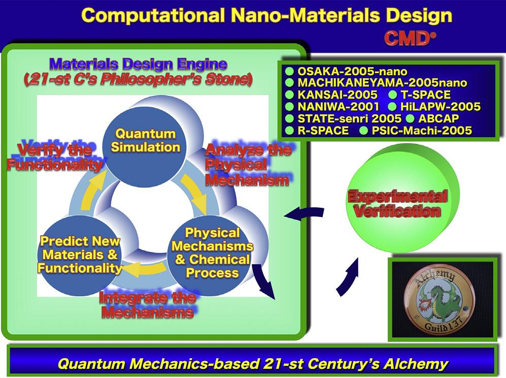
Figure1.3 ComputationalNano-MaterialsDesign(CMD®)System,whichwasdevelopedin OsakaUniversity [1,3,5].Basedontheabinitioelectronicstructurecalculationsandmultiscale simulations,wecananalyzethephysicalmechanismandchemicalfabricationprocess. Thenbasedonthephysicalandchemicalprocessmechanisms,wecanpredictthenew functionalitiesandnewmaterials.Finally,usingthequantumsimulations,wecanverifythe functionalityanddeviceapplicability.CombiningCMD® withtheexperimentalveri fication, wecandesignandrealizethenewfunctionalmaterialsanddevices. Computationalnanomaterialsdesignfornanospintronics5
6RareEarthandTransitionMetalDopingofSemiconductorMaterials
(R&D),wherealargegapcalled “DeathValley” alwaysexistsbetweenthebasic research(Materials)andR&D(Devices)(see Fig.1.4).Then,basedonR&D,we canindustrializethesystemandsoftwarebydevelopingthesystemintegration,where alargegapcalled “Darwin’sSea” alwaysexistsbetweenR&Dandtheindustrialization.In “Darwin’sSea,” astrongcompetitionbetweenthedevelopingcompanyexists andasnaturalselectionalwaysoccurs, fi nallyonlyoneprofitablecompanycansurvive throughinthecompetitivemarket.
Ingeneral,ittakesmorethanhalfacentury,eveninthecaseofsuccessful Si-CMOStechnology,toreachfromthebasicresearchtoindustrializationbythe bottom-updevelopmentthroughthethreehierarchalindustrialstructuresofMaterials, Devices,andSystemandSoftware(see Fig.1.4).Inordertoacceleratethedevelopmentfromthebottomupthroughthehierarchystructures,wehavedevelopedthe CMD® system,wherewestartfromthepredictionanddesignofthelikelyfuture society,andproposethesuitablesystemandsoftwarenecessarytosolvefuture problemsrelatedtoenergy,environment,socialsecurity,andanagingsociety. Then,inordertorealizethesystemandsoftwaretosolveourfutureproblems,we candesignthedevicesbasedontheR&D.Therefore,wecandesignthenewmaterials andfunctionalitiesthatweneedforthedevelopmentofthefunctionaldevicesinR&D. IntheCMD® system,wecanfollowthetop-downmethodologyinordertoshortenthe developmenttimebasedontheCMD® andExperimentalVerifications.
Inthissection, firstofall,wediscusstheferromagneticmechanismindisordered dilutemagneticsemiconductorsandreliableevaluationmethodof TC comparing

Figure1.4 HierarchyofindustrialstructureofMaterials(basicresearch),Devices(R&D),and SystemandSoftware(industrialization) [1,3,5].Oursocietychangesfromanindustrialsociety toaknowledge-basedsociety.Attheinterfacebetweenthedifferenthierarchalstructures,large gapsexist,suchas “DeathValley” and “Darwin’sSea.” Tomakeaseamlessconnection betweenthegaps,weneeddesign-basedmaterialsanddevicefabrication.Here,theoriginality inthematerialsdesignistheoriginofthepro fitabilityinthemarket.
withtheavailableexperimentaldata.Then,wediscusshowtoincreasethe TC by codopinginordertoincreasethesolubilityofmagneticimpuritiesinsemiconductors, superparamagneticphenomenatoincreasetheblockingtemperaturebyspinodalnanodecompositionusingthelowsolubilityofthemagneticimpuritiesinsemiconductors. Wealsodiscusstheshapecontrolofnanomagnetsbycontrollingthespinodalnanodecompositionanddimensionalityofthecrystalgrowth(2Dor3D).Inorderto combinethehighsolubilitybycodoping,high-ef ficiencylightemissionbycodoping, andmagneticinteractionssuchasp-fexchangemechanism,wediscussthenewfunctionalityofrare-earthimpurity-dopedwidebandgapsemiconductors,includingthe circularlypolarizedlightemission.Finally,basedontheseresults,wediscussthe designofd0 ferromagnetismwithout3dtransitionmetal(TM)impuritiesandwithout rare-earthimpuritiesinconventionaloxidessuchasMgO,whereusingthespinodal nanodecompositioncausedbythelowsolubilityofdefectsandimpuritiesbycontrollingthehighblockingtemperatureofsuperparamagnetism.
IntheCMD® System(see Fig.1.3), firstweproposethephysicalmechanismand chemical-reactionmechanismforthefabricationofnewfunctionalmaterialsbasedon theanalysisofthemechanismsbyquantumsimulationsusingthedevelopedapplicationsforthequantumsimulationsandmultiscalesimulations.Second,afterweunderstandthephysicalmechanismandchemicalprocesses,wecandesignandpredictthe newfunctionalmaterialsandprocessmethodsbasedonthequantumsimulationsand multiscalesimulations.Third,thenwecancheckthenewfunctionalitybasedonthe quantumsimulations.Byitineratingthesethreesteps,wecandesignandrealizethe newfunctionalmaterialsbasedonthequantumsimulationsandmultiscalesimulations (see Fig.1.3).
In Section1.2,wediscusstheelectronicstructureofdisordereddilutemagnetic semiconductors,themechanismofferromagneticinteractioncausedbylong-ranged Zener’sp-dexchangeinteraction,andtheshort-rangedZener’sdoubleexchangeinteraction;thecalculationof TC byMonteCarlosimulation(MCS);andthecodoping methodinordertoincreasethesolubilityofmagneticimpuritiestoincreasethepercolationsofshort-rangedmagneticinteractions [2].In Section1.3,wediscussthespinodalnanodecompositionandhighblockingtemperatureofsuperparamagnetismbased onthemultiscalesimulationofthespinodalnanodecompositionbasedontheabinitio calculationandMCSofthecrystalgrowthbycontrollingthecrystalgrowthdimensionality(2Dand3D)inthethermalnonequilibriumcrystalgrowthconditionand dynamicallycreatednewphasessuchas Dairiseki phase(quantumdot)and Konbu phase(nanowire),where TB becomesdominantshowinghysteresiscausedbythelarge magneto-crystalanisotropyandshapeanisotropyinthesuperparamagnetism [6].In Section1.4,wediscusstheelectronicstructureofrare-earthimpuritiesinGaN,computationaldesignofmaterialsforhigh-efficiencylightemission,high-densitydopingof rare-earthimpuritiestorealizethemagnetism,andcircular-polarizedlightemitting diodes(LEDs)basedonabinitioelectronicstructurecalculations.Finally,in Section1.5,wediscusstheelectronicstructureofMgO-basedhigh-TC nanospintronics materialswithd0 ferromagnetism,includingtheelectronicstructure,thed0 ferromagnetismwithoutmagneticTMimpuritieswithveryhigh TB in Konbu and Dairiseki phasescausedbythe2Dand3Dspinodalnanodecomposition. Computationalnanomaterialsdesignfornanospintronics7
8RareEarthandTransitionMetalDopingofSemiconductorMaterials
1.2Disordereddilutemagneticsemiconductors
Thediscoveryofthecarrier-inducedferromagnetismindilutemagneticsemiconductors(DMSs)suchas(Ga,Mn)Asand(In,Mn)Aswasfollowedbyvastseriesofexperimentalandtheoreticalinvestigationsconcerningthefundamentalmechanismofthe ferromagnetismanditsapplicationtothesemiconductorspintronics [7 14].Sofar, ontheferromagnetisminDMS,twoimportantmechanismsareproposedtheoretically. Oneisthep-dexchangemechanism [15,16] andtheotheristhedoubleexchange mechanism [17].Owingtotherecentaccuratetransportmeasurementsanddetailed spectroscopicanalysis,discussiononthedominantmechanismhasbeenreconsidered carefully [18 20].However,thereseemsaconsensusthatthetwomechanismsplay themostimportantroletodescribethemagnetismofDMS.Therefore,inthissection, fi rstwegiveabriefdiscussiononthep-dandthedoubleexchangemechanismsbased onthe first-principlescalculations,andthendescribehowaccuratelywecanpredict TC ofDMSfrom firstprinciples [12].Finally,threestrategiestorealizeroom-temperature ferromagnetismareproposed.
1.2.1p-dexchangeanddoubleexchangemechanisms
MostoftheDMSsystemsaresynthesizedbydopingmagneticimpurities(usually3d TMssuchasMnandCr),incompoundsemiconductorssuchasGaAs,InAs,and ZnTe.Sincethevalencebandofthehostsemiconductorisconstructedfromp-states ofanion,thekeyfactorindeterminingtheelectronicstructureandmagneticstateis therelativepositionbetweend-statesoftheTMionandp-statesoftheanion [12,21].
WhenTMimpuritiesareintroducedinthehostsemiconductors,d-statesofTM hybridizewithp-statesofhostanion.Ifthed-statesofTMarehigherinenergythan p-statesofanion,normallyTMd-statesappearinthebandgapandformimpurity bands.Whentheinducedimpuritybandsarepartiallyoccupied,thebandenergyof thesystemisloweredduetothebroadeningoftheimpuritybands.Sincetheband broadeningeffectivelyoccursintheferromagneticcon fi gurationofmagnetic momentsofTMimpuritiescomparedtoantiferromagneticconfi guration,theferromagneticstateisstabilized.Thiss ituationisschematicallyshownin Fig.1.5(a) Thismechanismisca lleddoubleexchange [17] andisimportanttypicallyinwide bandgapsemiconductor-basedDMSsuchas(Ga,Mn)Nand(Ga,Cr)N,Cr-doped DMS(Zn,Cr)Te,andsoon.Sinceoverlappingwavefunctionscausebandbroadening,theinteractionrangeofthedoubleexchangeisusuallyshortduetothe exponentialdecayofthewavefunctionoftheimpuritystatesthatareusuallylocated inthemiddleofthebandgap.
Ontheotherhand,whenthed-statesofTMarelowerinenergythanthep-statesof anion,TMd-bandsappearatthelowerpartofthevalencebands.DuetothehybridizationbetweenTMd-bandsandthevalencebands,thevalencebandsareshiftedupin energy.IfthemagneticmomentsofTMimpuritiesalignferromagnetically,the valencebandsshownetspinsplitting.Therefore,holedopinginthissysteminduces magneticpolarizationinthevalencebandsandthesystemgainsmagneticenergy. Sincethisenergygainisnotachievedwhenthedirectionofthemagneticmoments
Computationalnanomaterialsdesignfornanospintronics9
Band-broadening
d States
d States
Valence p-band
d States
Valence p-band p-d mixing p-d mixing
d States
Figure1.5 Schematicpictureofthedensityofstatesof(a)doubleexchangesystemand (b)p-dexchangesystem.
FromBelhadjiB,etal.JPhys:CondensMatter2007;19:436227.
areantiferromagnetic(therefore,nomagneticpolarizationofthevalencebands),the ferromagneticstatebecomesstable.Thissituationisillustratedin Fig.1.5(b).This mechanismiscalledp-dexchange [15,16] andisimportanttypicallyinMn-doped narrowgapDMSsystems.Inthep-dexchangesystems,magneticpolarizationof valencebandsmediatesferromagneticinteraction,therefore,theinteractionrangeis intrinsicallylong.
TheelectronicstructureoftypicalIII-VDMSsystemswascalculatedbyusingthe Korringa-Kohn-Rostokercoherentpotentialapproximation(KKR-CPA)withinthe localdensityapproximation(LDA).Calculateddensityofstates(DOS)of(Ga,Mn) N,(Ga,Mn)P,(Ga,Mn)As,and(Ga,Mn)Sbisshownin Fig.1.6[12].Wecanrecognize transitionfromatypicaldoubleexchangesystem(Ga,Mn)N(Fig.1.6(a) tothep-d exchangesystem(Ga,Mn)Sb(Fig.1.6(d)).(Ga,Mn)P(Fig.1.6(b))and(Ga,Mn)As (Fig.1.6(c))areinbetween [12,21,22].
TypicalTMconcentrationinDMSis10 20%.Inthisconcentrationrange,itis crucialforaccurate TC predictiontotaketheinteractionrangeintoaccount.Thisis easilyunderstoodbytheanalogytothesitepercolationproblem.Forexample, whenthemagneticinteractionisextremelyshortandonlythenearestneighborinteractionisimportant,underthepercolationthresholdtheferromagneticnetworkcannot spreadoverthecrystaltomakethewholesystemferromagnetic.Evenabovethe threshold,iftheconcentrationisnothighenough TC mightbesuppressedvery much.Wecallthisthemagneticpercolationeffect,andthiseffectisnotcorrectly consideredinthe TC calculationbythemean fieldapproximation(MFA),because
(a) (b)
Conduction band
E
E
F
F
10RareEarthandTransitionMetalDopingofSemiconductorMaterials
Figure1.6 CalculatedDOSof(a)(Ga,Mn)N,(b)(Ga,Mn)P,(c)(Ga,Mn)As,and(d)(Ga,Mn) SbbyusingtheKKR-CPA-LDA.TotalDOSandpartialdensityofd-statesatMnsiteare plotted.
FromSatoK,BergqvistL,KudrnovskyJ,DederichsPH,ErikssonO,TurekI,etal.RevMod Phys2010;82:1633.
randomdistributionofTMimpuritiesinthecrystalisaveragedoutintheMFA.Forthe calculationof TC beyondtheMFAwehavetoperformMCS.Theimportanceofthe magneticpercolationeffectdependsontheinteractionrange.Forexample,iftheinteractionrangeisinfi nitelylong,theMFAbecomesaccurate.Asexplained,theinteractionrangedependsonthemechanismthatmediatestheferromagneticinteractions,and themechanismreflectstheelectronicstructureofDMS.Therefore,inordertocalculate TC ofDMSaccuratelywithfullaccountofthechemicaltrend,weneedtocalculate effectiveexchangeinteractionsbetweenTMimpuritiesasafunctionofdistance, andthecalculatedexchangeinteractionsshouldbeusedintheMCS [12,23].This pointisdiscussedinthenextsubsection.
1.2.2Reliablecalculationof TC
TheeffectiveexchangeinteractionsbetweenTMimpuritiescanbecalculatedfrom fi rst-principlesbyusingthemappingontheclassicHeisenbergmodel.Intheclassic Heisenbergmodel,themagneticstateofthesystemisdescribedbytheHamiltonian:
H ¼ X isj Jij ei ! $ ej ! ; [1.1] Up spin Down spin Up spin Down spin Down spin Up spin Down spin Up spin (Ga, Mn)N (a)(b) (c)(d) (Ga, Mn)As (Ga, Mn)Sb (Ga, Mn)P Total Mn-3d Total Mn-3d Total Mn-3d Total Mn-3d 3 2 1 0 1 2 3 2 1 0 1 2 3
Energy relative to the Fermi energy (eV) Total and partial DOS (1/eV/unitcell, atom)
–8–6–4–20246–8–6–4–202468
where ei ! denotestheunitvectoralongthedirectionofmagneticmomentatsite i and J ij istheeffectiveexchange interactionbetweensite i and j. Accordingto theLiechtensteinetal., Jij canbeestimatedbyusingthemultiplescattering theoryas:
where dti ¼ t [ i t Y i (t [ i isatomic t-matrixatsite i forspin-upstate), sij isthescattering pathoperatorconnectingsites i and j, ε istheenergy,and εF istheFermienergy [24]. ThisexpressioncanbeeasilyevaluatedintheframeworkoftheKKR-CPAmethodto describethesubstitutionaldisorder.
Calculated Jij showsaclearchemicaltrendasshownin Fig.1.7[22].In(Ga,Mn)N, theinteractionrangeisquiteshort,refl ectingthedoubleexchangenatureofthe exchangeinteractionsinwidebandgapsemiconductors.In(Ga,Cr)N,thecalculated Jij isalsoveryshortrange.Sincethenearestneighborinteractionisverylarge, TC bytheMFAbecomesveryhighevenforlowconcentration.However,thishigh TC istheartifactoftheMFAandrealisticestimationof TC bytheMCSgivesavery
Figure1.7 CalculatedexchangeinteractionsbetweenMnimpuritiesin(a)(Ga,Mn)N, (b)(Ga,Mn)P,(c)(Ga,Mn)As,and(d)(Ga,Mn)Sbasafunctionofdistance. FromDederichsPH,SatoK,Katayama-YoshidaH.PhaseTransitions2005;78:851. Computationalnanomaterialsdesignfornanospintronics11
Jij ¼ J 1 p Z εF N dti sij dtj sji d ε; [1.2]
14 12 10 8 6 4 2 0 4 3 2 1 0 1% (Ga, Mn)P (Ga, Mn)Sb (Ga, Mn)As (Ga, Mn)N (a)(b) (c)(d) 1% 5% 15% 1% 15% 5% 3% 5% 15% 5% 15% 012345 0.8 0.6 0.4 0.2 0 –0.2 –0.4 012345 1.4 1.2 1 0.8 0.6 0.4 0.2 0 012345 012345 Distance (lattice constant)Distance (lattice constant) Distance (lattice constant) Distance (lattice constant) Exchange interactions (mRy) Exchange interactions (mRy) Exchange interactions (mRy) Exchange interactions (mRy)
lowvalue.Therefore,thedoubleexchangesystemisrealisticashigh-TC DMSonly whenhighconcentrationdopingispossible.
Ontheotherhandin(Ga,Mn)Sband(Ga,Mn)As(Fig.1.7(d)and(c)),the interactionrangeisrelativelylongduetothep-dexchangenatureoftheexchange interactions.Inthep-dexchangesystems,theinteractionsaregenerallyweak comparedtothedoubleexchangesystems;however,duetothelongrangenatureof theinteractionsthep-dexchangehasanadvantageoverthedoubleexchangefor lowconcentrationtorealizetheferromagnetism.Actually,sofarthebestinvestigated DMSsare(Ga,Mn)Asand(In,Mn)As.
(Zn,Cr)Teand(Ga,Mn)Pareinbetweenthedoubleexchangeandthep-d exchange.Asexplainedintheprevioussubsection,therelativeimportanceofthe twomechanismsdependsontherelativelocationofTMd-statescomparedtothe hostvalencebands,thereforerealsystemsaredistributedbetweentwoextremecases, namelythedoubleandthep-dexchange,showingwidevarietyandthecomplexityof realmaterials.
TypicalresultsoftheMCSfor T C of(Ga,Mn)N,(Ga,Mn)P,(Ga,Mn)As, (Ga,Mn)Sb,(Zn,Cr)Te,and(Ga,Cr)Nareshownin Fig.1.8[12,23,25].For (Ga,Mn)P,(Ga,Mn)As,and(Zn,Cr)Te,theMCSresultsreproduceexperimental resultsverywell.Theoverestimationof TC byMFAandRPAisclearlyseeninthe figureforallsystems,butthedegreeoftheoverestimationdependsontheinteraction range.AccordingtotheMCSof TC itiswellunderstoodthathighconcentration dopingofTMimpuritiesisnecessaryforrealizinghigh TC.Basedonthisguideline towardhigh TC,highconcentrationdopinghasbeenattemptedexperimentally forvarioussystems.However,ithasbeenrevealedthathomogeneoushighconcentrationdopingisquitedifficulttorealizeevenwithnonequilibriumcrystalgrowthtechnique [26].Inthenextsubsection,weproposethreestrategiesforovercomingthis difficulty.
1.2.3Towardhigh TC
Accordingtothe first-principlespredictions,generallyhighconcentrationdopingis neededforrising TC,therefore,lowsolubilityofTMimpuritiesinDMSpreventsus fromrealizinghigh TC.ThisistheintrinsicnatureofDMSandinthepreviousexperimentalfabricationofDMSmaterialsthisdif ficultyhasbeenpartlyovercomebyusing nonequilibriumcrystalgrowthtechniques.However,thetheoreticallyrequired concentrationtoreachroom-temperatureferromagnetismistoohightorealizeand weneedanewapproach.Sofar,wehaveproposedsomematerialdesignsalongthe followingthreedirections.
• Codopingmethod
Oneoftheindicationsofthetendencyforphaseseparationappearsinthecalculatedmixing energy.Themixingenergy DE of(Ga,Mn)Asiscalculatedas:
DE ðxÞ¼ E ðGa1 x Mnx AsÞ ð1 xÞE ðGaAsÞ xE ðMnAsÞ; [1.3] 12RareEarthandTransitionMetalDopingofSemiconductorMaterials
0246810121416
0246810121416 Mn concentration (%) Mn concentration (%)
0246810121416
Mn concentration (%)
Cr concentration (%)Cr concentration (%)
Figure1.8 CalculatedCurietemperatureof(a)(Ga,Mn)N,(b)(Ga,Mn)P(c)(Ga,Mn)As, (d)(Ga,Mn)Sb,(e)(Ga,Cr)N,and(f)(Zn,Cr)Te.Curietemperatureiscalculatedasafunction ofTMconcentration.MFA,randomphaseapproximation(RPA),andMCSwereusedforthe calculations.Thenumbersarereferencesfortheexperimentalresults.
FromSatoK,FukushimaT,Katayama-YoshidaH.JPhys:CondensMatter2007;19:365212.
where x istheconcentrationofMnand E( x )istheenergyofcompound X,respectively. Byde fi nition,positive D E indicatesthat(Ga,Mn)AsfavorsphaseseparationtoGaAs andMnAs.Re fl ectingtheexperimentallowsolubilityofMninGaAs,themixingenergy of(Ga,Mn)Asiscalculatedtobepositive.Positivemixingenergyisalsocalculatedfor
800 700 600 500 400 300 200 100 0 800 700 600 500 400 300 200 100 0 0510152005101520 350 300 250 200 150 100 50 0 350 300 250 200 150 100 50 0 0246810121416 350 300 250 200 150 100 50 0 350 300 250 200 150 100 50 0 1 2 1 3 MFA 7 RPA MFA MCS 6 Experiment (Ga, Mn)P RPA MCS (Ga, Mn)N (a)(b) (c)(d) (e)(f)
Curie
Curie
(K)
Curie temperature (K) Curie temperature (K) Curie temperature (K)
temperature (K) Curie temperature (K)
temperature
Mn concentration (%) (Ga, Mn)Sb MFA RPA MCS 12 (Zn,
MFA RPA 15, 16 Experiment MCS MCS 14 Experiment 13 RPA MFA (Ga, Mn)As Experiment 8 8 8 9 MCS RPA MFA Experiment 4 5 10 11 9 9 (Ga, Cr)N Experiment
Cr)Te
Computationalnanomaterialsdesignfornanospintronics13
14RareEarthandTransitionMetalDopingofSemiconductorMaterials
theotherDMSsystems,suchas(Ga,Mn)N,(Ga,Cr)N,(Zn,Cr)Te,andsoon, andcorrespondsreasonablytotheexperimentalobservationofphaseseparationin theseDMS.
Inthecodopingmethod,inadditiontoTMimpurities,carrierdopantsareintroduced simultaneously.TheadditionalcarrierdopantsshouldbechosensothattheycompensatecarriersoriginatingfromTMimpurities.SincetheTMimpuritynormallybehavesasan acceptor,inthecodopingforDMSweshouldchoosedonorimpurities.Duetotheintroductionofcodopants,themixingenergyofTMimpuritiesisloweredandphaseseparationis suppressed,leadingtohighsolubility [27].Thisisanadvantageofthecodoping,butit hasadisadvantagetoo.Becauseofthecompensationofholecarriers,theferromagnetism isweakenedduetothecodoping.Therefore,afterthecrystalgrowthbyusingthecodoping method,thecodopantsshouldberemovedfromthecrystaltorecovertheferromagnetism. Fromthispointofview,mobileinterstitialdonorimpuritiesareproposedasgoodcodopants forDMS.IthasbeenshownthatLiinterstitialworksideallyasthecodopantfor(Ga,Mn)As [28,29].Asanotherpossibilityofcodoping,rare-earthimpurityandN-vacancycodopingin GaNwillbeproposedin Section1.4.
• Superparamagneticblockingphenomena Sofar,wehavefocusedonthehomogeneousDMSsystems.ThehomogeneousDMSmight beeasytohandlewhenweconsiderthefabricationofspintronicsdeviceswithhighreproducibility.IfweareonlyinterestedinferromagneticbehaviorofDMS,wecanmakeuseof inhomogeneous(namelyphaseseparated)DMS.TheinhomogeneousDMScanbeconsideredahybridmaterial,whereforexamplein(Ga,Mn)Ascase,nanomagnetsofMnAs(or (Ga,Mn)AswithhighconcentrationofMn)areembeddedinthehostsemiconductor GaAs.Thesenanomagnetsareexpectedtohavehigh TC,butduetotheabsenceofmagnetic exchangeinteractionbetweennanomagnetsthesystembecomessuperparamagnetic.Ifthe sizeofthenanomagnetsissmallenoughtobesinglemagneticdomainandthemagnetic anisotropyisimportant,thedirectionofmagnetizationofthenanomagnetis fixedalong themagneticeasyaxis.Sincethemagnetizationreversalisblockedbelowtheblockingtemperature(TB),thesystemlookslikeferromagnetsfor T < TB.Sincewecancontrolthesizeof thenanomagnetsbytuningcrystalgrowthcondition,materialsdesignforhigh-TB inhomogeneousDMSispossible [30].Anexampleofmaterialsdesignalongthisideawillbe describedin Section1.3.
• Searchfornewmaterials
ForgettingabouttheadvantageofusualIII-Vsemiconductorsthathavecompatibility withthepresentelectronicsandextendinghostmaterialstootherthanIII-Vsemiconductors,wecanchooseexoticsemiconductorsashostsemiconductorsfornewDMS.For example,IV-VIsemiconductorsuchasGeTeisknowntoshowhighsolubilityofTM impuritiesandmaterialsdesignofGeTe-basedDMSwasproposed [31,32].Thetheoreticalpredictionwaspartlysupportedbyexperimentalresults.Wecanchooseevenoxides ashostmaterials.Duetothestronglycorrelatednatureofoxides,thereisapossibilityto realizeferromagnetismwithoutanyTMimpurities.Thisiscalledd 0-magnetism [33 36] andisdiscussedindetailin Section1.5 togetherwithself-organizationofnanostructures inoxides.
Inthissection,wehavediscussedtheoriginoftheferromagnetismand first-principles methodforcalculating TC ofDMS.ItisemphasizedthatthemagneticpercolationisimportanttounderstandanddesignthemagneticpropertiesofDMS.Basedonthisknowledge,we havediscussedthreepossibledirectionstowardhigh-TC DMSmaterials.Someofthemwill bediscussedfurtherinthenextsections.
1.3Spinodalnanodecompositionandhigh blockingtemperature
Asdiscussedin Section1.2.3,theinhomogeneityinDMSsystemshasattractedalot ofattention,becausethisfeaturecouldopenthewaytonewandnovelspintronic devicesbyutilizing TB.Suchamovementstartedwiththeinconsistencybetween thetheoryandexperiment;thatis,intheexperiments [26,37,38],roomtemperatureferromagnetismwasobservedforlowconcentrationofthemagneticimpurities,whereasthetheorypredictedverylow TC forlowconcentrationofthemagneticimpuritiesduetothemissingmagneticpercolation [12].In2006,Satoand Katayama-Yoshida [39] proposedthatspinodalnanodecomposition(spinodal decompositioninnanoscalesize)isanimportantrolefortheinhomogeneityin DMS,basedonabinitiocalculations.Sincetheirwork,manypeoplehavebeen interestedintheinhomogeneityofthemagneticimpuritiesinDMS,andthenthespinodalnanodecompositionhasbeenactuallyobservedintheexperiments [40,41],as shownin Fig.1.9.Inthissection,wewillpresentthetheoreticalinvestigationsofthe inhomogeneityinDMSsystemsbyabinitiocalculations,andalsodemonstratethe simulationofthe2D(Konbu-phase)and3D(Dairiseki phase)spinodalnanodecompositionsbytheMonteCarlomethod.
1.3.1Mixingenergy
WebeginbydiscussingmixingenergyinDMSsystems. Fig.1.10 showsthemixing energiesof(a)(Ga,Mn)N,(b)(Ga,Cr)N,(c)(Ga,Mn)As,and(d)(Zn,Cr)Tebythe redlinesasafunctionoftheTMimpurityconcentration [12,42].AlltheseDMSsystemshaveconvexconcentrationdependenciesofthemixingenergywiththepositive values,leadingtothephaseseparation;thesefoursystemshavethemiscibilitygaps. Inthecalculationsof Fig.1.10,thecrystalstructureisassumedtobezincblende structure.Therefore,theseDMSsystemsundergothephaseseparationcoherently withkeepingthezincblendestructure;forexample,forthecaseof(Ga,Mn)N, thezincblendeGaNandMnNaregeneratedinthecrystal.Inparticular,(Ga,Mn) Nand(Ga,Cr)Nwiththeirwidebandgapshavethelargermixingenergies,compared tothecasesof(Ga,Mn)Asand(Zn,Cr)Te.Inthissense,itisconsideredthatthefabricationofhomogeneousnitrideDMSsareverydifficultbyexperiment.Wenotethat sincethecalculationsin Fig.1.10 areperformedbytheKKR-CPAmethod,thestructuraloptimization,whichcausesthereductionofthemixingenergy,isnottakeninto account.Wecanseetheeffectofstructuraloptimizationformixingenergybythe supercellcalculationandclusterexpansionmethodin [43].In Fig.1.10,themixing energiescalculatedbythecodopingmethodarealsoshown.Byintroducingadditional codopants,suchasO,N,andIatoms,intoDMS,wecandrasticallyreducethemixing energy,sothatthesolubilityoftheTMimpuritiesincreases [28,29].Thisisdueto theenergygainbytheself-compensationbetweentheTMimpurities(acceptor)and codopant(donor).ThepreviousdiscussionfocusedonthephasestabilityofDMS
Computationalnanomaterialsdesignfornanospintronics15
16RareEarthandTransitionMetalDopingofSemiconductorMaterials


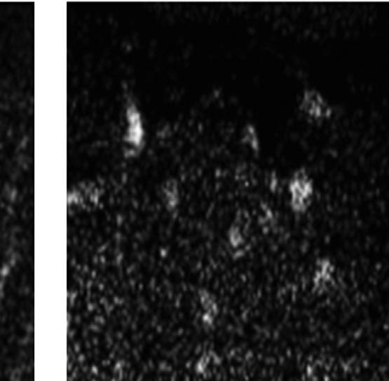
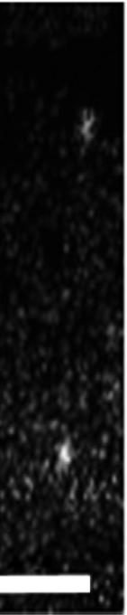
Figure1.9 (a)Colormapofthehighestdoped(Ga,Mn)Nsample(Mn ¼ 11%). Red, blue,and green correspondtotheMn-Ka,Ga-Ka fluorescenceline,andinelastic(Compton)scattering signal,respectively.Ga(in black)andMn(in red)profilesalongthewhitescanlineareshown inthelowerpart. (FromMartínez-CriadoG,SomogyiA,RamosS,CampoJ,TucoulouR, SalomeM,etal.ApplPhysLett2005;86:131927.) (b)Energy-filteredelectronmicrographs showingCrdistributionfor4%Cr-dopedAlNgrownatdifferentsubstratetemperatures: (i)700 C;(ii)800 C. (FromGuL,WuSY,LiuHX,SinghRK,NewmanN,SmithDJ.JMagn MagnMater2005;290 291:1395.)
(Ga,Mn)N (Al,Cr)N
Mn-K
GaescapepeakMinpile-up 67891011 Energy(keV) Mn
Scattering 40 nm 30 nm Low(Mn) Mn-K Ga-K Ga-K α α Mn-Kβ β GaescapepeakMinpile-up 67891011 Energy(keV) Fluorescence Ga-Kα Mn-Kα 0.10 0.05 0.00 1.0 0.9 0.8 01020 X(μm) 304050 Profiles (i) (a) (b) (ii) 25 μ m
High(Mn)Ga-Kα
α Mn-Kβ Ga-Kβ
Ga

Figure1.10 Calculatedmixingenergiesof(a)MninGaN,(b)CrinGaN,(c)MninGaAs,and (d)CrinZnTe.
FromSatoK,BergqvistL,KudrnovskyJ,DederichsPH,ErikssonO,TurekI,etal.Rev ModPhys2010;82:1633;SatoK,FukushimaT,Katayama-YoshidaH.JpnJApplPhys2007; 46:L1120. Computationalnanomaterialsdesignfornanospintronics17
systemsatzerotemperature.For finitetemperature,weneedtocalculatethemixing freeenergy: FM ðcÞ¼ EM ðcÞ TS;
where T istemperatureand S ismixingentropy.Fromthebehaviorofthemixingfree energy,thephasediagramsofthespinodaldecompositionandbinodaldecompositions canbeeasilydescribed.
1.3.2Chemicalpairinteraction
Asinthepreviousdiscussion,thegeneralDMSsystemsundergothespinodalnanodecomposition,sothatthedistributionofthemagneticimpuritiesinDMSisnolonger homogeneous.Inordertocloselyinvestigatetheconfigurationofthemagnetic impuritiesunderthespinodalnanodecompositionandhowtheinhomogeneityofthe
[1.4]
2525 2020 10 10 15 15 5 05 00.20.40.60.810 00.20.40.60.8100.20.40.60.81 00.20.40.60.81 –5 Mixing energy (mRy) Mixing energy (mRy) Mixing energy (mRy) Mixing energy (mRy) MnconcentrationCrconcentration MnconcentrationCrconcentration Undoped UndopedUndoped Undoped O:5% O:5% O:5% O:10% O:10% O:10% O:15% O:15% O:15% GaMnNGaCrN 3 4 2 1 0 –1 GaMnAsZnCrTe I:15% I:10% I:5% 10% 15% 10N:5% 8 6 4 2 0 –2 –4 (a)(b) (c)(d)
18RareEarthandTransitionMetalDopingofSemiconductorMaterials
magneticimpuritiesaffectsthemagnetisminDMS,wecalculatethechemicalpair interaction.ForabinaryalloyA1 cBc,thechemicalpairinteractionbetweensites i and j, Vij,isde finedby:
where V AB ij ispotentialenergywhentheAandBatomsoccupythe i and j sites, respectively.Asunderstoodfromthedefinition,thenegative Vij meansattractive interaction,whereasthepositiveoneleadstorepulsiveinteraction.Ducastelleand Gautier [44] proposedaprescriptiontocalculatetheeffectivepairinteraction,nowcalled generalizedperturbationmethod(GPM).ThedevelopmentofGPMforKKR-CPA formalismwasdonebyTurchi [45].InGPM,thechemicalpairinteractioncanbe calculatedby
Here, tA(B) isthesinglesite t-matrixoftheatomA(B)and T ij isthescattering pathoperator. Fig.1.11 showsthechemicalpairinteractionin(a)(Ga,Mn)N, (b)(Ga,Cr)N,(c)(Ga,Mn)As,and(d)(Zn,Cr)Teasafunctionofthedistance betweenthetwomagneticimpurities.Asshownin Fig.1.11 ,mostchemicalpair interactionsofthesesystemshavethenegativevalues,leadingtoattractiveinteraction,andthe fi rstnearestneighborin teractionsareconsiderablystrongcompared totheotherpairs.Therefore,(Ga,Mn)N,(Ga,Cr)N,(Ga,Mn)As,and(Zn,Cr) Teundergophaseseparationduetotheattr activepairinteractions;thespinodal nanodecompositioncanoccurduringthe crystalgrowth.Suchtendencyofthe chemicalpairinteractionsisconsistent withthecalculatedconvexpositivemixing energyin Fig.1.10 .
1.3.3Simulationofthespinodalnanodecomposition: Dairiseki phaseversus Konbu phase
BasedonthechemicalpairinteractioncalculatedbytheGPM,wecansimulatethe spinodalnanodecompositioninDMSbyusingtheMonteCarlomethod.Thespinodal nanodecompositionisakindofphaseseparationinalloys.Forcasesofphaseseparationsinalloys,theordinaryIsingmodel,wheretheorderparameterisnotconserved,is notappropriate.Therefore,acorrectmodeltodescribephaseseparationsofalloysis theconservedorderparameterIsingmodel:
H ¼ 1 2 X isj Vij si $ sj ;
where Vij isthechemicalpairinteraction. si istheoccupationnumberofan impurityatomatsite i;thatis, s i ¼ 1ifsite i isoccupiedbyaTMimpurity,
AA
þ V BB ij
V AB ij ;
Vij ¼ V
ij
2
[1.5]
Vij ¼ 1 p Z ImTr L DT ij DT ji d ε; D ¼ t 1 A ðεÞ t 1 B ðεÞ: [1.6]
[1.7]
Computationalnanomaterialsdesignfornanospintronics19

Figure1.11 Chemicalpairinteractionsbetween(a)MninGaN,(b)CrinGaN,(c)MninGaAs, and(d)CrinZnTeasfunctionofdistancenormalizedtothelatticeconstant.Negative interactionsindicatethatthepairinteractionsareattractive.
FromSatoK,BergqvistL,KudrnovskyJ,DederichsPH,ErikssonO,TurekI,etal.RevMod Phys2010;82:1633;FukushimaT,SatoK,Katayama-YoshidaH,DederichsPH.JpnJAppl Phys2006;45:L416.
whereas si ¼ 0ifsite i isoccupiedbyahostatom.Here,weapplyKawasaki algorithm [47] fortheconservedorderparameterIsingmodel.
1.3.3.1 Dairiseki phase
First,thesimulationsofspinodalnanodecompositionfor3Dcrystalgrowthareconsidered.Inthiscase,alargeface-centeredcubic(FCC)supercellisprepared,andthenthe TMimpuritiesinDMSarerandomlydistributedasaninitialconfiguration.Starting fromtherandomdistributionoftheimpurities,wechooseoneimpuritysiteandtry tomovetheimpuritytoasitethatischosenfromtheunoccupiednearestneighborsites byobeyingtheMonteCarlocriterion.Thetrialsitecanbeanyoneofthenearest neighborsites,(ie,oneofthe12sitesinFCCcase).
Fig.1.12(a)and(c) showthesimulationresultsofthe3Dspinodalnanodecompositionfor(Zn,Cr)Teand(Ga,Mn)N, respectively.These figuresarethesnapshotsofTMimpuritydistributionafter100 MonteCarlostepsperthemagneticsite.OnlyCrandMnimpuritiesareindicated bytheredpointsandthenearestneighborbondsarecombinedbythewhitebars. Theimpurityconcentrationis fixedto5%forallcasesandwetake17 17 17conventionalFCCcellsasasimulationbox.Thesimulationsareperformedatscaledtemperatureof kBT/V01 ¼ 0.5foreachcase.Thiscorrespondsto916and2164Kfor
20RareEarthandTransitionMetalDopingofSemiconductorMaterials

Figure1.12 Simulatedspinodalnanodecompositionphasesinthebulk(a)(Zn,Cr)Teand (c)(Ga,Mn)N,andin(b)(Zn,Cr)Teand(d)(Ga,Mn)Nunderthelayer-by-layergrowth condition.Inthe figures,onlymagneticsitesareindicatedbythe redpoints.Theconcentration ofmagneticimpuritiesis5%foreachcase.
FromSatoK,BergqvistL,KudrnovskyJ,DederichsPH,ErikssonO,TurekI,etal.RevMod Phys2010;82:1633;FukushimaT,SatoK,Katayama-YoshidaH,DederichsPH.JpnJAppl Phys2006;45:L416.
(Zn,Cr)Teand(Ga,Mn)N,respectively.Thesesystemsarequenchedfrom T ¼ N to T ¼ 0:5kB jV01 j atthe0MonteCarlostep.Asshownin Fig.1.12(a)and(c),the magneticimpuritiesformmoreisolatedclusterwithincreasingtheMonteCarlosteps, comparedtotheinitialrandomconfiguration,sothatthesystemsbecomesuperparamagnetic.Wecallsuchspinodalphase “three-dimensional Dairiseki phase,” where Dairiseki meansthemarbleinJapanese.Actually,thethree-dimensional Dairiseki phasewasexperimentallyobservedin(Ga,Mn)N,(Ga,Cr)N,(Al,Cr)N,and (Zn,Cr)Te [26,41,48,49].Itiseasilyspeculatedthatthesecomplicatedconfi gurations ofthemagneticimpuritiesstronglyaffectthemagnetisminDMSsystems.The TC valuesof(a)(Ga,Mn)N,(b)(Ga,Cr)N,(c)(Ga,Mn)As,and(d)(Zn,Cr)Tewith the Dairiseki phasecalculatedbyRPAarepresentedin Fig.1.13.Thehorizontal axisistheMonteCarlostepcorrespondingtotheannealingtimeinacrystalgrowth experiment.TheRPAmethodcanexactlytakethemagneticpercolationeffectinto consideration,andprovidetherealisticestimationof TC.Sincethecalculatedresults dependontheinitialconfi gurationofthemagneticimpuritiesinthesimulationbox, wesimulatethe30differentspinodalnanodecompositionphasestotakeconfiguration
(a)(b) (c)(d)
Computationalnanomaterialsdesignfornanospintronics21

LDA+U, LDA+U, LDA+U, U =0.3Ry, J =0.06Ry U =0.3Ry, J =0.06Ry U =0.18Ry, J =0.074Ry
Figure1.13 T C RPA of(a)(Ga,Mn)N,(b)(Ga,Cr)N,(c)(Ga,Mn)As,and(d)(Zn,Cr)Teasa functionofthenumberofMonteCarlostepsperimpurity.AsincreasingtheMonteCarlo steps,thephaseseparationdevelops.Forhigherconcentrations, TC increasesduetothe increasedpercolationpathbyclustering.Ontheotherhand,forlowerconcentrations, TC decreasesandthesystembecomessuperparamagnetic.
FromSatoK,BergqvistL,KudrnovskyJ,DederichsPH,ErikssonO,TurekI,etal.Rev ModPhys2010;82:1633;SatoK,Katayama-YoshidaH,DederichsPH.JpnJApplPhys 2005;44:L948.
average.Asshownin Fig.1.13,inthecaseofthelowmagneticimpurityconcentrations,the TC valuesdecreasewiththeMonteCarlostep.Suchatendencycanbe understoodfromthefactthattheferromagneticinteractionsworkonlyinthesmall clusters,howevercannotspreadovertheentirecrystal(ie,thesuperparamagnetism isstableinthecaseofthelowTMimpurityconcentration).Ontheotherhand,the calculated TC valuesincreasewiththeMonteCarlostepinthehighconcentration regionabovethepercolationthreshold.Thisisbecausethemagneticimpuritiescan establishthemagneticpercolatingpathswithformingthelargeclusters.Therefore, thestrongferromagneticinteractions,originatingfromthe fi rstnearestneighboratoms, cancontributethehigh TC.
1.3.3.2 Konbu phase
Next,thenonequilibriumlayer-by-layercrystalgrowthsimulationswiththe2Dspinodalnanodecompositionareintroduced [46].Inthissimulation,theatomicdiffusionis restrictedonlyonthesurface,andonlythenearestneighborsitesonthesamesurface canbecandidatesforatrialsiteinthelayer-by-layersimulation(oneofthefoursitesin
600 500 400 300 200 100 0 5% 5% 5% 15% 15% 15% Cr:10% Cr:15% Cr:20% Cr:5% 20% 20% 20% 30% 30% 30% Curie temperature (K) 600 500 400 300 200 100 0 Curie temperature (K) 600 500 400 400 300 300 200 200 100 100 0 0 Curie temperature (K) Curie temperature (K) (Ga,Mn)N (Ga,Mn)As
(Ga,Cr)N (Zn,Cr)Te
MonteCarlostepMonteCarlostep (a)(b) (c)(d)
020406080100020406080100