
5 minute read
Global leaders in PCBs AT&S


GLOBAL LEADERS IN PCBs
Former Austrian state-owned printed circuit board maker AT&S is currently Europe’s largest circuit board manufacturer and one of the market leaders in high-end printed circuit board technology. Industry Europe looks at the reasons behind its success.


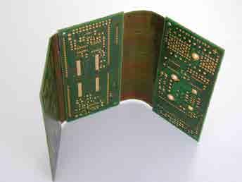
Austrian circuit board maker AT&S (Austria Technology & System Engineering Corporation) is the largest and most technologically advanced producer of printed circuit boards in Europe. Its printed circuit boards (PCBs) are used as electromechanical linking elements, predominantly in the telecommunications sector (for example, mobile phones), as well as in the automobile industry and industrial and medical technology.
Its thin, highly complex printed circuit boards make it a key supplier to leading players across the telecommunications industry. The product portfolio ranges from single and double-side to multilayer printed circuit boards at the frontier of technology.
Post-privatisation success
AT&S was formed from three state-owned companies that unified as one company under a single name, and privatised through a management buy-out in 1994. It pursued a strategy of focusing on the mobile phones business throughout the 1990s and into the early years of the new millennium, but the subsequent downturn in the industry provided the incentive for spreading risk across a broader product portfolio.
“During the 90s AT&S was dedicated to the mobile phones industry and enjoyed the benefits of tracking a strong market. This growth was so dynamic that we decided


to become one of the main suppliers to just two of the largest players, Nokia and Siemens. Our strong partnership with these companies carried us when the PCB industry suffered hard times at the turn of the century,” explained a company representative.
In 2008, AT&S was listed on the Vienna stock exchange, followed in 2009 by the restructuring and reorientation of its Leoben plant towards a high-value industrial business. It was in this year that its Shanghai business also became focused on the high-end mobile devices segment. In 2010, the group headquarters were relocated from Vienna to Leoben-Hinterberg. The year 2011 saw the acquisition of land and the start of the construction of its plant in Chongqing, China. Application areas
Key areas of application include PCBs for measurement technology and large industrial machines. Demand for PCBs in the automotive industry is driven by the increasing number of electronics installed in vehicles. The automotive industry accounts for 12 to 14 per cent of turnover. AT&S aims to focus on profitable niches where the PCB satisfies special requirements, like ‘zero defects’ demanded for ABS, as well as internal lighting or electronic windows.
Within AT&S, industrial is the fastest growing segment and has been for the last two years. Industry customers want smaller volumes, but greater engineering support. It is essential to be close to customers.
For this reason most of its industrial customers are European, while it has telecommunications and automotive customers worldwide. The automotive market is one of the largest markets in Europe but it is very mature and slow moving. Demand for PCBs from the automotive industry reflects this. It takes about two years of preliminary work to qualify for an order and then the product runs for about four or five years until the model is upgraded or replaced.
A new technology segment
Recently, AT&S made the first moves towards entering a new technology segment. It will be expanding its portfolio with the production of integrated circuit (IC) substrates and entering into a further high-tech business segment. IC-substrates serve as a connection between semiconductors and printed circuit boards.


The company’s management decided to make this move in recognition of the trend that is bringing requirements for semiconductors and printed circuit boards ever closer together, and converging production technologies. The production of IC-substrates will be in China. AT&S will build up the necessary know-how with support from a leading semiconductor manufacturer and will enter the market in close cooperation with the same. Investment in this new area of production is expected to total around €350 million, excluding start-up costs.
Focused production
Production is organised across four sites in Austria – Leoben-Hinterberg, Fohnsdsorf, Fehring and Klagenfurt – and at Nanjangud, India and Shanghai, China. AT&S acquired the plant at Nanjangud in 1999 after the parent company Indal decided to concentrate on its core business and sold off the site.
At Leoben, the largest plant in Austria, and at Shanghai, production is focused exclusively on PCBs for mobile phones. At Fehring, Fohnsdsorf and Nanjangud, it is split between PCBs for the automotive industry and industrial applications. Klagenfurt concentrates exclusively on manufacturing PCBs for automotive applications.
Leveraged research
R&D plays a crucial role in maintaining the company’s position as one of the leading players in the PCB market. Direct investment in R&D accounts for about 2.5 per cent of turnover. In addition, it benefits from an R&D network set up with suppliers, customers and research bodies, as the company representative explained: “R&D is very important, and so we have divided this into industrial research and scientific research. As one of the leaders in PCB technology, we need to invest substantially in R&D in order to keep our position.
“You have to innovate, and there are small things like surface treatments where you can bring new technologies to the market and have a unique selling position. Our customers in the mobile phone business will not deal with a supplier if other suppliers do not have the same technology. This is because they cannot run the risk of total reliance on a single source. While such developments confer an advantage for a short period of time, very important innovations are patented.” n


