9 minute read
TEST Enabling High Volume Data Communication – Solving the New Challenges in PIC Wafer Testing
from MEPTEC Report Spring 2023
by MEPTEC
Tobias Gnausch Product Manager UFO ProbeTM Technology JENOPTIK Optical Systems GmbH
Abstract
The volume of data in the digital world has been steadily increasing in recent years. [1] Besides data centers, high-performance computing (HPC) and applications that use artificial intelligence (AI) are currently the drivers, where unbelievable quantities of data must be received, converted, and transmitted in the shortest possible time. The prerequisites for this are fast data transmission and low energy consumption. Photonics plays a key role here as optical transceivers are the essential components in optical communication, along with fiber optics as the transmission medium. The core of such transceivers is the photonic integrated circuit (PIC), the chip of the future. They are manufactured in the same way as classical electrical chips (IC). The testing at waferlevel is a challenge, since not only electrical but also optical components are integrated on the chip. [2] Jenoptik presents with its UFO ProbeTM Card[3] a test-solution that enables a parallel testing by using existing test-infrastructure.
Introduction
Wherever large data streams are handled and large computing power is required, properties such as bandwidth, total energy consumption, and efficiency as well as latency during transmission are decisive factors. Photonic integrated circuits (PICs) offer several advantages in this regard. Unlike purely electrically integrated circuits (ICs), PICs additionally incorporate optical functionalities. Since light can be modulated very quickly while different wavelengths and polarization states do not influence each other, a large data bandwidth is achievable. Data can also be transmitted with low loss over very long distances by means of light. PICs are designed to be very energyefficient, as the integration of electrical and optical components on a single chip makes the electrical transmission channels shorter, which also improves the latency times. PICs are also manufactured on wafers and based on the lithography processes commonly used in the IC semiconductor industry. Those processes are well known and have been tested for decades.
Hence, PICs can benefit from the existing infrastructure of the IC microchip production and the experience gained there. The difference is the addition of optical waveguides and new types of optical active components, which have different require- ments for the manufacturing processes. It is therefore important to precisely control and monitor the manufacturing process and to check the functionality of each individual PIC on the wafer.
I. PIC Wafer-Level Test
Usually the microchips, also often referred to as dies, are checked for functional defects when all manufacturing steps are finished and the dies are not yet separated, but still on the wafer. This is called Wafer-Level Test, Wafer Sort, or Wafer Final Test. The testing is carried out using wafer probers and automatic test equipment (so-called “testers”). Here, the electrical contacting of the chips on the wafer is done by means of probe cards, where microscopic needles establish the electrical contact to the interfaces on the die (bond pads or solder bumps). With this technology, it is even possible to contact and test all chips on a 300 mm wafer simultaneously with one probe card. These probe cards then have several tens to hundreds of thousands of needles and are typical used for memory devices. [4]
In photonic integrated circuits optical interfaces are implemented in addition to the electrical contacts. These can be grating couplers arranged on the chip’s surface analogue to electrical contact pads or edge couplers where the actual waveguide ends at the edge of the respective chip and there light is coupled into the device. This makes aligning the wafer to the probe card and thus testing a challenge: electrical contacts are relatively large, ranging in sizes up to 150 µm in diameter or sometimes even larger. Thus, commercially available wafer probers, which were primarily developed for electrical testing, possess a positioning tolerance between 1.5 and 4 µm in the lateral direction. However, to ensure stable optical coupling, the positioning of the wafer to the illumination unit (e.g., optical fibers) of the test system must be well below the mode field diameter (MFD) of the optical interfaces of the chips. Typical values for the MFD of grating couplers are 10 µm and for edge couplers in the range of 1-2 µm. Accordingly, a positioning accuracy in the sub-micron range is necessary here. Previous commercially available wafer-level test systems for PICs solve this problem by active alignment. [5,6] In this process, the optical fibers or fiber arrays are aligned to the corresponding interfaces on the wafer via positioning systems (e.g., piezo actuators). At the same time, the intensity of the light coupled into the chip is measured. Via feedback loop this value is used to optimize the alignment, which makes it possible to react very flexibly to different layouts. At the same time, a very low coupling loss can be achieved.
However, the fibers must be realigned for each chip. Although this process has been optimized in the recent time, it can still take one to two seconds, depending on the chip and system. [6] For series production in large quantities, this results in a time and cost impact that should not be underestimated. Furthermore, special equipment such as servo motors (hexapods) and special control software needs to be integrated.
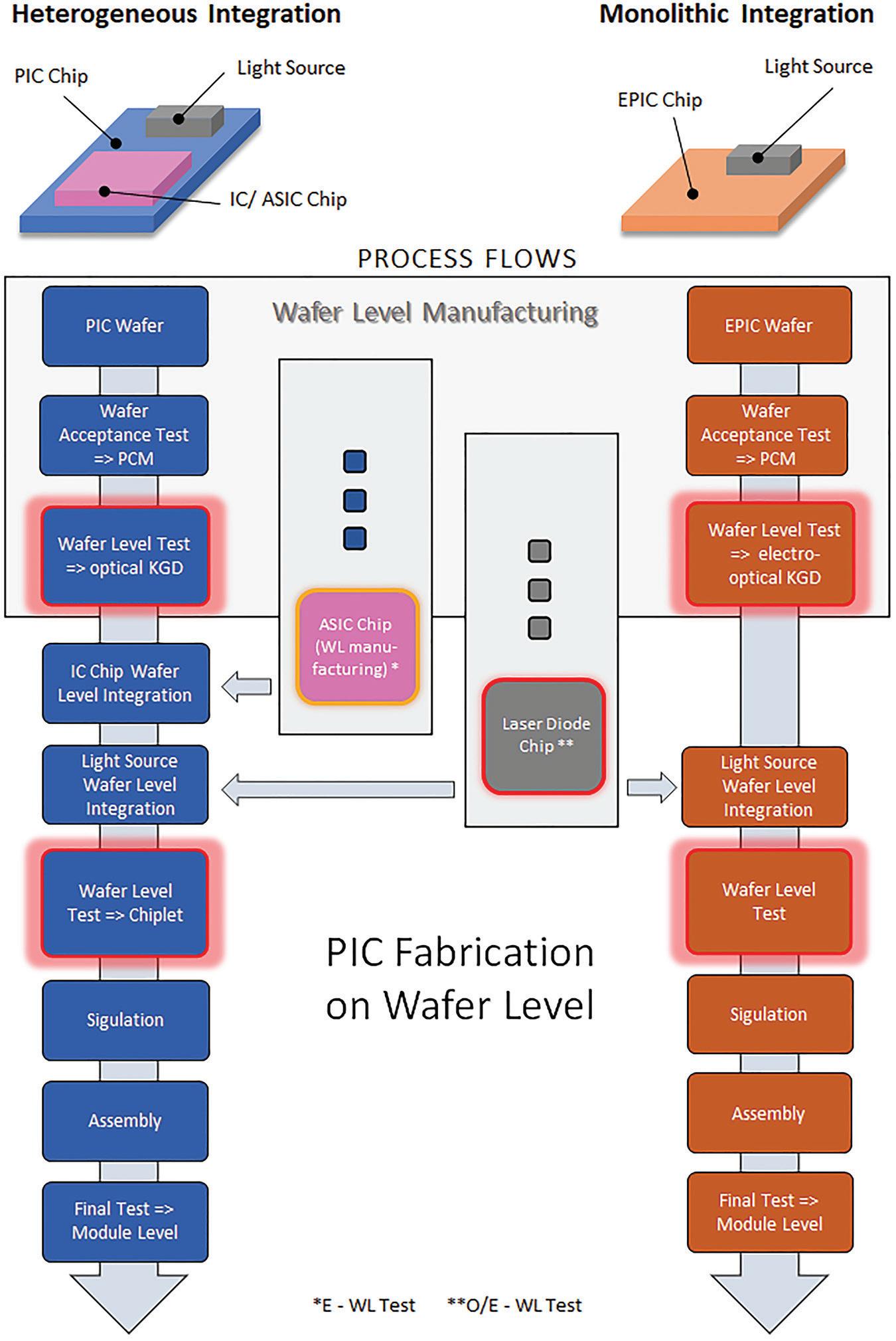
Depending on the type of integration of the PICs, testing takes place at different points in the wafer manufacturing chain (Figure 1). Looking at heterogeneously integrated PICs, the optical wafers, and the driver chips (ASICs) have their own individual manufacturing chain and thus also wafer tests. For monolithic-assembled PICs the electronics are already integrated into the chip. Here, wafer-level tests are crucial. Wafer maps with known-good-dies (KGD) provide information about the quality of the chips at an early stage and identify rejects.

II. Novel Test Concept
With the Jenoptik´s UFO ProbeTM Card, a different test approach was pursued. Here, an optical and an electrical probe module are monolithically integrated to a single probe card. The patented technology includes an optical concept which does not require active alignment of the optical interfaces for each die. Previous technical limitations, such as different position tolerances of optical and electrical components, can be overcome and it can be used like an ordinary electrical test card on existing IC Test equipment like standard probers. In this way, it enables time-saving parallel testing of optical and electrical components on chips. With this monolithic approach a multiple device under test (multi-DUT) testing scheme is also possible.
III. Structure of the probe card
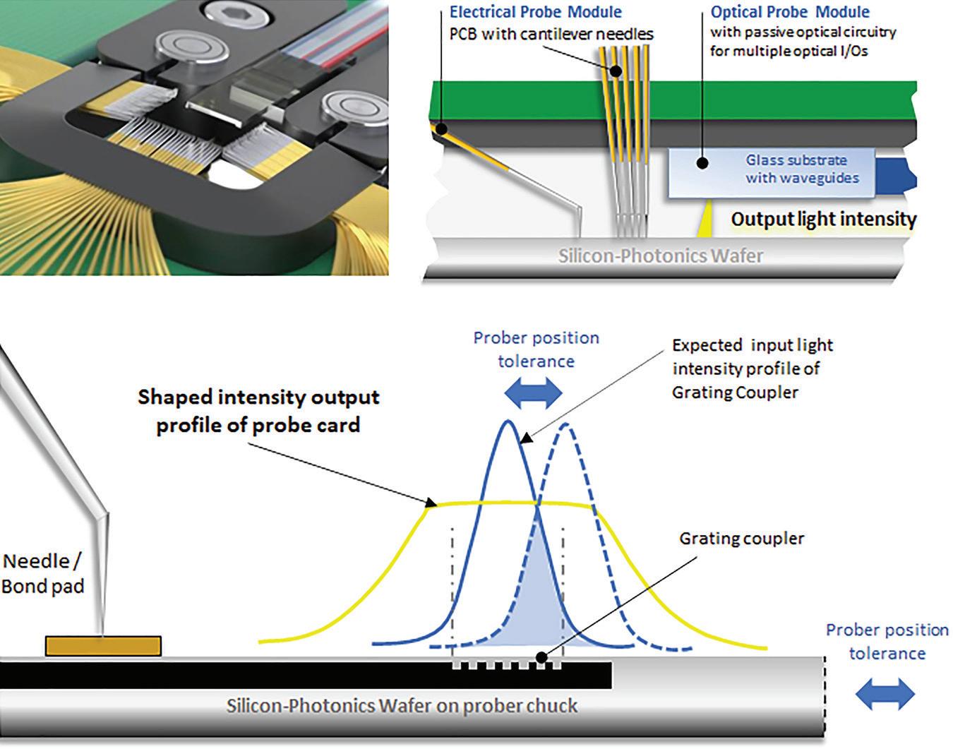
The standard design of the UFO ProbeTM Card is based on the Eurocard format. The stiffener is designed to fit into the corresponding probe interface, in this case a 4.5” standard size. The optical module is shown in Figure 2. It is fully integrated into the probe card and has a defined positional relation to the needles, which is determined by the chip layout.
The optical module – the core component of the probe card – is monolithically constructed of glass and contains up to 32 waveguides and micro-optics for beam guidance and shaping. The standard pitches of the linearly arranged optical channels used are 250 µm and 127 µm. The exit angle of the light lies typically between 10° and 12° in air to serve the currently used transceiver interfaces. However, the angle can be freely adjusted between 0° and 20° in the design. The waveguides and optics are optimized for the wavelength range of 1310 nm (O-band) and 1550 nm (C/L-band).
The optical module can be combined with different needle technologies, such as cantilever or vertical needles. Here, the established technology of well-known probe card manufacturers, such as htt Group or MPI Corporation, is used. A capacitive distance sensor is integrated to monitor the actual working distance of the probe card during operation.
IV. Working Principle
The test card is designed for verticalemitting PICs. Edge-emitting PICs are not served by the current optical concept. The key point here is that the optics, which require a very high alignment tolerance, must also compensate for the coarser accuracy of the prober. The common procedure would be to match the intensity distribution of the grating coupler (mode profile) to the mode profile of the optical fibers that are used as coupling device. Usually, the mode profile represents a Gaussian-shaped intensity distribution (see Figure 2). If the prober now continues to step from one chip on the wafer to the next, a relative change in the position of the grating coupler can occur due to fluctuations in the positioning of the wafer in the prober. The Gaussian profile is now in a different position and only the overlap between the expected and the real intensity profile is coupled into the grating coupler. Thus, the intensity value decreases, and a significant measurement error is obtained. This results in the already mentioned high requirement for positioning accuracy in the sub-micron range, which is typically achieved by time-consuming active alignment.
With the novel UFO ProbeTM Card, the optical coupling points on the chip are overframed to a certain extent. This over-framing (Figure 2) ensures constant coupling conditions and thus a constant measured value over a large lateral range. In the simplest case, this can be a larger Gaussian profile. Ideally, the over-framing is realized by a top-hat-shaped beam profile, that is especially design to the coupling conditions of the grating coupler and stabilize the alignment insensitivity even further.

The disadvantage of the method is the lower coupling efficiency compared to mode matching. Due to the over-framing, all light outside the grating coupler is lost, which leads to a higher insertion loss, but in favor of repeatability. With standard grating couplers, the coupling loss can be as high as 8 dB in some cases. However, it is always possible to select the parameters of the coupling beam to achieve a desired optimum between measurement accuracy, coupling efficiency and position independence. In the case of dedicated coupling points for pure measurement purposes (design for test), mode matching can also be carried out here and the coupling losses are minimized.
V. Application in the field
This probe card is in use in the field with various customer wafers and is used on stan- dard wafer probers, such as the Accretech UF3000EX. Tests are being carried out under real conditions.
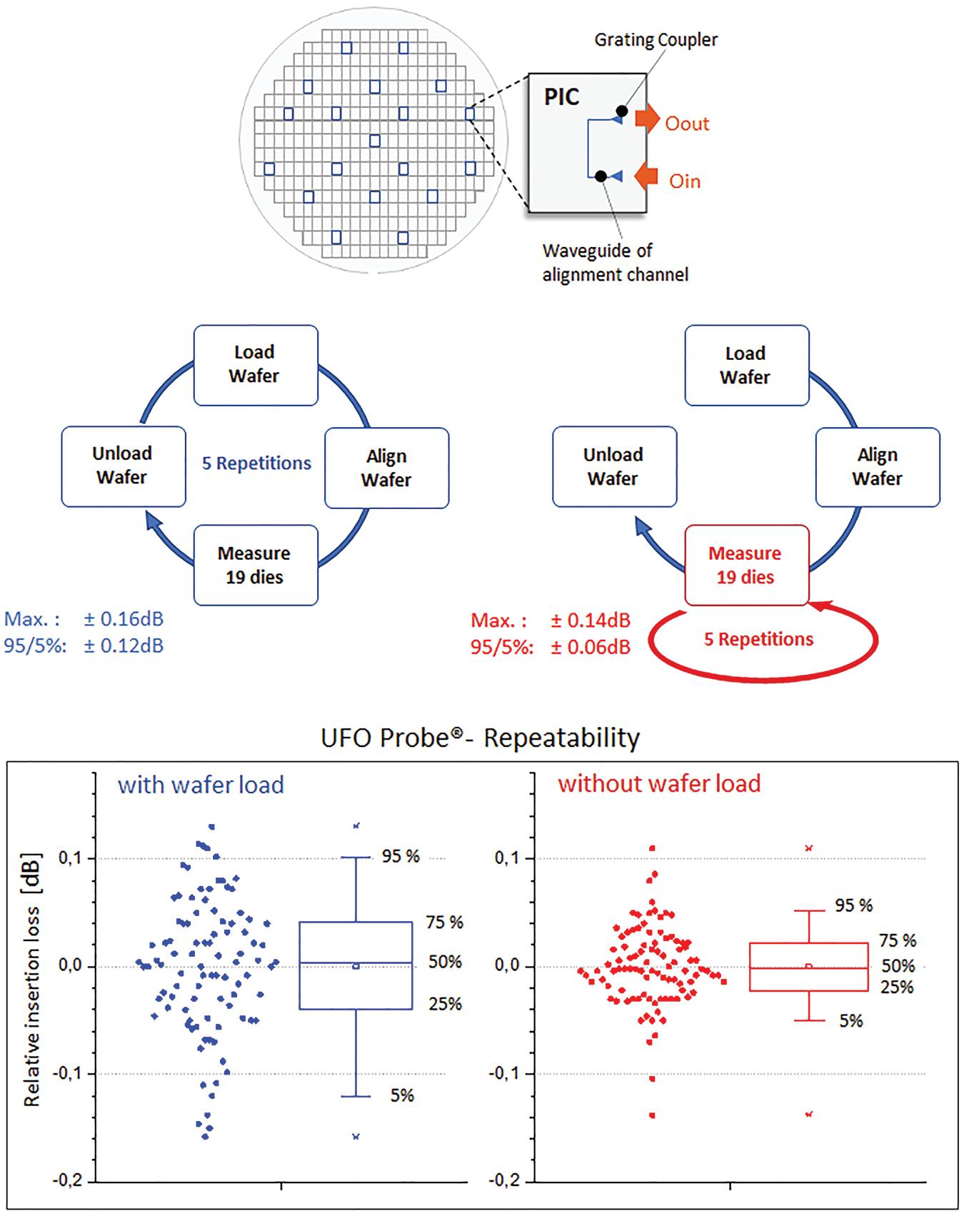
The influence of selected prober functions on the measurement accuracy was also evaluated on a test wafer (Figure 3). For this purpose, 19 defined dies distributed over the entire wafer were measured five times. The PICs were contacted both electrically and optically. For the considerations here, however, only the measurements of the insertion loss at an optical alignment channel were evaluated. In the first test scenario, the wafer was aligned in each run (Figure 3). The change of the recorded insertion loss (IL) was within +/-0.16 dB, while 90 % of the measured values lay within +/- 0.12 dB.
In the second test scenario, the measurement was carried out without reloading and aligning the wafer. It was only loaded once, aligned, and then measured with the corresponding repetitions. The maximum spread of IL change decreased to +/-0.14 dB, while the 0.05 and 0.95 percentiles decreased to +/- 0.06 dB.
This shows that the initial sample-to-pad alignment of the prober has an important influence on the reproducibility of the measured values.
VI. Prospects
Beyond the standard configuration of the UFO ProbeTM Card described above, the technology is currently being developed further to the extent that more than 32 optical channels can be contacted simultaneously. And this in such a way that these can also be arranged in a configuration other than the linear configuration, also in a multiDUT configuration. With the use of vertical needles, the PIC test is possible in the GHz range. For the extension into the upper GHz range, the integration with the corresponding needle types as well as the adaptation to the interfaces of automatic test equipment will be evaluated.
Summary
The novel UFO ProbeTM Card technology is to be seen as a complement to already existing test solutions and is especially designed for PIC wafer-level tests in highvolume manufacturing and with high test throughputs. This is guaranteed by the probe card’s optical concept and its simple integration into existing IC test and probe equipment. ◆


Author Biography


Tobias Gnausch is Product Manager at Jenoptik for the ‘UFO ProbeTM Card’, a new device for PIC wafer-level testing. He joined Jenoptik as an optical designer for diffractive optical elements and systems. He also worked for Bosch as a mechanical engineer and developer for interferometric stylus measurement systems. Tobias studied technical physics and holds several patents in the field of testing as well as micro-optics.
References
[1] C. R. Doerr, “Silicon photonic integration in telecommunications”, Front. Phys.3:37, 2015.


[2] B. Moyer, “Testing Silicon Photonics In Production”, Semiconductor Engineering, Testing Silicon Photonics In Production (semiengineering.com), 2021.

[3] UFO Probe Card, Jenoptik, https://www.jenoptik. com/products/optical-test-measurement-solutions/ ufo-probe-card
[4] B. Tunaboylu , A. M. Soydan, “MEMS Technologies Enabling the Future Wafer Test Systems”, In MEMS Sensors, chapter 58798, http://www.intechopen.com, 2018
[5] J. De Coster, et al., “Test-station for flexible semi-automatic wafer-level silicon photonics testing”, in Proc. 21st IEEE European Test Symposium (ETS), 2016.
[6] C. Dankwart, M. Seyfried, T. Vahrenkamp, “Full automatic test environment for high-throughput PIC testing”, Proc. SPIE 10899, 108990N, 2019.


