8 minute read
Assembly Solutions for Cost-Effective Heterogeneous Integration with Disparate Die Types
from MEPTEC Report Spring 2023
by MEPTEC
Glenn Farris Vice President of Strategic Marketing Universal Instruments

THE SEMICONDUCTOR INDUSTRY is driving to enable high volume integration of disparate die types via Heterogeneous Integration. These die can come from a range of wafer sizes fabricated in different technology nodes. This emerging package type creates new challenges regarding assembly efficiency and yield. Traditionally, flip-chip assembly process flows have utilized a single placement tool for the placement of the single die type onto the target substrate. For applications with multiple die types, a series of placement tools have been configured in a production line, with each tool dedicated to placing a specific die type. This paper explores the implications of this type of solution in the era of Heterogeneous Integration. Impacts on product yield, throughput, manufacturing efficiency, and overall assembly cost will be explored for a broad range of Heterogeneous Integration die configurations. A novel approach to optimizing overall assembly economics will be proposed based on sensitivity analysis for the range of die types expected in these applications. The appropriateness of this novel approach will be explored for a range of packaging solutions, including Flip-Chip, 2.5D, 3D, and Fan-Out.
Introduction
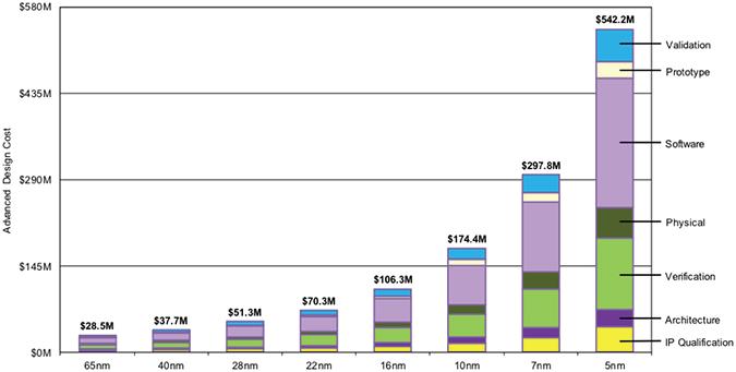
While transistor scaling continues, the economic improvements derived from this scaling, typically referred to as “Moore’s Law,” have been diminishing. For example, over the past decade, at nodes below 22 nm, the associated costs to design and introduce new products have increased by a factor of 7.75. (Figure 1,[1]).
The prevailing packaging solution to address this challenge is called Heterogeneous Integration (H.I.). Many studies have focused on areas such as chip to chip signaling, power distribution, materials, thermals, bonding metallurgy, and design methodologies. Interface open standards such as UCI Express [2] attempt to establish a common specification for H.I. implementation.
However, the economic implications for various placement tool process flow have not been assessed. Placement tool costs can be subdivided into five major categories: yield, equipment depreciation, operators, floor space, and equipment utilization.
The “pick and place” assembly of multiple disparate die in a heterogeneous integration package traditionally uses multiple placement tools. Each unique tool is dedicated to placing a specific die type and/or wafer type. A novel approach is to execute the complete placement of all die types for a given Heterogeneous Integrated package within a single tool. As such, a sensitivity analysis for a broad range of die configurations can be assessed by modeling the impact on the five major cost categories for multiple dedicated placement tools versus a single tool solution.
H.I. Circuit Characteristics
Device Types and Quantity per Substrate
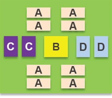
The number of devices per H.I. circuit ranges from a minimum of two device types and may be as high as eight unique devices. These die typically range in size from 0.5 x 0.5 mm up to 20 x 20 mm. The quantity of each die per substrate can range from one to as many as eight.
Each die has a specific function, ranging from processor to memory, to sensing, to data transmission. A typical configuration with four die types and a maximum of eight die for one die type is shown in Figure 2.
Substrate Size and Quantity
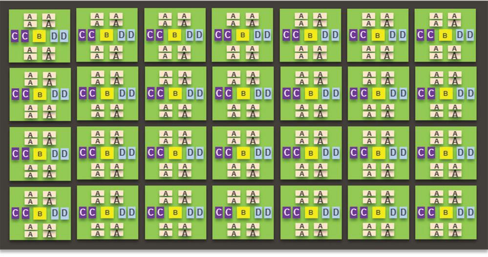
Substrates upon which devices are mounted can range from traditional singulated high-density interconnect (HDI) organic to singulated silicon interposers to a substrate-less Wafer or Panel fan-out. In the case of singulated organic substrates, these are typically presented to the “pick and place” assembly tool via a JEDEC standard tray (or Gen2 JEDEC tray in the future). At substrate dimensions up to 31 x 44mm, up to 28 circuit substrates can be loaded in one JEDEC tray (Figure 3). Future Gen2 JEDEC trays can hold up to 56 of these sized circuit substrates.
A substrate-less Wafer level fanout carrier offers an assembly area for approximately 38 of this sized circuit. In contrast, a JEDEC standard panel fan-out carrier with a 600mm x 600mm assembly area supports up to 247 of this sized circuit.
The number of circuits per carrier significantly impacts the throughput of a single-cell placement solution, as wafer exchange time is amortized over a much larger number of placements for a specific die type. (Table 1)

Pick and Place Tool Characteristics
Traditional die pick & place line solutions have been optimized based on the premise that a single die will be placed on a single substrate. This is the typical flipchip application, which is the dominant “advanced packaging” application in the market today.
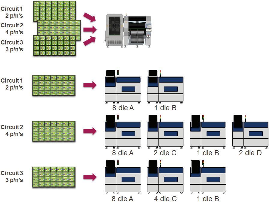
In the case of Heterogeneous Integrated devices, the solution has been to configure multiple systems in series with each other. Each system is tooled and dedicated to a specific wafer type and die type. There are several challenges with this approach.
The first challenge is that the line is unbalanced, as some systems may be placing eight or more devices, while some could be placing only one die (or even zero devices if there are more systems than die types to be placed). This results in an overall “effective throughput” per system that is as low as 13% of a single system solution. Constant re-arranging of the line would be required to optimize the assembly flow for different H.I. circuit configurations, which is impractical in a production environment. (Figure 4)
The second challenge is that the constant flattening and then flexing of the substrate can cause die float, as can movement out of and into multiple systems, impacting placement accuracy. Finally, moving substrates between eight dedicat- ed systems in a line increases placement, fiducial find, and potentially temperature variability, further degrading placement accuracy. Based on typical system variability data, it is estimated that all these factors will increase the defective place- ment parts per million (ppm) per device from a typical value of 100 ppm to 400 ppm for a 4-die H.I. device.
The third challenge is that increased operator attention will be required per line with up to eight machines in a line, as will increased floor space. This will increase the overall operational expense (OPEX) cost for the line proportional to the number of systems in the line.
The fourth challenge is utilization. Creating dedicated lines per circuit configuration versus a single cell that can handle any circuit will reduce typical utilization. In addition, material scheduling and downtime typically reduce a singlesystem solution to 85% utilization. With a 4-system solution, these “multi-system” factors are expected to reduce utilization further to, at best, 60%.
Throughput Sensitivity Analysis
To better understand the overall impact of these various parameters on Heterogeneous Integration assembly economics, a mathematical model was created to allow for a comprehensive sensitivity analysis.
As mentioned, the most critical factors are the time it takes to automatically change wafers and change associated end effector tooling to support a new die type, the number of circuits to be assembled per carrier, and the number of unique die types to be assembled per circuit.
Impact of Circuits per Carrier and Wafer & Tooling Change Time
Table 2 summarizes the relative throughput of assembled circuits for a Single System per Circuit solution vs. a Single Die per System solution. The comparison is made both for a Single System solution configured with a single wafer table as well as a Single System solution configured with dual wafer tables. The time to exchange unique wafers and end effector tooling (used for picking up the individual dies) for unique die types was varied from 15 seconds to 60 seconds. For this example, it was assumed the circuit had four unique die types, with quantity of die per die type of 8, 4, 2, or 1 respectively.
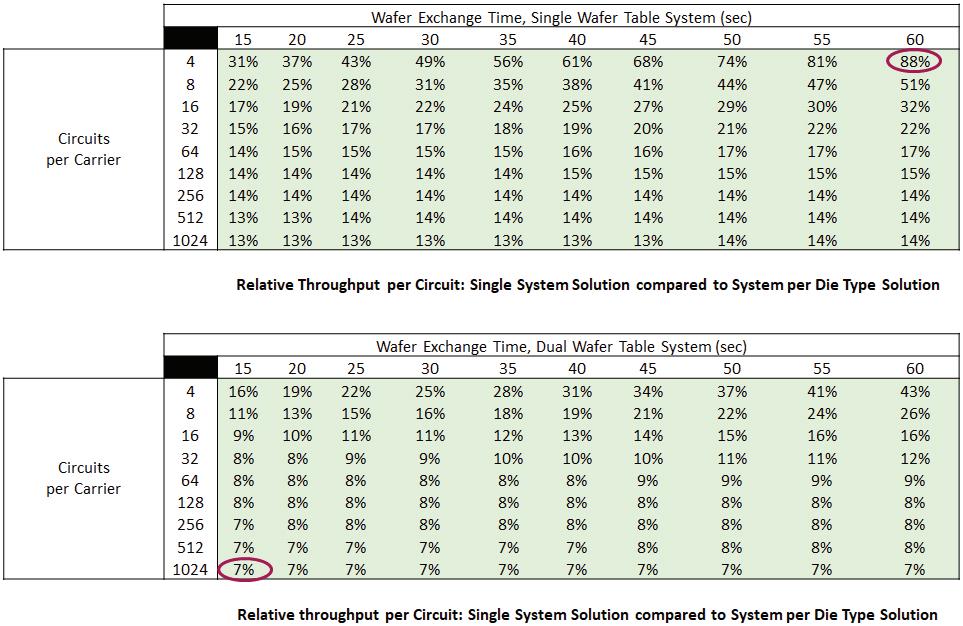
From Table 2, it can be seen that over the full range of scenarios for circuits per carrier and wafer + tooling exchange time, a Single System per Circuit solution delivers superior throughput. This advantage ranges from 12% in the corner case of only 4 circuits per carrier and 60-second wafer + tooling exchange time on a Single Wafer Table system up to
93% advantage when there are 1,024 circuits on a carrier and an exchange time of only 15 seconds.
Impact of Number of Die Types and Counts per Circuit
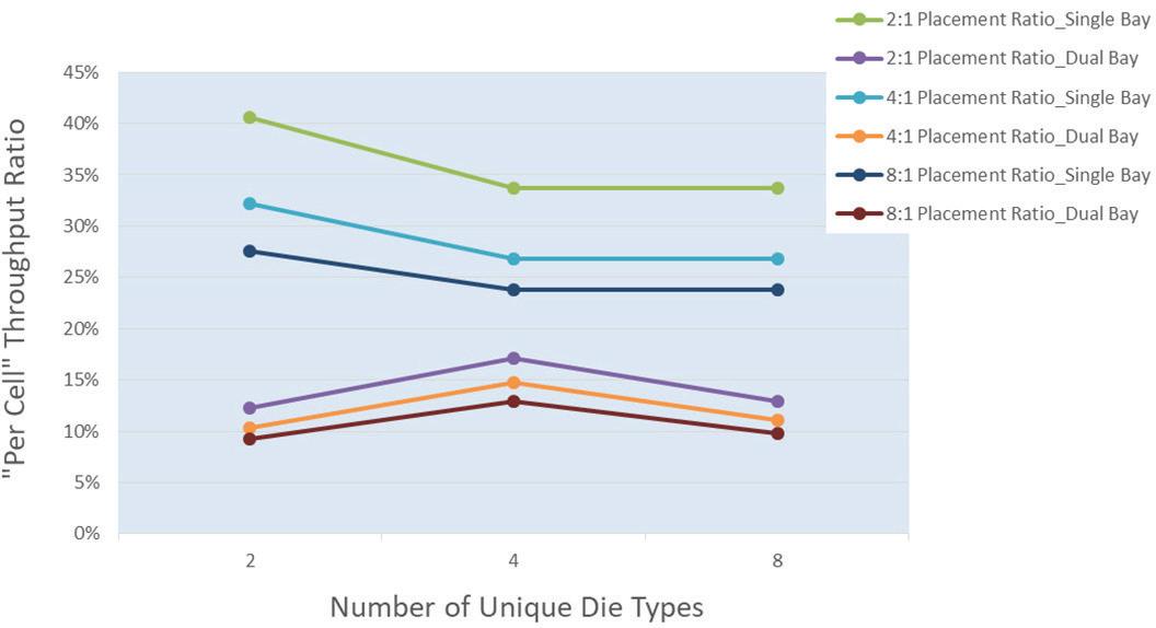
The impact of the number of unique die types per circuit and the quantity of each die type on the relative throughput of each solution type was also analyzed. This analysis was done for a fixed number of 28 circuits per carrier and a 30-second wafer + tooling exchange time.
As shown in Table 2, a Dual Table system, on average, doubles the relative throughput of a Single Cell per circuit solution. Generally, the placement speed doubles and the time spent exchanging wafers + tooling is cut in half, resulting in this improvement. The Single and Dual Table Single System per Circuit solutions exhibits a 60% to 90% improvement in throughput in this example.
Secondly, the overall variation from 2 to 4 to 8 unique device types has much less impact than the number of circuits per carrier noted in Table 1.
Finally, the relative quantity of each unique die type has a more significant impact than the number of unique die types, mainly due to a greater impact on the total number of die on the circuit.
(Figure 5)
Economic Model Summary
An economic model was created to assess the economic impacts of yield, depreciation per circuit, OPEX, and utilization. Pricing for a single wafer table Single System per Circuit solution was arbitrarily set to one million dollars. The price per machine for the single dedicated system per die type solution was set at $500 K.
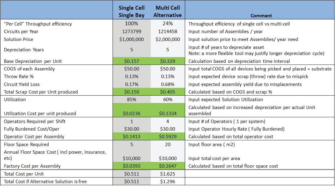
A key observation from the economic model is that, while depreciation cost per assembled circuit is the typical factor used for solution comparison, the assembly yield has a much larger impact on the overall cost of manufacturing. (Table 3)
For the single bay Single System per Circuit solution, the depreciation cost is only 30.7% of the total assembly cost.
Two other factors heavily influence total assembly cost: total scrap per unit produced and operator cost. Operator cost is assumed to be directly proportional to the number of systems. Based on an estimated increase in defective placements from 100 ppm to 400 ppm for a four-die H.I. device, the increased scrap cost for the multi-system solution is more than the depreciation cost for the Single System per Circuit solution.
The economic model shows that even if the multi-system solution is free, the increased scrap, operator, and utilization costs result in the single-system solution delivering a 60% lower overall assembly cost.
Conclusion
In conclusion, with the advent of high-volume Heterogeneous Integration circuits, efficient advanced packaging assembly solutions are critical to optimizing the overall economics. A comparison of traditional assembly processes, which require a dedicated assembly system per die type, to a novel solution utilizing a single assembly system for all die, demonstrates a 60% cost of assembly advantage for the single-system solution. ◆
Author Biography
Glenn Farris joined Universal in 2013 as Vice President, Marketing and has been instrumental in leading the company to develop a strategic relationship with some of the world’s most prominent technology leaders. Glenn holds an MBA in Marketing and Finance from Santa Clara University, M.S. in Engineering from Stanford University, and a B.S. in Engineering from Purdue University. Email: glenn.farris@uic.com
Acknowledgments
The author wishes to acknowledge this novel solution’s inventors and patent holders: Mike Yingling, Sean Adams, David Lyndaker & Scott Proctor – all employees of Universal Instruments.[3]
References
[1] IBS. As Chip Design Costs Skyrocket, 3 nm Process Node Is in Jeopardy. 2020. Available online: https://www.extremetech. com/computing/272096-3nm-process-node
[2] UCIe 1.0 Specification is an open industry standard developed to establish a ubiquitous interconnect at the package level. Available online: https://www.uciexpress.org/specification
[3] High-Speed Wafer Feeder Patent Number: 11164765 Issue date: 11/2/2021
Title: Modular Die Handling System
Inventors: Mike Yingling, Sean Adams, David Lyndaker, Scott Proctor


