29 minute read
Research Highlights
July 1, 2019 – June 30, 2021.
Advertisement
Due to the non-publication of the 2020 hard copy Annual Report because of COVID-19 related issues, this report will showcase research highlights from the two-year fiscal periods, July 1, 2019 – June 30, 2021.
Energy Storage
Energy storage to enable the next generation of mobile devices, homes and transportation is a pivotal part of a future sustainable energy society. Batteries have long provided a means to enable mobility and since the inception of lithium-ion batteries, researchers have focused on finding materials and processes to reliably and affordably introduce them into a range of applications. Solid-state batteries, where the liquid electrolyte and polymeric separator between the positive and negative battery electrodes are replaced with a solid-state lithium-ion conductor, are primed to accelerate the next generation of solid-state-based energy storage applications. One key driver for solidstate batteries is the conductivity of the solid-state electrolyte; playing the pivotal role of fast lithiumion conductor while maintaining a robust electrical separator between the positive and negative battery electrodes. Hence usually, better the conductivity of the solid-state electrolyte, better the performance of the solid-state battery. One recent avenue of conductivity enhancement for sulfide-based solid-state electrolytes being studied by researchers has been the incorporation of halide-based materials to them. However, a fundamental understanding of the compositional and morphological transformations between halide-incorporated and pure sulfide-based solid-state electrolytes during battery cycling has been absent from the scientific literature. This is because of the challenges associated with the availability of techniques capable of probing these materials with nanoscopic spatial and temporal resolutions needed to study such transformations in real time. Transmission electron microscopy (TEM) is established as an essential visualization tool for nanoscale materials, interfaces and reactions. Operando experiments are quickly becoming ubiquitous and accessible to visualize and characterize important scientific processes, such as those occurring during battery cycling.
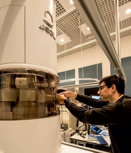
As summarized in the results recently published in the ACS journal Chemistry of Materials (https:// doi.org/10.1021/acs.chemmater.9b05286) we used advanced analytical techniques, such as operando TEM in the solid-state amongst others, to understand the influence of halide-based materials on the performance of certain solid-state electrolyte materials. The implementation of operando TEM to assess the chemomechanical interface of the solid electrolytes during real-time battery operation within the TEM allowed us to identify potential performance failure mechanisms in solid-state batteries. All the TEM work summarized in our results was conducted at the Singh Center for Nanotechnology at the University of Pennsylvania on the JEOL JEM-F200 microscope.
This work was made possible through the unique development of special sample preparation and microscopy procedures necessary for sulfide-based and halide-incorporated solid electrolyte materials utilized in this study, which in turn enabled the collection of such “first-of-a-kind” data. This serves as a fine example of how continuous improvement of operando visualization techniques, specifically electron microscopy, accelerate fundamental discoveries towards realizing practical energy storage solutions.
This work was led by Toyota Research Institute of North America researchers Dr. Nikhilendra Singh, and Dr. Timothy S. Arthur, and collaborated upon at the Singh Center for Nanotechnology at the University of Pennsylvania by Professor Eric A. Stach and his graduate student Mr. James P. Horwath. The authors gratefully acknowledge use of facilities and instrumentation supported by The National Science Foundation through the University of Pennsylvania Materials Research Science and Engineering Center (MRSEC) (DMR-1720530).
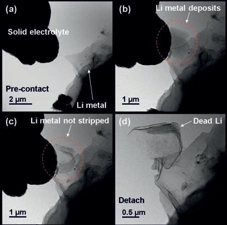
Right: Bright-field STEM images taken on the JEOL JEM-F200 microscope at the Singh Center for Nanotechnology highlighting the implementation of operando TEM to assess the chemo- mechanical interface of a solid electrolyte in contact with lithium (Li) metal during electrochemical operation.
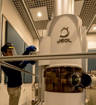
(a) Prior to electrochemistry (b) deposition of Li (c) stripping of Li (d) post electrochemistry where the presence of dead Li suggests a potential failure mechanism for such a battery. The JEOL JEM-F200 microscope.
SARS-CoV-2 Research
The global pandemic of COVID-19, the disease associated with severe acute respiratory syndrome (SARS-CoV-2) infection, has caused over 650,000 deaths, millions of confirmed infection cases and billions of influenced people. Rapid, accessible and sensitive diagnosis of SARSCoV-2 infection is critical for preventing the transmission of the disease. However, rt-PCR, the currently widely used testing technology for screening and diagnosis of patients with suspected COVID-19 syndromes, has a typical turnaround time over 24 hours. Although serology tests can be performed more rapidly, their sensitivities are limited, postponing a detectable signal by days to weeks after symptom onset. To answer this problem, researchers at Penn have leveraged the microfabrication capabilities at the Singh Center to fabricate microbubbling microchips and develop a microbubbling digital assay for the early diagnosis of COVID-19 by detecting SARS-CoV-2 nucleocapsid protein (N-protein) from respiratory swabs.
This microbubbling digital assay, which was based on a recently published work (Angew. Chem. Int. Ed. 2019, 58, 13922 – 13928), has the potential to be rapid (<1 h), RNAextraction-free, smartphone accessible and ultrasensitive (with rt-PCR-comparable sensitivity). In the microbubbling digital assay picolitre-sized microwells together with platinum nanoparticle labels enable the discrete “visualization” of SARS-CoV-2 N-protein molecules via immobilized-microbubbling with smartphone camera. We also used computer vision and machine learning to develop an automated image analysis smartphone application to facilitate accurate and robust analysis of the assay results. These systems are currently being validated with clinical samples and will be integrated into lab-on-a-chip devices with automated washing, signaling, reading and data processing. Once the integrated devices are delivered, the diagnostic process of COVID-19 could be greatly simplified and shortened, improving the control and prevention of the transmission of COVID-19.

This research was performed by Hui Chen and Ping Wang of the University of Pennsylvania’s Department of Pathology and Laboratory Medicine.
Funding for this project was provided by the Penn Center of Precision Medicine, Penn Health-Tech and Penn Center for Innovation and Precision Dentistry.
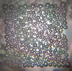
This image shows microbubbles generated by inactivated SARS-CoV-2 viruses on our chip.
Tunable Topological Charge Vortex Microlaser
In the digital era of proliferating connections between pervasive endpoints, the tremendously growing aggregated data traffic motivates the development of innovative optical communication technologies to sustain the required massive increase in information capacity. The current information infrastructure based on wavelength and time division multiplexing, together with other degrees of freedom of light including the amplitude, polarization and phase, is, nevertheless, approaching a bottleneck. Fortunately, the full-vector nature of light provides another information dimension, namely the orbital angular momentum (OAM) to ease the upcoming information crunch.
The ongoing effort of OAM-spin-wavelength division multiplexing for multi-dimensional high capacity information processing requires the flexible generation and versatile manipulation of different OAM and spin states at the same wavelength to fully take advantage of the orthogonality of OAM modes, which is not yet accessible by state-of-the-art microscale devices. Here, to overcome this longstanding challenge, we exploited the spin-orbit coupling, based on the conservation of the sum of the OAM and transverse spin, to precisely maneuver the chiral light states in microring lasers. The ability to simultaneously and cohesively manipulate both the SAM and OAM degrees of freedom can couple the local spin with orbital oscillation of optical cavity modes, thereby leveraging richer functionalities in vortex light generation. Our tunable vortex microlaser is capable of emitting vortex beams of 5 different topological charges at room temperature. The toolbox of generating various vortex light at a single wavelength holds the promise for future development of multi-dimensional OAMspin-wavelength division multiplexing for high-density data transmission in classical and quantum regimes. Additionally, dynamic switching between different OAM modes in time can further increase the security of wired and wireless communication networks.
This research was performed by Liang Feng of the Penn Departments of Materials Science and Engineering and Electrical and Systems Engineering, Ritesh Agarwal of Penn Materials Science and Engineering, Natalia M. Litchinitser, and Jingbo Sun at Duke University, Josep M. Jornet at Northeastern University, and Stefano Longhi at Politecnico di Milano.
Academic Research To Startup: Nanoscale Pores For Dna Sequencing Precision drilling of nanopores in silicon suspended on glass chips for DNA sequencing has been carried out with our Transmission Electron Microscopes. The nanopore diameter is in the range of 1-2 nm (for comparison, a single stranded DNA molecule is 1.1 nm in diameter) and the measurement error of +/- 0.1 nm. The membrane thickness is about 3 to 5 nm, monitored in situ by the electron energy loss signal. Error! Reference source not found. shows a schematic drawing of the nanopore device. The image in Error! Reference source not found. shows an electron microscope view of one of these pores. A publication of this work is in preparation. Prof. Marija Drndic’s lab at Penn conducted this research.
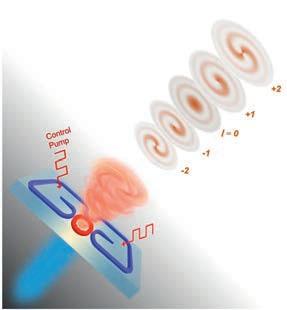
Schematic of non-Hermitian controlled vortex micro-laser. The non-Hermitian interaction mediated by the externally applied control pump on the bus waveguide can flexibly be switched for the emission of OAM states with desirable chirality from the spin-orbit engineered micro-ring.
Nano IoT: A Hybrid Integrated Artificial Mechanoreceptor in 180 nm CMOS
5.4 million people in the US suffer from paralysis, which disrupts the communication between the brain and body. As a result, the patients suffer from a loss of muscle function and sensation. To restore the sense of touch to a paralyzed hand, we introduced a sensorbrain interface that performs tactile sensing using an artificial mechanoreceptor device, then the detected force information will be encoded to the brain using a neural stimulator.
The proposed artificial mechanoreceptor includes a custom capacitive tactile sensor and an interface integrated circuit (IC). Wireless power and data links are realized through magnetic human body communication. The device is low power and implantable. A base unit worn on the wrist, which includes a primary coil, will be used to generate the wireless power and collect data from the implant.
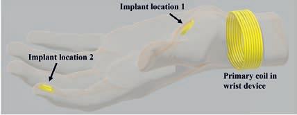
Top: The proposed tactile sensing system. Middle and bottom: Sensor assembly diagram.
A capacitive tactile sensor based on fused silica is developed. The sensor includes a silica upper plate with a cavity and a circular electrode as well as a silica substrate with two semi-circular electrodes, feedthroughs, and pads underneath. A localized fusion bonding of the upper plate and the substrate is achieved by carbon dioxide laser-assisted technology. Thus, the top circular electrode and the two semicircular bottom electrodes could be equivalent to two semi-circular capacitors in series connected by the top electrode. In the presence of normal force, the upper plate deflects toward the substrate, decreasing the distance and increasing the capacitance.
The testing circuit includes an application-specific integrated circuit (ASIC) chip with a resolution of 22.8 fF over an input range of 100 pF for measuring capacitance of this sensor prototype. The proposed chip is implemented in a 180nm standard CMOS process. The total area including bond pad is 1.6 mm2 and the chip power consumption is 104 µW.
The proposed artificial mechanoreceptor device is characterized on a dynamic loading analysis system. Both static and sinusoidal loading/unloading can be detected by the device. The artificial mechanoreceptor exhibits good repeatability.
This research was performed by Han Hao, Lin Du, Andrew G. Richardson, Timothy H. Lucas, Mark G. Allen, Jan Van der Spiegel, and Firooz Aflatouni, University of Pennsylvania.
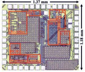

Top: Chip microphotograph. Bottom: Sensor prototype on a gloved index finger.
Mobil-Aider Device External User Research – Startup - Therapeutic Articulations, LLC
With the assistance of a Phase II National Science Foundation grant and funding from Ben Franklin Technology, the development of the Mobil-Aider device to measure joint mobility continues in spite of the environmental impact of COVID-19. Changes to the housing of the device and preparation for injection molding has resulted in the use of an over-pour technique to the various attachments. This will allow for excellent contours with an easily cleanable material. The reconfiguration of the docking station will simplify assembly and reduce cost.
The reliability and validity of the measurements via bench and clinical testing has been confirmed. The Zeiss Smartzoom microscope, located at the Singh Center of Nanotechnology (University of Pennsylvania), was used as the gold standard to assess the ability of the Mobil-AiderTM to measure linear translation. Sixty blinded measures were taken with each of six different Mobil-AiderTM devices. ICC & Pearson correlation = 0.986, indicating a strong correlation between the measures. Cronbach alpha reliability analysis = 0.992. Independent one-sample t-tests were performed on the differences between the Mobil-AiderTM and the Zeiss values (p = 0.42), indicating the measures were not statistically different. Bland Altman plot and a linear regression revealed no proportional bias.
Professor Dawn Gulick, of Widener University, says, “Orthopedics is about precision. The Mobil-Aider device is able to quantify knee joint laxity to contribute to the clinical decision-making regarding injury management and the ability to quantify joint mobility to consistently render therapeutic treatments to improve quality of care. Mobil-AiderTM represents a 'first-to-market' technology for arthrokinematic/linear assessment.”
In addition, a case report using radiographs to assess linear translation of the knee with the Mobil-AiderTM revealed interesting information. A radiographic image was taking in anatomic neutral and at end-range of an anterior tibial translation, i.e. Lachman test. The delta of the tibial position measured 6.9 mm of anterior tibial translation on the radiograph and 7.1 mm on the Mobil-AiderTM LED display. This is a difference of only 2%. Further clinical testing has begun on individuals with anterior cruciate ligament (ACL) injuries. Although only four subjects have been examined, comparisons of the measured laxity with the Mobil-AiderTM device with MRI results are positive.
This research was performed by Dawn Gulick, Widener University.

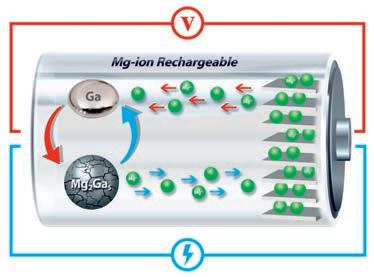
Self-healing Liquid Metal Electrode Extends Life of Mg-ion Battery
Rechargeable lithium-ion batteries (LIBs) have become nearly ubiquitous in our daily lives: they power our portable electronics, store solar energy, and, especially in recent years, put electric vehicles on the road. Unfortunately, the increased demand for batteries has placed a considerable strain on lithium and cobalt resources, which are becoming more expensive due to increased demand and are supplied by countries with high geopolitical risks. To mitigate these issues, rechargeable magnesium-ion batteries (MIBs) are emerging to support LIBs. There is a major barrier to the widespread adoption of the MIB, however: the anode material typically fails as a result of cracks and pulverization caused by significant volume variation during a solid-solid phase transformation as Mg ions are incorporated into the crystalline host material to store charge. In our work, we address the cracks and pulverization by employing gallium, a metal that has a melting point a few degrees higher than room temperature, as the anode material.
In this study, we used micron-sized Mg-Ga solid alloy particles, which underwent a solid-liquid phase transformation as Mg was reversibly removed and incorporated at 40 °C. The material is tied into a network of carbon fibers, carbon black and graphene, which held together the active material as it changed phase from crystalline solid to amorphous liquid. We confirmed that the anode makes these changes reversibly during operation by probing its crystallographic changes using in situ wide-angle X-ray scattering (WAXS). This phase change significantly reduces the accumulation of stress within the anode, which we found from finite element simulations. Noting these findings, we argue that the material self-heals using this transformation, preventing the detrimental pulverization that would normally arise during a solid-solid phase change.
This new type of liquid anode material significantly shifted the state-of-the-art in MIBs, outpacing the longest MIB cycle life on record by approximately five times: ours cycled over 1000 times at a higher charge-discharge rate. In addition, there is no need to synthesize the nanomaterials, which are complex, and in many cases non-practical. These characteristics can make MIBs very suitable for industrial applications, making at-scale commercialization possible.
This research was performed by Lin Wang, Samuel S. Welborn, Vivek B. Shenoy, and Eric Detsi, Department of Materials Science and Engineering, University of Pennsylvania.
Ti3C2Tx For High-Density, High-Resolution Electromyography Arrays
High-density arrays of high-resolution electrodes are a valuable tool for recording the electromyogram (EMG), a biopotential representing the activation and coordination of various muscles groups within the human body.
However, to achieve a higher spatial resolution and channel count, smaller electrodes are required, and thus, it becomes challenging to maintain a low interface impedance and a high signal-to-noise ratio (SNR). Carbon-based nanomaterials readily address this challenge by combining a high electrical conductivity with superior mechanical properties and the ability to interface with biological systems without serious concern over biocompatibility.
Nonetheless, it may difficult to fabricate devices from nanostructured carbon, because dealing with these nanomaterials can be expensive and time-consuming. Two-dimensional titanium carbide MXene (Ti3C2Tx) mitigates these concerns. Possessing remarkably high volumetric capacitance and electrical conductivity, as well as excellent mechanical properties and a high degree of surface functionality, Ti3C2Tx is also unique among carbon-based nanomaterials due to its ease of processability in aqueous solutions.
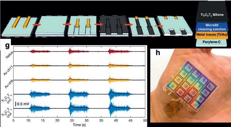
Leveraging these many advantageous properties, we present here a novel microfabrication process for realizing high-density, thin and flexible Ti3C2Tx arrays for surface EMG recording, and demonstrate their superior performance in EMG recordings on healthy human volunteers.
In particular, when compared to >30x larger, gelled silver-silver-chloride (Ag/AgCl) clinical electrodes, our gel-free Ti3C2Tx electrodes still had >100x lower interfacial impedance.
Furthermore, when recording baseline EMG from healthy human subjects, the Ti3C2Tx electrodes demonstrated >4x higher SNR than the clinical-grade electrodes.
We were also able to use the Ti3C2Tx array for tracking the activation and spread of muscle activity on the millimeter-scale over the thenar eminence muscle group of the human hand.
Overall, these results establish high-density Ti3C2Tx MXene arrays for recording high-fidelity, low-noise EMG, with applications in rehabilitation and sports medicine, assistive technologies and basic studies into the mechanisms underlying neuromuscular function and disease. This collaborative project was led by Professor Flavia Vitale of the Penn Department of Neurology, Bioengineering and Physical Medicine and Rehabilitation, and includes contributions from the Penn Department of Physical Medicine and Rehabilitation, the Penn Department of Bioengineering, the Penn Department of Neurosurgery, and the Materials Science and Engineering Department at Drexel University.
Figure. (a–f) The process flow used to microfabricate high-density Ti3C2Tx MXene EMG arrays at the Singh Center for Nanotechnology.
(g) Sample traces of the EMG signals recorded using the MXene array, as compared to a gold array with the same size electrodes, and a clinical-scale gelled Ag/ AgCl electrode. (h) Demonstration of the high-density Ti3C2Tx MXene EMG array for millimeter-resolution recording of muscle activation and coordination over the thenar eminence muscle group of the human hand.
Centimeter-scale Crack-free Self-assembly for Ultra-high Tensile Strength Metallic Nanolattices
Strong and lightweight porous materials are commonly used in industry, but the difficulties in controlling their physical and chemical structures during fabrication have limited their mechanical properties. Nanolattices are porous materials with nanoscale features that promise to overcome these limitations using size-based effects. However, traditional fabrication methods such as 3D printing using two-photon polymerization or self-assembly using nanoparticles, have either limited printing speed or dense cracks in self-assembled lattice templates, limiting characterization of these materials’ properties to be under sub-millimeter scale.
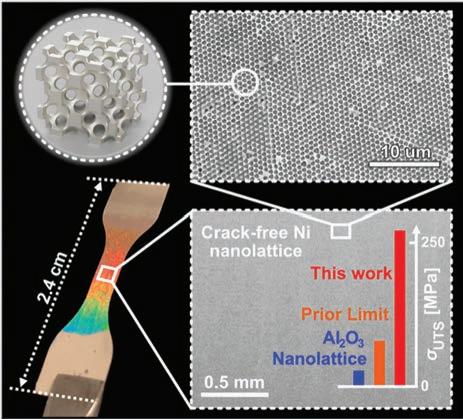
Although many studies have focused on fast fabrication of self-assembled nanolattices, and several have attempted to eliminate template cracks, no selfassembly fabrication approach can produce large-area metallic nanolattices without cracks. To eliminate template cracks and precisely control metallic nanostructure across millions of units to achieve unprecedented properties, researchers at Penn have leveraged the capabilities at the Singh Center to develop a self-assembly method for fabricating centimeter-scale nickel nanolattices without cracks and characterize their tensile properties macroscopically. In the developed crack-free self-assembly approach, the key to eliminating cracks during self-assembly was to keep the template wet with 0.06% glycerol.
Additionally, synthesized positively charged nanoparticles allowed subsequent electrodeposition through the thick, wet opals due to electrostatic forces. The resulting large-area nickel nanolattices had an ultra-high 257 MPa tensile strength, which is 2.6 times the strength of prior porous metals at 0.298 relative density. Moreover, the fabricated nanolattices had excellent photonic coloration, approached the theoretical limit of the upper tensile strength, achieved a combination of strength and relative density that outperformed other porous metals and nanolattices and could resist bending fractures with a lower volume and mass than most porous materials.
The developed methods and findings in this work will further the design and fabrication of lightweight porous metals with the promising combination of high strength, electrical and thermal conductivity, structural coloration, and high specific surface area, which may enhance the performance of many applications such as sensing, high-power-density batteries, efficient heat and mass exchangers and selective infiltration membranes.
This work was conducted by Ph.D. Candidate Zhimin Jiang and his advisor, James H. Pikul of the MEAM Department at the University of Pennsylvania, with funding from the pilot grant Program from the Center for Innovation and Precision Dentistry at the University of Pennsylvania, the National Science Foundation CAREER Grant, the ASME Applied Mechanics Division Haythornthwaite Foundation Research Initiation Grant, and the National Science Foundation National Nanotechnology Coordinated Infrastructure Program (NNCI).
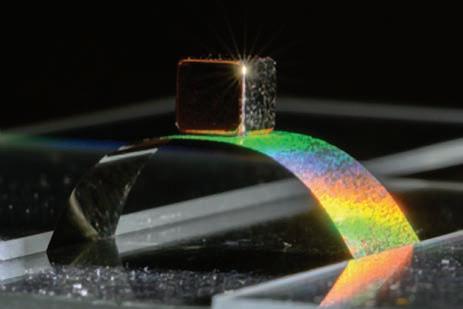
Image one is a bent sample with a load on it. The color of the sample is due to selective reflection from the sample surface.
Image two: A brief summary of the sample properties. The dog bone sample has nanometer scale struts, while it is centimeterscale long with an ultra-high tensile strength compared to other similar materials.
Bile Duct On-A-Chip
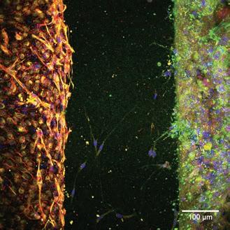
The extrahepatic bile duct (EHBD) transports highly toxic bile from the liver to the intestine. The duct is lined with epithelial cells called cholangiocytes that form a tight and impermeable monolayer and have specialized, bile-resistant apical domains, protecting the duct submucosa and surrounding tissues from bile leakage and associated damage. The bile ducts are targets in multiple diseases in patients of all ages, but their function is not well understood.
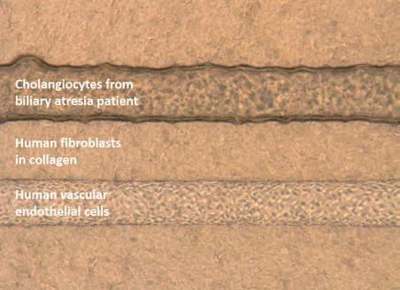
We have used the microfabrication resources at the Singh Center for Nanotechnology to develop a bile duct-on-a-chip and vascularized bile duct-on-a-chip. Both devices contain a perfusable biliary channel lined by polarized cholangiocytes (human or mouse); these channels are remarkably impermeable, with tightness of the monolayer similar to that recorded in vivo. The vascularized bile duct-on-a-chip also includes a channel lined by vascular endothelial cells. The two channels can be perfused independently, with different media at different flow rates, and various treatments can be introduced on either basal or apical sides of the cell layers. Immune cells can be introduced into the vascular channel and will migrate into the intervening matrix, which can vary in matrix composition and be seeded with fibroblasts. The devices are being used to study the impact of biliary toxins on cholangiocyte permeability and function, details of the immune and inflammatory responses to bile duct damage, and the relationship between fibroblasts and cholangiocyte monolayers.
This work was led by postdoctoral researcher Dr. Yu Du and his supervisor Dr. Rebecca Wells in the Department of Medicine at the Perelman School of Medicine, with funding from the NIDDK and the Fred and Suzanne Biesecker Center for Pediatric Liver Disease.
Left to right: Bright field image of vascularized bile duct-on-a-chip with human endothelial cells, cholangiocytes, and fibroblasts. Channels are approximately 160 mm diameter. Vascularized bile duct-on-a-chip with mouse cells, with the vascular channel on the left, biliary channel on the right, and fibroblasts in the intervening collagen matrix, stained for K19, (cholangiocyte marker, green), vimentin (mesenchymal marker, yellow), and VE-cadherin (vascular marker, red); nuclei stained blue.
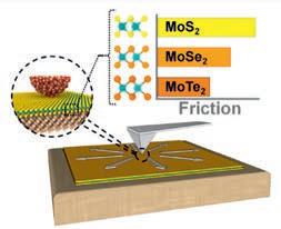
Penn and UC Merced Research Reveals an Unexpected Mechanism Behind Friction for 2D Materials
In a study published in the journal ACS Nano, the team found that the presence of larger atoms within the lattice of a 2D material unexpectedly decreased the friction encountered by the tip of an atomic force microscope probe as it slid along the surface.
In their study, the researchers compared three 2D materials from the same family, transition-metal dichalcogenides (TMD). These materials consist of a metal atom, molybdenum (Mo), bonded to two atoms of one of the chalcogens, the group of elements that include sulfur (S), selenium (Se) and tellurium (Te). Because these elements are all in the same column of the periodic table, they bond equally well with molybdenum and can make 2D lattices with the same overall pattern under carefully controlled conditions.
In its common form as a thick coating, a powder or a suspension, MoS2 is a ubiquitous industrial lubricant, so the possibility of increasing its performance has spurred research into advanced synthesis and manufacturing techniques for it and other TMDs. The authors’ research has been motivated by a desire to better understand the dynamics that govern friction when such materials are in their 2D form, and when their composition is altered.
Based on prior computational results, the researchers expected that selenium and tellurium atoms, being larger than sulfur atoms, would present larger energy barriers for the tip to overcome and thus increase the overall amount of friction. In other words, larger atoms means a “bumpier” road, and thus more friction encountered to move across it.
That expectation was proven to be incorrect. “Other researchers predicted that friction would go up as the size of the chalcogen increased,” says Martini. “But our results show that it goes in the opposite direction, because the larger chalcogen makes the lattice spacing larger.”
Understanding the interplay between the sizes of individual atoms and the spacing of the lattice they produce will be critical in tailoring the properties of new 2D materials. This study not only revealed a unexpected friction mechanism, but showed the potential for entirely novel 2D materials — beyond MoS2 and graphene — for low friction applications.
The study was led by Robert Carpick, in Penn Engineering’s Department of Mechanical Engineering and Applied Mechanics, and Ashlie Martini, Professor of Mechanical Engineering at UC Merced, along with Kathryn Hasz and Mohammad Vazirisereshk, graduate students in their respective labs. They collaborated with A. T. Charlie Johnson, Rebecca W Bushnell Professor in Penn Arts & Sciences’ Department of Physics and Astronomy, and Mengqiang Zhao, a postdoctoral researcher in his lab. This work was supported by the National Science Foundation (NSF) through awards CMMI-1762384, CMMI-1761874, and MRSEC DMR1720530. This work used the Extreme Science and Engineering Discovery Environment (XSEDE), which is supported by NSF grant ACI-1548562.
Tunable Vortex Microlaser
For the first time, a tunable orbital angular momentum (OAM) microlaser capable of emitting vortex beams of 5 different topological charges at room temperature on an III-V semiconductor platform has been demonstrated. The non-Hermitian manipulation of chiral spin-orbit interaction offers fundamentally new functionality of controllable vortex light emission in a scalable way. The toolbox of generating various vortex light at a single wavelength holds the promise for future development of multi-dimensional OAM-spin-wavelength division multiplexing for high-density data transmission in classical and quantum regimes. Furthermore, based on the same platform, we realized ultrafast, dynamic control of the fractional OAM of microlaser emission from -2 to 2 within 100 picoseconds. This research, published in the journal Science, is a collaboration of the Liang Feng group and Ritesh Agarawal group at the University of Pennsylvania, with Natalia Litchnisnitser, Department of Electrical and Computer Engineering, Duke University, Josep Jornet, Department of Electrical and Computer Engineering, Northeastern University, Stefano Longhi, Dipartimento di Fisica, Politecnico di Milano and Istituto di Fotonica e Nanotecnologie del Consiglio Nazionale delle Ricerche, and Instituto de Fisica Interdisciplinar y Sistemas Complejos (IFISC), Consejo Superior de Investigaciones Científicas–Universidad de las Islas Baleares (CSIC-UIB).
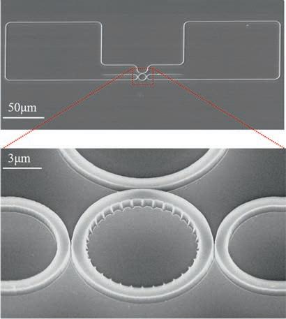
Scanning electron microscope images of the tunable vortex microlaser.
On an InGaAsP multiple quantum well platform, the microlaser consists of a main micro-ring cavity coupled to an external feedback loop that enables the on-demand chiral control by selective pumping and thus enforces the unidirectional coupling between the two circulating modes in the micro-ring.
The angular grating is patterned on the inner side wall of the micro-ring to produce the vortex laser emission of variable topological charges.
Inhalation Toxicology of Chlorine Gas On-a-Chip
Chlorine is one of the most commonly manufactured chemicals in the US, which is mostly used in industry and house cleaning products. Gaseous chlorine is poisonous and it has intermediate water solubility with the capability of causing acute damage to the upper and lower respiratory tract.
This project describes a major interdisciplinary research and development effort motivated by the significant and evolving threat posed by chlorine (Cl2).
The overarching goal of the project is to establish an entirely new approach to the development of biomarkers and effective medical countermeasures for Cl2-induced respiratory complications by transforming the conventional methods of modeling and predicting the toxicity of inhaled Cl2 gas in human lungs. To this end, the project uses the power of lung-on-a-chip technology to create bioengineered in vitro platforms that can reproduce the living tissues of the human respiratory tract and their native microenvironment, simulate realistic and physiologically relevant exposure conditions, and visualize and measure an array of biological responses to inhaled Cl2 gas for quantitative microfluorimetric and multi-omics analysis.
It represents a major undertaking that seeks to address the pressing unmet need for predictive and alternative technologies for inhalation toxicology of Cl2 by exploiting recent innovations made in the field of organs-on-a-chip. This work is led by postdoctoral fellows Sezin Aday Aydin and Pouria Fattahi; their supervisor Dr. Dan Huh of Penn’s Department of Bioengineering, and pulmonary immunologist Dr. Scott Worthen of the Children’s Hospital of Philadelphia, with funding from the Biomedical Advanced Research and Development Authority (BARDA).
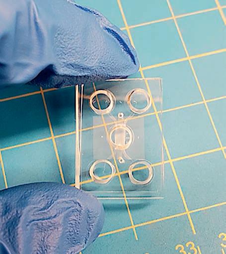
A photograph of the lung-on-a-chip.
Ferroelectric Nitride Materials for Nonvolatile Memory
The speed of computing systems operating on big data sets or implementing artificial intelligence (AI) algorithms has reached a bottleneck known as the “memory wall”, where the time and energy expended writing and reading data to and from memory far exceeds that consumed by the central processing unit (CPU).
Nonvolatile memory (NVM) is a type of memory that does not need to consume power to maintain its stored data. Embedding NVM in very close proximity to the CPU can greatly reduce the time and energy required to gather data for the processor and to store that data once the processor completes its calculations.
Of the competing NVM technologies, those based on ferroelectric materials are particularly promising for their low write/read energy and high access speed. Unfortunately, the most common and widely utilized ferroelectric materials require high temperature processes and contain elements that can spoil the performance of the transistors in the CPU, making them difficult to tightly integrate with the CPU. To address these challenges, Penn researchers are exploring a recently discovered ferroelectric material, Aluminum Scandium Nitride (AlScN), which can be deposited at low temperatures (≤ 350 °C) and whose constituent elements pose little risk to transistor performance.
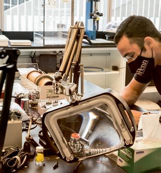
A major challenge with this new material is reducing the voltage required to write data to the memory to be compatible with modern CPUs, which required deep thickness scaling.
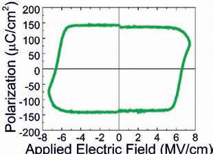
So far, Penn has demonstrated ferroelectricity in films as thin as 20 nm with corresponding write voltages of 13 V, switching speeds as fast as 200 ns, and 104 switching cycles. Current research is centered around growing thinner (< 10 nm) AlScN films with higher electric breakdown strength and lower coercive field.
This work was led by doctoral student Jeffrey Zheng, postdoctoral scholars Dr. Pariasadat Musavigharavi and Dr. Dixiong Wang, and faculty members Troy Olsson from Electrical and Systems Engineering and Eric Stach from Material Science and Engineering. The work is funded by the Semiconductor Research Corporation (SRC) and the Defense Advanced Research Projects Agency (DARPA) Tunable Ferroelectric Nitrides (TUFEN) program.
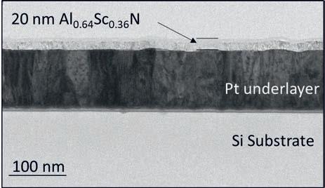
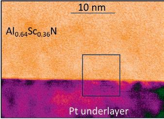
Bright field transmission electron microscope (TEM) image of AlScN grown on Pt. Top to bottom: Atomically resolved scanning transmission electron microscope (STEM) image of the AlScN/Pt interface. Ferroelectric hysteresis loop measured for a 20 nm thick AlScN material.
Fully Additive Fabrication of Electrically Anisotropic Multilayer Materials
Laminated multilayer structures comprising alternating layers of metals and insulators are useful in many applications such as capacitors, induction coils, magnetic cores, and sensors.
Structures consisting of these sequentially alternating layers can display interesting highly anisotropic material characteristics. In particular, micron-scale laminated cores that consist of electrical insulators and soft magnetic metallic alloys are regarded as a potential enabler of on-chip miniaturized magnetic devices such as transformers that will operate at high frequencies, handling watt-level power within small device volumes.
However, there haven’t been scalable and economical fabrication methods to make such anisotropic multilayer structures. Sequential, “top-down” physical vapor deposition of magnetic and insulating material can create laminated structures with controlled, nanoscale individual layer thicknesses. However, due to high built-in stress, it has poor scalability and vacuum-based deposition processes are costly. Typical electrodeposition-based lamination technologies are completed by subtractive processes.
After completing the multilayer electrodeposition, the sacrificial layers are selectively removed from the structure which is a complex process primarily due to the need for lithographically defined anchors to support suspended structure.
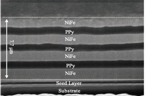
We propose a scalable and continuous fabrication (thus economical) process for building an anisotropic multilayer structure using the unique properties of the polypyrrole conductive polymer.
A laminated structure created using the developed process showed great promise for use in microfabricated inductor cores that operate at high frequencies, thus contributing to inductor volume reduction needed in MEMS power sources and sensing or actuation systems.
This research was performed by Michael Synodis of the MicroSensors MicroActuators group (MSMA), and Mark Allen of Electrical and Systems Engineering department, University of Pennsylvania, and in part by Enachip, Inc. (Disclaimer: PI Allen holds an equity position in Enachip).
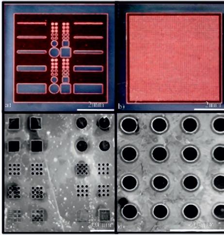
Left to right: An optical image of PPy-Sal electrodeposited through sample mold patterns of various geometries. An SEM Cross-sectional image of 3 sets of laminations with an added top layer of NiFe.
