27 minute read
National leadership
| High Performance Silica Optical Fibres
Advanced Beam Shaping in High Power Fibre Lasers
Challenge
Structured light, with spatially varying phase or polarization distributions, has given rise to many novel applications in fields ranging from optical communication to laser-based material processing. However, the efficient and flexible generation of such beams from a compact laser source at practical output powers still remains a great challenge. Here we describe an approach capable of addressing this need based on the coherent combination of multiple tailored Gaussian beams emitted from a multicore fibre (MCF) amplifier. We report a proof-of-concept structured light generation experiment, using a cladding-pumped 7-core MCF amplifier as an integrated parallel amplifier array and a spatial light modulator (SLM) to actively control the amplitude, polarisation and phase of the signal light input to each fibre core. We have demonstrated the successful generation of various structured light beams including high-order linearly polarized spatial fibre modes, cylindrical vector (CV) beams and helical phase front optical vortex (OV) beams.
Co-Investigator contact:
Professor Michalis Zervas mnz@soton.ac.uk
Progress
In our research, we have demonstrated experimentally the generation of various forms of complex beam (including azimuthally phase-chirped OV beams and radially/ azimuthally polarized CV beams defined on the higher-order Poincaré sphere) by coherent combination of individually amplified signals in a MCF amplifier (see Figure 1).
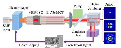
Figure 1: Schematic of the experimental setup. A single seed laser beam is adaptively shaped by a spatial light modulator (SLM) beam-shaper and the resultant field used to excite the individual cores of the MCF amplifier; multiple amplified beams are coherently combined to obtain various spatial modes in the far-field. | High Performance Silica Optical Fibres
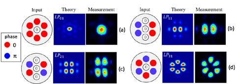
Figure 2: Scalar linearlypolarised (LP) mode generation. Idealised complex amplitudes of the individual cores required to generate specific LP fibre modes and the corresponding beam profiles in the far-field (in theory and measurement) Use of the MCF architecture provides for a highly integrated array of amplifiers and drastically reduces system complexity by enabling sharing of components across the multiple spatial channels, e.g. isolators, pump diodes and the SLM beam shaper that we used to control the amplitude, phase and polarization state of the signal light launched into each of the individual cores. Furthermore, since all the cores experience similar thermal and mechanical perturbations due to their very similar and close physical proximity, the environmental sensitivity of the relative phase and polarization between signals propagating through the different individual cores is substantially reduced compared to the case of arrays of physically separate single core fibre amplifiers. This leads to a corresponding reduction in active beam control requirements.
Scalar LP mode generation: We examined the generation of various higher order scalar linearly-polarised (LP) fibre modes by adjusting the input wavefront to the MCF amplifier. Here, we placed the relevant phase-plate of the desired LP mode in front of the LPO to construct the relevant correlation-filter. A few theoretical examples of the complex amplitudes for the individual beamlets required to generate specific LP modes are illustrated in Figure 2, along with theoretical and experimental far-field beam profiles. The experimentally measured far-field beam profiles agree very well with the corresponding theoretical predictions indicating that the complex amplitude of the individual beamlets is controlled as required.
Figure 2
Future Plans
This work paves the way to the generation of high power and reconfigurable structured light beams from simple and compact laser sources. The switching and high power structured light beams may offer advantages in a wide range of applications such as laser material processing, free-space optical communication and high-resolution imaging.
| Silicon Photonics
Integrated Silicon Photonic Circuits
Challenge
In the last 12 months we have focused on tackling two main research challenges: realisation of integrated near-IR circuits and systems (transceivers and LIDARs) and fabrication of wide band mid-IR photonic devices for spectrometers on chip.
Progress
We have developed a LIDAR with San Francisco start-up company, Pointcloud Inc. Fabrication is carried out at Southampton, using industry like processes, to trial and prototype devices and sub-systems. Following proof of principle, the company then incorporated the devices into systems that were fabricated in a commercial foundry. The work published in Nature (590, p256 (2021)), used a combination of foundry chips, a University of Southampton optical modulator, and company developed system software. The work demonstrated the most advanced integrated LIDAR system in the world to date, with accuracy of 3.1 mm at a range of 75 metres, using only 4 mW of light [1]. The system architecture is shown in Figure 1.
Co-Investigator contact:
Professor Goran Mashanovich g.mashanovich@ soton.ac.uk
Two important devices needed for spectrometers on chip have been demonstrated: wide band MMI splitter and broadband single mode waveguides. Both are based on subwavelength gratings and both show low losses. The waveguides were single mode from 2 to 4 μm and exhibited a propagation loss of 1.55 dB/cm across this range.
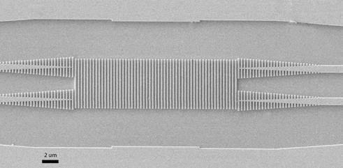
Operational range of the MMI splitter (see Figure 2) was 3.1 - 3.7 μm thus exhibiting a two-fold bandwidth enhancement over a conventional MMI around 3.4 μm, when considering imbalance and insertion loss (600 nm vs 300 nm). Importantly, this highperformance bandwidth was achieved using devices that have a small footprint and can be fabricated simply, with a single lithography and etch step, on a 500 nm-thick SOI platform [2]. | Silicon Photonics
Figure 1: LIDAR system architecture.
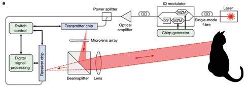
Figure 2: Wideband 2x2 MMI splitter.
Future plans
Future work will involve performance improvements of silicon near-IR and mid-IR devices and circuits, and will focus on: fabrication of more efficient optical modulators, integration of sources and room temperature mid-IR detectors, and realisation of spectrometers on chip.
References
[1] C. Rogers, A. Y. Piggott, D. J. Thomson, R. F. Wiser, I. E. Opris, S. A. Fortune, A. J. Compston, A. Gondarenko, F. Meng, X. Chen, G. T. Reed and R. Nicolaescu, “A universal 3D imaging sensor on a silicon photonics platform,” Nature, vol. 590, pp. 256–261, 2021, https://doi.org/10.1038/s41586-021-03259-y [2] C. Stirling, R. Halir, A. Sánchez-Postigo, Z. Qu, J. Reynolds, J. Penadés, G. Senthil Murugan, A. OrtegaMoñux, J. Wangüemert-Pérez, Í. Molina-Fernández, G. Mashanovich, and M. Nedeljkovic, “Broadband 2x2 multimode interference coupler for mid-infrared wavelengths,” Opt. Lett. 46, 5300-5303 (2021). https://doi.org/10.1364/OL.439985
AI-Assisted Nanofabrication
Co-Investigator contact:
Professor Kevin MacDonald kfm@orc.soton.ac.uk
Challenge
Focused ion beam (FIB) milling is a vitally important direct-write process for rapid prototyping and materials/device characterisation in both fundamental research and industrial manufacturing of nano-/microtechnologies. However, establishing process parameters for any specific task is a multi-dimensional optimisation challenge, typically undertaken by iterative (i.e. time-consuming and therefore costly) trial-anderror.
Progress
We have shown that deep learning – a neural network trained on the basis of prior manufacturing experience – can predict the outcome of FIB milling processes with high accuracy, taking account of instrumental and target-specific artefacts. Predictions are generated within a few milliseconds, so the methodology may be deployed in near real-time to expedite optimisation and improve reproducibility in FIB processing.
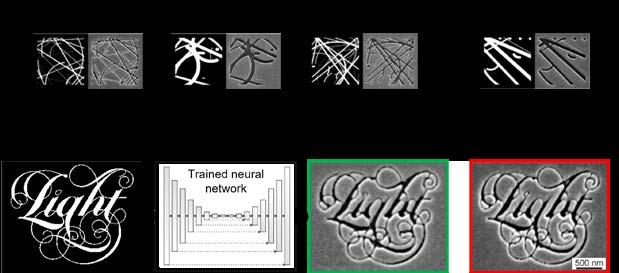
By way of demonstration, we consider the milling process for arbitrary 2D binary patterns etched into gold thin films, i.e. structures common to a range of nanophotonic/plasmonic applications, from metamaterial devices to spectroscopy (esp. surface-enhanced Raman) and seeded nano-materials growth. Simulations are performed by a conditional generative adversarial network trained on a set of binary designs and corresponding scanning electron microscope (SEM) images of samples fabricated with a range of FIB process parameters (see Figure 1a). The trained network is then able to accurately predict process outcomes for previously unseen designs - specifically their appearance in SEM imaging, as a strong gauge of process accuracy and quality (see Figure 1b).
This artificial intelligence-enabled capability can markedly reduce the number of experimental dose-test iterations required for (and therefore time and cost of) developing and optimising new FIB nanofabrication processes. The methodology may also be deployed for early fault (e.g. beam alignment, aperture damage) detection, and to maintain performance (i.e. consistency of outcomes from established processes) against ageing of the ion source and beam apertures. | Large-Scale Manufacturing of Metamaterials and 2D Materials
Figure 1a
Figure 1b
Figure 1: Deep learning simulation of FIB nanofabrication. (a) The neural network is trained on a set of randomly generated binary designs, SEM images of samples manufactured to those designs by FIB milling in a 50 nm thick gold film, and detail of the ion beam parameters used in their production. (b) The trained network predicts the outcome of FIB milling processes – the expected appearance of a sample in SEM imaging [outlined in green] – for previously unseen designs. For comparison, the actual outcome – an SEM image of a sample fabricated to the design on the left – is shown outlined in red on the right.
Future plans
Improvements in the predictive capabilities of the network may be achieved through optimisation of the training process and expansion of the training dataset, such as to encompass other substrate materials, different layer thicknesses and multilayers. There is considerable scope for functional enhancement of FIB/SEM systems, as integrated micro/nano-manufacturing and sample characterisation platforms, through the application of machine learning methodologies. It is also possible that neural networks trained for applications to FIB process development and control could contribute to new scientific understanding of the milling process (i.e. ion beam-target interactions).
References
O. Buchnev, J. A. Grant-Jacob, R. W. Eason, N. I. Zheludev, B. Mills, and K. F. MacDonald, “Deep LearningAssisted Focused Ion Beam Nanofabrication,” Nano Lett. (in press).
Manufacturing 2D Materials
Co-Investigator contact:
Professor Dan Hewak dh@orc.soton.ac.uk
Challenge
To achieve CMOS compatible, wafer scale processing of 2D materials for optoelectronics applications, demonstrating significant improvements in electrical and optical properties along with improvements in the manufacturing processes, in particular wafer scale deposition.
Progress
As we enter the final stages of our activities in the Future Photonics Hub, and following success in the demonstration of improvements in physical properties of 2D materials, efforts are now focused on advancing our manufacturing capabilities relevant to the commercial supply of these materials. Over the past years, we have developed a series of chemical (CVD) and physical (PVD) protocols for 2D film growth and in parallel with this, scaling these methods to 4-inch, 6-inch and now in 2022, 8-inch wafer dimensions. To evaluate and fully characterise our materials, in addition to our own device oriented experiments, samples are provided to a broad range of industrial and academic collaborators from which we obtain valuable feedback on their performance.
To enable 8-inch wafer scale depositions we have under construction a unique and bespoke deposition apparatus, in collaboration with local SME Themic Edge Ltd. We are now in the material testing and assembly process, and have tested five different refractory materials for the suitability within the deposition chamber, in particular, investigating the effects of H2S on equipment and components. This represents one challenge identified, that is the compatibility with the furnace hardware with high temperature in a corrosive atmosphere. A diagram of the apparatus under development is shown in Figure 1.
Figure 1: (a) Engineers rendering of final equipment with (b) Detail of atmosphere controlled furnace chamber. | Large-Scale Manufacturing of Metamaterials and 2D Materials
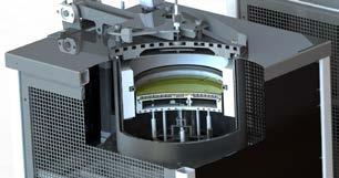

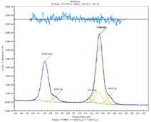
Figure 2: Optical microscope image of molecular beam epitaxy grown of antimonene with characterization by X-ray photoelectron spectroscopy (XPS) which provides both material (by element) and their chemical state shown in inset. Note the flaw (upper right of centre) is an intentional scratch to allow focussing of the image.
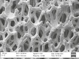
Figure 3: Scanning electron microscope image of a nickel nanofoam which has been conformally coated with graphene using our deposition protocol. These materials form an active part of next generation fuel cells. Work in progress with the University of Northumberland. A wide range of large-scale 2D materials, including graphene, hBN, TMDCs have been developed via CVD, Van der Waals epitaxy and ALD. Examples of materials shared in the past year include 2D MoO3 to the University of Glasgow and they convert it to MoTe2. Sheffield University produces antimonene and we characterise it, MoS2 and WS2 samples to the Singapore University of Design and Technology and graphene samples to the National University of Malaysia and Northumberland University. We have also expanded our network of internal collaborators with work on energy storage electrodes made of silicon nanowires and 2D MoS2 being undertaken with Electronics and Computer Science at the University of Southampton, fabricating large-area heterostructure samples. This material group has also sparked a new collaboration with Engineering at the University of Southampton on the testing of electrodes in lithium-ion batteries. Examples of these materials are illustrated in Figures 2 and 3.
Amongst our industrial collaborators, work with VTT Technical Research of Finland has expanded to include work on demonstrated ferroelectric field effect transistor memories. Ongoing activities supporting other research includes providing materials to three current EPSRC grants EPSRC EP/T014733/1, Fiberized Platforms for Integrated Nanosheet Materials, EPSRC EP/V040030/1, 3D Nanophotonics in Artificially Structured Chalcogenide Materials and EP/S036369/1, Composite material hollow core fibres for active photonics.
Future Plans
We continue to work towards our final objectives, bringing together our ongoing work developing new chemistry routes to 2D material synthesis and combining these with practical methods of depositing the materials at wafer scale using deposition protocols at wafer scales and compatible with modern semiconductor processes. This includes the completion of the fabrication of an 8-inch (200 mm) capability for wafer scale processing up to 1200oC under inert or reactive gas conditions. This, combined with the improvements in deposition protocols will be a major step forward in bringing wider spread commercialisation of 2D materials.
References
Huang, Z-W., Hong, Y-H., Du, Y-J., Kuo, T-J., Huang, K. C-C., Kao, T. S. & Ahn, H., “Terahertz analysis of CH3NH3PbI3 perovskites associated with graphene and silver nanowire electrodes” in ACS Applied Materials & Interfaces, 24 Feb 2021, 13, 7, p. 9224-9231. Chen, J., Guo, S., Lin, D., Nie, Z., Huang, K. C-C., Hu, K., Ma, L., Zhang, F., Zhao, W. & Zhang, W., “Ultrafast nonequilibrium dynamic process of separate electron and hole during exciton formation in few-layer tungsten disulphide” in Physical Chemistry Chemical Physics, 4 Mar 2021, 23, 12, p. 7135-7144.
Directional VCSELs and Diffractive Optics for 3D Machine Vision
Challenge
3D vision and face recognition systems are now common in smartphones, but they utilise complex bulk optical systems that are very difficult and costly to assemble. Over the last two years we have been working in conjunction with IQE plc (key supplier of laser epitaxy to Apple and Huawei) on development of more compact replacement components for 3D face recognition systems for deployment in next generation smartphones. This project exploits our granted Photonic Quasi-Crystal patent portfolio which was recently purchased by IQE.
One of the key sub-modules is the infrared illuminator. This incorporates an array of very high power VCSELS, along with a diffuser component to provide a specific illumination pattern.
Co-Investigator contact:
Professor Martin Charlton mdc1@soton.ac.uk
VCSELs currently suffer from unavoidably large beam divergence angle (typically 600) requiring complex corrective optics, making the illuminator module bulky and expensive to assemble. They also require a complicated oxidation process that defines the laser aperture, and limits the power output.
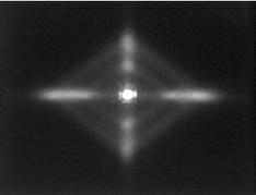
Our Photonic Crystal VCSEL technology solves the VCSEL beam divergence and power limitation problems, allowing control of the beam divergence angle direct from the chip dye without the need for external lenses (see Figure 1a). It also allows very large circular MESAs to be used, making them suitable for very high power LIDAR illumination, and high speed telecoms applications.z
Diffuser components are currently based on arrays of stalactite shaped glass microlenses, typically 30 μm in length, each with a unique length and curvature. These are incredibly difficult to manufacture making the diffuser one of the most expensive sub-components.
Utilising our legacy patents we have devised a completely novel technological solution for the diffuser component, replacing the long glass stalactites with a sub-micron thick nano-patterned silicon layer. | Large-Scale Manufacturing of Metamaterials and 2D Materials
Figure 1: (a) photograph of laser beam projected onto a screen. PQC device has far smaller laser spot due to reduced beam angle.
(b) schematic cross- section of PQC VCSEL illustrating beam shaping concept. Figure 1a
Laser beam projected onto screen
Standard VCSEL
QPC VCSEL – much smaller spot Figure 1b
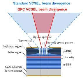
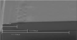
Figure 2: FIB/SEM cross section of the VCSEL showing the oxidised layers. Central inset shows the full device, and where the cross section images were. Circular device
Cross-section
Epitaxial mirror layersa
Lateral oxidation distance
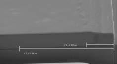
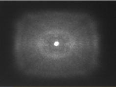
Figure 3: Example diffuser beam patterns projected onto a screen.
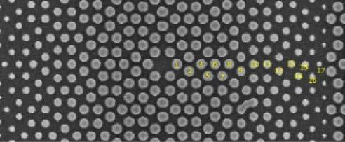
Figure 4: SEM image of nm scale pattern created by e-beam lithography. | Large-Scale Manufacturing of Metamaterials and 2D Materials
Progress
First sets of PQC-VCSEL devices demonstrated greatly reduced beam divergence (figure 1b) and excellent electrical characteristics despite having very shallow holes and no aperture oxidation process step. Over the last year the fabrication process has been scaled up to full 6” wafer process, and a 6” wafer-level aperture oxidation process developed to commercial standard (fig 2). Next gen devices incorporating the new process and deeper holes are expected to demonstrate extreme beam shaping, and high power illumination.
PQC-diffuser component required development of a reliable end-to-end manufacture process from scratch. Over the last year several new designs have been fabricated and tested, increasing optical efficiency to >96% and achieving the required diffusion pattern (figure 3), and specifications as required for current mobile phone systems. The key challenge was speeding up the electron beam lithography process used to define the complex nm scale pattern on glass to allow full 6” wafer patterning (figure 4)
Working closely with IQEs manufacturing teams in Taiwan we are now in the process of scaling up to mass-manufacture using cutting edge ‘nano-imprint’ lithography process and will commence production of ‘customer demonstrator’ devices. A technology licencing agreement is currently under negotiation, and IQE plan to release a product based on the PQC-diffuser technology within the next 12 months.
| Integration
Development of Integrated Mid-Infrared Photonic Devices and Systems
Co-Investigator contact:
Professor Jon Heffernan jon.heffernan@ sheffield.ac.uk
Challenge
To demonstrate the integration of semiconductor devices such as lasers, LEDs and detectors on single chips for functional manipulation of mid-infrared light.
Progress
Our research in this platform is aimed at developing new manufacturing methods that will allow the integration of a range of photonics components, such as lasers, LEDs, detectors and quantum devices with passive semiconductor components such as waveguides, modulators and interferometers on GaAs, InP, silicon or silicon/Ge platforms. The overall aim is to demonstrate new forms of integrated smart photonics chips such as integrated sensors, spectrometers, quantum processors and lab-on-chip diagnostic tools. The heterogeneous integration of different materials, devices and process that in the past were often considered incompatible is now a major focus of the global development of smart electronic systems. But there remain many challenges in developing the manufacturing methods.
In this theme we have been continuing the development of two technological approaches to creating integrated photonic systems; with a focus towards on-chip integrated sensors with mid-infrared photonics. The University of Southampton has worked closely with the epitaxy and device teams in Sheffield to develop and evaluate new approaches to the problem and has been working with industry and selected other academic groups to further the field.
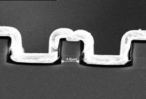
The development of integrated quantum cascade lasers (QCLs) on Si/Ge waveguide platforms has continued and further iteration of the complex processing steps to make the III-V materials compatible with Si/Ge process has been the focus in the last year. Improved waveguide designs have been fabricated by electron beam lithography (see Figure 1c) and several critical process improvements have been made that were sources of poor heat management of the integrated lasers. A final, fully optimised fabrication run will be completed in early 2022 and initial demonstration of sensing functionality will be addressed. | Integration
Figure 1a Figure 1b Figure 1c
Figure 1: (a) Observation of Rabi oscillations in the spectra of a CW operating quantum cascade laser (QCL) at 5.75microns (b) indicating the presence of non-linear effects. These lasers will be integrated on Si/Ge waveguides (c) and open the possibility for integrated frequency combs. In addition, improvements to the QCLs themselves have been made and high efficiency lasers operating CW have now been demonstrated, providing excellent optical coupling to waveguides. In addition, we have found the quality of these lasers has led to the observation of Rabi-splitting (see Figure 1a) in the spectra of the lasers operated under CW condition. This demonstrates non-linear optical processes in the laser and is a route towards high resolution sensors on frequency combs. On-chip frequency combs will be a major step forward in mid-IR integrated sensors.

We are also pursuing a second approach to integrated mid-IR sensors by developing homo-epitaxial integration of active components with waveguides. In particular, we are developing a platform based on mid-IR waveguides fabricated on GaAs and InP. Here the challenge is to develop buried GaAs waveguides with dimensions of 5-10 microns, which places challenges on the epitaxial process itself. We continue to develop this approach seeking to reduce defects associated with these thick layers and also improve conformal epitaxy processes over GaAs waveguides. These improvements to the epitaxy process will lead to a reduction of the relatively high losses previously measured by us in early fabrication runs. Wafer uniformity is also being investigated to evaluate manufacturing tolerances for this approach.
Figure 2: Atomic Force Microscope (AFM) image of Indium droplets in nanometre-sized etched pits on an InP substrate. Indium is deposited on the pre-fabricated wafer and diffuses to the etched pits to form droplets. The droplets are subsequently exposed to Arsenic and converted to InAs quantum dots. The technique is a new approach to the deterministic positioning (site-control) of quantum dots. Other research strands in this Integration theme include the development of a novel approach to site-control of quantum dots in InP (see Figure 2) in which indium droplets are first of all site-controlled followed by their conversion to quantum dots. We have also been developing a novel 2D material based on antimony. Antimonene is expect to have useful optical properties for sensing and we have been developing the integration of this material grown by MBE with GaAs–based devices. At this time, initial growth of antimonene by this method has been inconclusive, but further epitaxial optimisation is planned.
| Integration
Novel Forms of Interconnection and Device Integration for Emerging Multimode, Multicore, Hollow-Core and Multi-Component Optical Fibres

Challenge
To develop novel means of interconnecting emerging new fibre types under development within the Future Photonics Manufacturing Hub to other fibres and/or to other functional components.
Progress
Our research has focused on the development of new fibre optic components, interconnection devices, and characterisation of multi-component soft glass optical fibres.
Firstly, we have investigated the issue of optical interconnection between verticalcavity surface-emitting lasers (VCSELs) and hollow-core fibres (HCFs). Note that direct HCF interconnection to a laser diode or photodiode (i.e. without any short piece of interconnecting solid core fibre) is a very important requirement in order to fully utilise the unique characteristics of HCFs. Many different platforms have been investigated previously in the development of solid core fibre coupled optical devices. During the past year we have focused on two particular HCF interconnection approaches, i.e. direct butt coupling and simple two-lens imaging, for coupling to a VCSEL operating at 850 nm. We observed that butt coupling provides only poor coupling efficiency (~10%) due to the poor mode field diameter mismatch but that a two-lens system can be used to achieve very high coupling efficiency (~96%) with excellent output beam quality. A prototype packaged device was successfully fabricated in-house and in the next period we plan to further explore other semiconductor laser to HCF coupling challenges at other wavelength bands - with particular interest in the interconnection of mid-IR quantum cascade lasers and visible/UV laser diodes to HCFs.
Secondly, using compact micro-optic collimator technology, we have further developed various inline fibre components based on specialty optical fibres. In particular, we have focused on high-power fibre optic components and successfully managed to develop several industrial grade devices (e.g. few mode fibre isolators) operating at >1W with good stability at 1550 nm and supplied these to a commercial partner. In addition, we
Co-Investigator contact:
Professor David Richardson, djr@orc.soton.ac.uk | Integration
Figure 1a Figure 1b
Figure 1: (a) Direct HCF interconnection to a VCSEL and, (b) 3D printed mode scrambler. have continued our collaboration with NTT in Japan on high spatial density multicore fibre amplifiers (i.e. 6-mode 7-core fibre amplifiers) for ultrahigh spatial density long haul transmission.
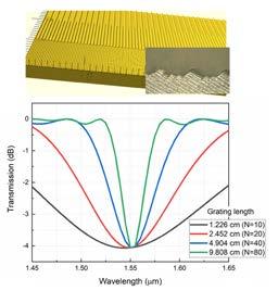
We have also worked on low-loss and broadband mode scramblers for mode division multiplexed transmission based on few mode fibres. By simply shortening the length of the long-period fibre grating (LPG), the optical bandwidth can be significantly enhanced. For example, >230 nm bandwidth is predicted in our simulations with a grating length of 0.613 cm. In an experimental demonstration we fabricated a mechanically induced LPG using a commercially available 3-dimensional (3D) printing technique. Wideband operation was confirmed over the C band and a low loss (0.2 dB) and low mode dependent loss (0.1 dB) were achieved.
In addition, we have worked on the characterisation of multi-component soft glass fibres for rare earth doped fibre amplifiers/lasers. In general, soft glasses have poorer glass stability than silica glasses, with low glass transition temperatures and low tensile strengths. Special attention needs to be applied in handling these fibres. Working with the Zepler Institute soft glass fabrication team, we are looking to develop wideband amplifiers using germanotellurite (Ge-Te) glasses which promise broadband emission and improved chemical/mechanical glass stability. In this platform we are working to develop splicing techniques to these fibres and to understand the spectroscopic characteristics of erbium incorporated at high concentrations into the core. Our first target is to develop a compact, seamless C+L band amplifier and our preliminary fibre characterisation results look encouraging in terms of emission and absorption bandwidths. We are also exploring ways to extend the operating bandwidth of silica fibres using multistage designs and optimised inline filtering.
Future Plans
We will continue to focus on the integration aspects of all the emerging fibre types referred to above with a focus on loss reduction, extended wavelength coverage and increasing the range of device functionalities possible.
| Light Generation and Delivery
Progress on Wideband Optical Amplifiers
Challenge
To exploit the advantages of compound ’soft’ glasses for the development of ultrabroadband optical amplifiers. By widening the amplification bandwidth available to optical communications, we aim to enable a significant increase in transmitted data traffic through the existing optical network infrastructure.
Progress
This year we have focused our activities to the development of optical fibre amplifiers based on non-silica glass hosts. The idea is to exploit the excellent thermo-mechanical properties of glasses developed so far in the hub to produce optical amplifiers with considerably broader amplification bandwidth than the standard ones that use silica as the host material. If this research is successful, these novel fibre amplifiers will be able to support optical communication links with far increased data capacities.
Co-Investigator contact:
Professor Francesco Poletti frap@orc.soton.ac.uk
It is well established in the literature that a linear proportionality exists between the refractive index of a rare earth doped glass host and its luminescence bandwidth. ‘Soft’ glasses with a higher refractive index than silica, however, are normally considerably more difficult to draw into useable fibres due to worse mechanical properties and a much higher tendency to crystallisation than silica. Here we exploit the progress made in this project in the previous years in developing robust and crystallisation-free high refractive index glasses. Amongst the various glass host compositions and dopants that we have studied this year, we focus in this report on germanate-tellurite (Ge-Te) glasses doped with erbium, aiming to produce a wideband amplifier cantered around in the C-band of optical communications.
The newly developed Ge-Te glass composition was produced in an ultra-dry glove box furnace, which allows both a dry atmosphere and very low contamination. With an absorption coefficient of <5 dB/m at 3 μm where water absorption peaks, this glass is, to the best of our knowledge, the driest novel soft glass yet developed. Lowering the OH- content in the glass improves its overall spectroscopic characteristics. As can be seen in Figure 1a, the luminescence bandwidth of such a preliminary prototype softglass fibre is very promising, and considerably wider than that of silica. Next, we have optimised the erbium concentration on this type of glass and found that an optimal | Light Generation and Delivery
Figure 1a Figure 1b
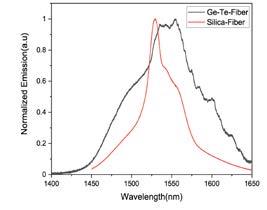
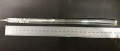
Figure 1: (a) comparison between the Erbium emission spectrum of the newly developed Germanate-Tellurite fibre and that of a conventional silica fibre.
(b) Fibre fabrication process: from bulk glass billets (cladding: transparent and Er:doped core: pink) to extruded preform and drawn fibre. existed around 4 mol% (1.76X10²¹ ion/cm3). This concentration was used to prepare the glass for the fibre core. The cladding glass was erbium free, and its composition tailored to provide a refractive index difference that would allow a single mode fibre operation and compatible thermo-mechanical properties with the core glass for fibre drawing (see Figure 1b). Finally, we have recently produced an Er-doped germanate-tellurite fibre from such glasses. Its emission at wavelengths around 1.5 um was measured and it is was found to be twice as large as that of a commercial silica doped fibre. Additional spectroscopic measurements are currently ongoing but these results are already quite promising.
Future Plans
In the near future, we plan to incorporate the newly developed ultra-broadband fibre into an optical amplifier, and to measure its full dynamic performance. Beyond this, we plan to study the incorporation into this very promising host glass of other rare earth elements (Tm3+, Pr3+), as well as of multi active-ion co-dopant schemes such us Er3+/ Tm3+, Er3+/Pr3+ and Er3+/Tm3+/Pr3+. We also plan to study the performance of other ‘soft’ glasses with even higher refractive index, aiming to develop a suite of efficient optical amplifiers covering the full spectral range 1260 – 1675 nm.
| The team
Deputy Director and Manager: Professor Gilberto Brambilla, University of Southampton Co-Investigator: Professor Martin Charlton, University of Southampton Project Administrator: Liz Gilbride, University of Southampton Deputy Director: Professor Jon Heffernan, University of Sheffield
Public Engagement Leader: Pearl John, University of Southampton Business Development Manager: Amir Kayani, University of Southampton Industrial Liaison Manager: Dr John Lincoln Co-Investigator: Professor Goran Mashanovich, University of Southampton
Principle Investigator and Director: Professor Sir David Payne, University of Southampton Co-Investigator: Professor Francesco Poletti, University of Southampton Co-Investigator: Professor Graham Reed, University of Southampton
Co-Investigator: Dr Natalie Wheeler, University of Southampton Co-Investigator: Professor David Richardson, University of Southampton
Co-Investigator: Professor Michalis Zervas, University of Southampton Co-Investigator: Professor Dan Hewak, University of Southampton
Research and Relationship PR Officer: Michelle Mitchell, University of Southampton
Co-Investigator: Professor Jayanta Sahu, University of Southampton
Co-Investigator: Professor Nikolay Zheludev, University of Southampton
With special thanks to:
Carbon Trust, Huawei, Honeywell Aerospace, II-VI Photonics, IQE, IS Instruments, Lightpoint Medical, Lumenisity, Merck, Microsoft, NorthLab Photonics, Northrop Grumman, Oclaro, Phoenix Photonics, PragmatIC Printing, QinetiQ, Rockley Photonics, Seagate Ireland, Sestosensor, SPI Lasers, Breakthrough Prize, Defence Science and Technology Laboratory (DSTL), European Office of Aerospace Research & Development, Engineering and Physical Sciences Research Council (EPSRC), European Commission, Horizon 2020, Innovate UK, Royal Academy of Engineering, Royal Society


