
increasing bandwidth: increasing the thickness of the substrate [22], using stub [23], negative capacitor/inductor [24], Non-Foster Matching Circuit [25], and defected ground structures [26], magneto-dielectric substrates [27], electromagnetic band-gap (EBG) structures [28], and metamaterial resonators [29], using fractal geometries [30], and cavity backing [31]. The ever-increasing demand for wireless applications that deliver high-quality content to a large number of users simultaneously has resulted in a massive increase in data volume, which has resulted in a spectrum shortage in the microwave band, causing networks to become congested. To address this issue , researchers have moved to millimeter wave (30 GHz–300 GHz) usage, where we find some appealing applications, for example, allocated around 60 GHz wireless digital data transfer between a highdefinition TV (HDTV) and a DVD player of uncompressed high-definition video, autonomous robots and back hauling allocated around 80GHz; and motion sensing at 100GHz. The mm-wave choice is appropriate for the main reason that mmwave systems have larger available bandwidth as compared to other communication frequencies below 10 GHz because of a metric called fractional bandwidth (for example, designing a system that occupies 5% of the operating frequency means having 5 GHz of available bandwidth at 100 GHz) and it is well-known that the larger bandwidth enhances the channel capacity. The losses caused by electromagnetic wave atmospheric absorption at higher frequencies remain constraints for millimeter wave applications. Therefore, antenna arrays come as a solution to accomplish higher gain andefficiency.Forgainimprovement,antennaarraysareused in [32
34]. This work aims to demonstrate the effect of array configuration on antenna performance.
2. THE PROPOSED APPROACH
To understand how an antenna works, it's necessary to look at its physical components, the characteristics and parameters that describe its behavior, and the model that must be used to evaluate it. Here's a quick survey on microstrip antennas: It can take numerous shapes, including dipole, square, triangle, circular, rectangular, and other more intricate configurations, but rectangular and circular are the most widely utilized since they are easy to analyze and build. A printed antenna is activated by a feed line, which implies that energy is delivered to the patch so that we can directly affect and adjust its radiation to achieve high performance. The substrate serves as a dielectric substance on which the circuits are etched, and the structure is supported by a mechanical portion. Lowdielectric-loss substrates are widely utilized to increase antenna performance, and low-relative-permittivity substrates are regularly used to improve radiation while lowering losses. Ceramics, ferromagnetic materials, semiconductors, and synthetic materials are among the materials utilized as substrates. Patch geometry, excitation technique, substrate thickness, and dielectric constant are the primary determinants of antenna characteristics or parameters, which include reflection coefficient, directivity,
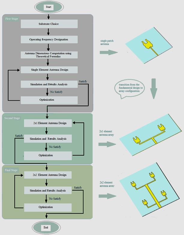
gain, bandwidth, efficiency, and quality factors. A plan has been drawn to produce an antenna with the desired features of high gain and wide bandwidth. Figure 1 depicts the modeling process. The plan specifies the steps that must be taken to achieve the desired antenna. These steps represent three distinct stages that show how array configuration can be used to boost gain. The first stage begins with the selection of the substrate material, which is critical in the search for a highfrequency antenna that is both efficient and effective. It's worth noting that we started with a square patch antenna and then modified the shape to improve the antenna's attributes, such as bandwidth and gain. The patch's dimensions are determined using the well-known theoretical formulas (1) to (5) as given below. The best results from the first stage are usedtocalculatethe finalresultsforthe secondstage,andthus the proposed 2×2 array antenna in the third stage. Following the completion of the needed findings, we must construct the antenna based on these findings; the design that emerges is the proposed antenna. The work is based on CST software computing and design.
2.1 Modelling Equations
Patch size calculation process: - calculation of the width:
c: Velocity of light in air.
fr: operating frequency.
εr: dielectric permittivity.
- Calculation of length:
Effective dielectric constant of the substrate:
h: Height of the substrate
Effective length:
Leff = C 2fr√∈reff (3)
Length extension:
∆L= 0412h (w h+0264)(∈reff+03) (∈reff 0258)(w h +08) (4)
L= Leff − (2 ∆L) (5)
The calculation procedure above is done using the transmission line model analysis.
3. DISCUSSION AND RESULTS
3.1 Antenna with a Single Patch
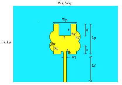
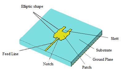
According to Figure 1 and as clarified in Figure 2, the proposed antenna design process in this work is initiated with a basic conventional design, consisting of a slotted rectangular-shaped patch with symmetric identical halfellipses located at the lateral edges; these elliptic shapes are the most sensitive parts of the antenna that directly
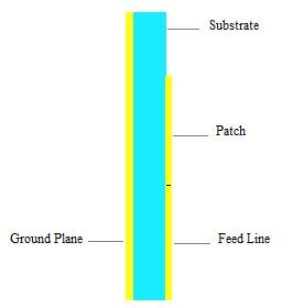
affect radiation characteristics, we will discuss in the results section. The copper representing the feed line and the patch isetched on the upper surface of a Rogers RT 5880 substrate (Figure 3 a), with a thickness, relative permittivity, and loss tang of 0.8 mm, 2.2, and 0.0009, respectively, while the ground plane is etched beneath the substrate (Figure 3 b), with a copper thickness of 0.035 mm. The patch contains small vertical stubs in the advanced part that appear to be a concavity; the lateral edges are semi-elliptic in shape, and they play an important part in the antenna's performance. To ensure impedance matching between the antenna and the feed line, a 50-ohm inset feed line approach is used. Because the antenna must be optimized to meet the desired performance characteristics represented in gain, bandwidth, and frequency of resonance, the lateral edges and the feed line width were then adjusted to be (Lp = 2.2 mm, Wp = 1.1 mm). The dimension results are detailed in Table
1. The use of the inset-feeding approach at the feed line's center point, as shown above, seeks to provide maximum impedance matching between the strip-line feed and the patch. The breadth of the feed line, like the elliptical-shaped horizontal radius, has a significant influence on antenna behavior. The patch was split in front, generating a hollow that resembled a double vertical little stub, while the ground structure was left undamaged on the other side. (CST) software is used to optimize the size and dimensions that result.
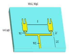
3.2 2×1 Array Antenna
We expanded the array arrangement to two patches, as shown in Figure 4, to demonstrate the gain enhancement and since the array technique improves the antenna's behavior. Note that throughout the design process, except for the feed lines, we must maintain the previous results unaltered. After improving the radiating properties, the resulting antenna was determined to have a dimension of 15.8×7 mm2. Table 2 describes the geometry of the obtained 2x1 array antenna model. S in Figure 4 denotes an inter-element spacing that has a significant impact on outcomes, and it was chosen for greater isolation between individual elements (patches).
3.3 2×2 Array Antenna
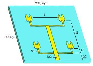
The same approach is used in this design to obtain higher gain values and improve antenna performance. The previous stage's resultant antenna design is used as a fundamental element to build a 2×2 array antenna. This work's intended antenna is shown in Figure 5. Four patches are employed, each of which is fed by a corporate feeding network. The secondary direct feed line diameter was adjusted to ensure antenna impedance matching. As a result, the resultant antenna was able to achieve a promisinglytiny size (18 × 16.1 mm2). The horizontal and vertical spacing lengths between elements are 6.74 mm and 9 mm, respectively, for S and S1. The dimension findings for the 2×2 array antenna are listed in Table 3.
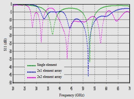
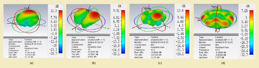
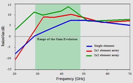
The performance of every antenna is continually evaluated by monitoring the following parameters: return loss, gain, radiation efficiency, and impedance bandwidth. The data collected from the earliest to the last stages describe the performance of the antenna throughout the optimization process. The suggested antenna has more operational frequency bands than the first and second-stage antennas; in fact, multiband behavior implies more users and applications. The operating frequency ranges of the proposed antennas, as illustrated in Figure 6, range from 27 to 58 GHz and include various frequency bands such as V, Q, and Ka, whereas the single patch and 2×1 array antennas start at 36 GHz and 43 GHz, respectively. We know that the reflection coefficient depends on the value of S11 and should be less than -10 dB in magnitude; Figure 6 depicts the return loss comparison obtained across the three stages, revealing that the 2×2 array antenna of interest has a return loss of -34.8 dB at 43.2 GHz with an ultra-wide bandwidth of 12.2 GHz and a return loss of -14.8 dB, -24.33 dB, and -25 dB at 28.3 GHz, 32 GHz, and 57.5 GHz, respectively. Asa consequence, it'sevidentthatthe gain might be enhanced if there were more patches. Figure 10 demonstrates the gain improvement from a single patch to a 2×2 array antenna. Based on the basic resonance frequencies of the three stages, we deduce that the frequency area where the antenna performs efficiently converges towards 43 GHz, which explains why the observed gain has reached 13.8 dB with 92 percent radiation efficiency at the resonance frequency of 43.2 GHz.
By comparing the three stages according to Figure 6, we aimed to maximize the gain and efficiency as much as possible even if the improvement is a little weaker than expected. Figure 10 depicts the curve produced by the variation of gain as a function of frequency. The finalized design of the proposed antenna is deemed to have promising operating characteristics.
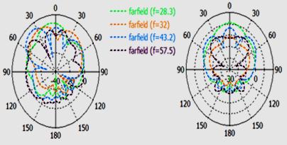
Radiation is so important in determining most of the characteristics, including beam width, beam shape, and directivity. The polar pattern plots at various spot frequencies for the antenna during the design stages are depicted in Figure 7. From the corresponding results (Table 5) of these figures, we conclude that the antenna keeps nearly stable directional radiation in E-plane or H-plane during the different design stages, and it achieves a high directivity at the frequency of 43.2 GHz, represented by the lowest Half Power Beam-width (HPBW) of 25.5° in E-plane. To achieve satisfactory results, primary antenna radiation characteristics have been researched and improved. These findings are revealed in table 5. If we look at each frequency band separately, we can see in Table 5 that the more patches we add to the antenna, the more directional it gets, which means a narrower HPBW and lower side lobe level (SLL). As an example, we can observe that the final 2x2 array antenna design gives us excellent radiation
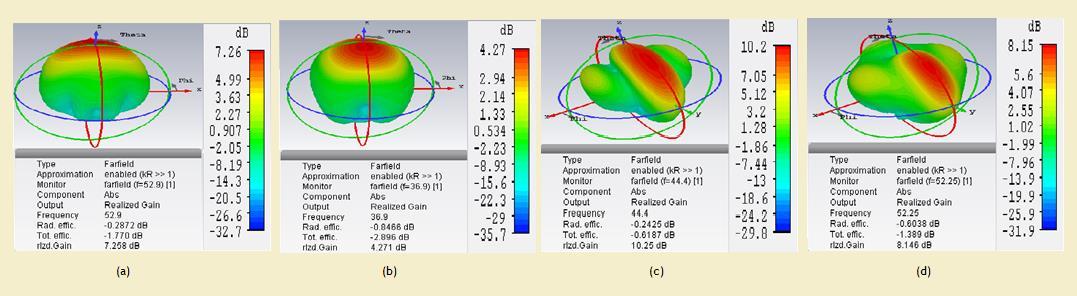
characteristics as compared to a single and 2x1 array antenna near the operating frequency of 43.2 GHz, in terms of numbers, 25.5 ° against 72.8 ° for HPBW and -7.5 dB against -15.8 dB for SLL. In addition to what was said regarding HPBW and SLL, and as we are focused on the evolution of gainandefficiency, thesame thingisnoticed for3Dradiation, representing the realized gain in Figures 8 and 9, where the gain at a given operating frequency rises from stage to stage at this operating frequency. Figure 10 confirms this concept, especially around 43.2 GHz in a range of about 17 GHz. At this point, the gain achieved was 13.8 dB with 92% of radiation efficiency. All of this adds up to the array configuration's contribution to the optimization of radiation properties, notably gain. The array arrangement of patches provides a significant boost in the realized gain of more than 3 dB, as well as efficiency and directivity. Imagine increasing the number of patches by the array configuration (2x2 and 4x4…), what will become the realized gain?
In addition to bandwidth, antenna gain is a key statistic for determining how well an antenna transmits and receives radio frequency (RF) signals. As shown in Figure 10, the proposed four-element array performs better in terms of gain, as evidenced by the fact that average and peak gains increase as the number of patch elements increases.
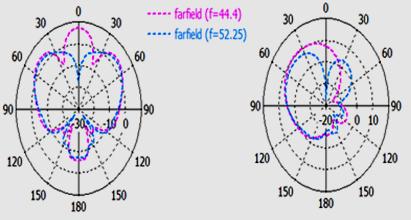
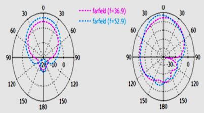
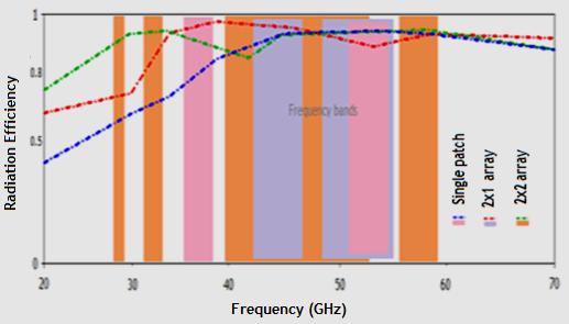
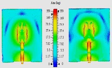
To follow the evolution of the efficiency during the different stages, we refer to Figure 11, precisely the operating frequency bands belonging to the resonance frequencies of 28.3 GHz, 32 GHz, and 57.5 GHz, and when compared to the other two antennas (single and 2x1 array), we notice that the proposed 2x2 array antenna has the highest value over the whole bands, except for the band corresponding to the resonance frequency of 43.2 GHz, where the proposed antenna is more efficient over a part of the band interval frequency (46.5 to 52 GHz), whereas the 2×1 array antenna is more efficient over the rest of the band. The increase in gain and bandwidth was mostly attributable to the optimal value of several design factors. As pointed out in the design section regarding the responsible part that significantly effects radiation characteristics, including gain and efficiency, now and in this context, it is necessary to explore the impacts of important design factors on the resonance performance of the proposed antenna. Figure 12 provides a more illustrated understanding of the purpose behind the usage of stubs, concavity,elliptic-shapedsides,and notches. Figure12shows that the elliptic-shaped lateral edges on both sides of the patch are the primary players in antenna performance or radiating power. As can be observed, current flows are more dominant andconcentratednearthestatedspots.Inadditiontothe major role of the elliptic-shaped lateral edges in radiating at 36.9 GHz, as shown in Figure 12 a, the stubs in the front at 52.9 GHz in Figure 12 b, also contribute to radiating, but with a little less where their role seems minor. The reverse is true for thecaseofnotches;thisistranslatedbytheamountsofcurrent present on the surface of the patch described in Figure 12 a, b. The notches and concavity are important in the proposed antenna's multiband behavior as they perturb the current distribution on the patch and change the coupling between the patchand the ground plane; theyalso create additional current paths that change the direction of surface current flows along the radiating patch towards the vertical stubs and elliptical laterals. To evaluate the performance of the suggested 2×2 array antenna, we have compared it to some recent works encompassing various frequency bands. This comparison is summarized in Table 4. In comparison to other antennas, our antenna has greater performance in terms of bandwidth, realized gain, and miniaturized size, in addition to its tiny and convenientfabrication.Ifgiventheopportunity,the suggested antenna may entirely cover the whole-mentioned 5G applications spectrum (27–60GHz), making it appropriate for a variety of applications needing high gain and large bandwidth.
4. CONCLUSION
A high-gain, efficient, and low-profile 2×2 patch array antenna has been suggested during this work for millimeterwave applications operating at 28.3GHz, 32GHz, 43.2GHz, and 57.5GHz. The antenna was designed and improved by using a CST (Conception Simulation Technology) simulator. because of its superior performance in terms of gain, 13.8 dB (more than 12 dB across nearly half of the bandwidth, preciselybetween40.5 and 45.5 GHz);efficiency, 92 percent; bandwidth, 12.2 GHz; small size, 1816.1 mm2; and narrower beamwidth,20.3°at43.2GHzThe2x2elementarrayantenna responds to the required millimeter-waves applications features, including 5G. So, it can be considered a positive choice. The coming task is to upgrade it to a 4×4 and 8×8 array antenna, by which we expect that we will further improve the efficiency and gain.
REFERENCES
[1] K. Carver, J. Mink "Micro-strip Antenna Technology", IEEE Transactions on Antenna and Propagation, vol. 8, no. 29, pp. 2- 24, Jan 1981, doi: 10.1109/TAP.1981.1142523
[2] A. Al-Ahmad, Y. S. H. Khraisat "Bandwidth Enhancement of Microstrip Patch Antenna," applied physics research, vol.11, no. 1, pp. 35-40, Jan 2019, doi:10.5539/apr.v11n1p35
[3] Y. Yashchyshyn, D.Vynnyk, V. Haiduchok, I. Solskii, Wu, C. Bogdan, G. and J. Modelski, “A Tunable and Electrically Small Antenna for Compact GNSS Receivers”, Remote Sensing vol. 13, pp 485. Jan 2021, &https://doi.org/10.3390/rs13030485.
[4] M. Fallahpour, R. Zoughi," Antenna Miniaturization Techniques: A review of Topology and Material-Based Methods,” IEEE Antennas and Propagation Magazine, vol. 60, no. 1, pp. 38-50, Feb 2018, doi: 10.1109/MAP.2017.2774138
[5] Y. Cao, K. S. Chin, W. Che, W. Yang, and E. S. Li, "A compact 38 GHz multi beam antenna array with multi folded butler matrix for 5 G applications," IEEE Antennas Wireless Propagation Letters, vol. 16, pp. 2996–2999, sept 2017.
[6] K. K. Sharma, R.K. Goyal, "Slotted Micro strip Patch Antenna at 60 GHz for point-to-point Communication," IEEE Explorer, pp. 371- 373, July 2016, doi: 10.1109/ICCN.2015.71
[7] G. V. Raviteja, "A 2x2 Millimeter-Wave Micro-strip Antenna array for 5G Applications”, European Journal ofEngineering Research and Science, vol. 4, no. 10, pp. 55-58, Oct 2019, doi: http://dx.doi.org/10.24018/ejers.2019.4.10.1581.
[8] W. A. W. Muhamad, R. Ngah, M. F. Jamlos, P. J. Soh, M. A.Jamlos and H. Lago, “Antenna array bandwidth enhancement using polymeric nano-composite substrate,”Applied Physics A,vol. 122, no. 426, pp. 19, Mar 2016, doi:10.1007/s00339-016-9887-z
[9] K. P. Rao, R. M. Vani and P.V. Hunagund, “Planar Micro-strip Patch Antenna Array with Gain Enhancement,” Procedia Computer Science, vol. 143, pp. 48-57, 2018.
[10] D. Imran, M. M. Farooqi, M. I. Khattak Z. Ullah, M. I. Khan, M. A. Khattak and H. Dar" Millimeter Wave Micro strip Patch Antenna for 5G Mobile Communication " International journal on engineering and emerging technologies (IJEET), Lahore, Pakistan, Feb 2018, doi:10.1109/ICEET1.2018.8338623
[11] Y. Liu, and M. C. E. Yagoub, “Compact, Broadband, and Omni-directional Antenna Array for MillimeterWave Communication Systems”, Journal of Microwaves, Optoelectronics, and Electromagnetic Applications, vol. 20, no. 2, pp: 297-306, jun 2021, https://doi.org/10.1590/217910742021v20i21114
[12] D. T. T. My, H. N. B. Phuong, T. T. Huong and B. T. M. Tu, “A Magneto-Electric Dipole Antenna Array for Millimeter Wave Applications”, Engineering, Technology & Applied Science Research, vol. 10, no. 4, pp: 6057-6061, aug 2020, https://doi.org/10.48084/etasr.3710
[13] H. Ullah, F. A. Tahir "A wide-band rhombus monopole antenna array for millimeter wave applications," Microwave and Optical Technology Letters, 2020, doi:10.1002/mop.32289.
[14] Raza Ullah, Sadiq Ullah, Syed Muhammad Umar, Rizwan Ullah, Babar Kamal "Design and Modeling of a 28/38/60/70/80 GHz Antenna for Fifth Generation (5G Mobile and Millimeter Wave Applications " Proc. of the 1st International Conference on Electrical, Communication and Computer Engineering (ICECCE), Swat, Pakistan, July 2019, doi: 10.1109/ICECCE47252.2019.8940640.
[15] B. Aghoutane, S. Das, H. El Faylali, B.T.P. Madhav, M. EL Ghzaoui, and A. EL ALAMI, “Analysis, Designand, fabrication of a Square Slot Loaded (SSL) MillimeterWave Patch Antenna Arrayfor5GApplication”, Journal of Circuits, Systems and, Computers, vol.30, no. 5, pp: 1-16, 2021, https://doi.org/10.1142/S0218126621500869
[16] D. V. Katrodiya, J. N. Peshavaria, V. Ramamoorthy " Design of Micro strip Patch Antenna Array for Wireless Application," International Journal of electronics & communication technology(IJECT), vol.6,no.2,pp.6164, Jun 2015.
[17] H. Jin, L. Zhu, X. Liu and G. Yang, "Design of a Micro strip Antenna Array with Low Side-lobe for 24GHz Radar Sensors," International Conference on Microwave and Millimeter Wave Technology (ICMMT), Chengdu, China, May 2018, doi: 10.1109/ICMMT.2018.8563259
[18] M.. Puthania, R. Shubhashini, K. Pavithra , R. Priyanka, P. C. Kishore Raja, "Comparison of Performance Characterization in 2X2, 3X3 and 4X4 Array Antennas, " International Journal of Engineering Trends and Technology (IJETT), vol. 16, no. 2, pp. 54-57, Oct 2014.
[19] J. Prianka, M. Dhede, "Modified T & U shape triangular micro strip patch antenna array for communication," International Journal for Scientific Research &Development(IJRSD), vol.3.no.10,pp.885-888,2015.
[20] N. sharma, A. K. gautam and B. K. kanaujia “Circularly polarized square slot micro-strip antenna for RFID applications,” International Journal of Microwave and Wireless Technologies, Vol. 8, no. 8, pp. 1237 – 1242, Dec 2016.
[21] J. Zaid, M. M. Farahani and T. A. Denidni “Magnetodielectric substrate-based micro-strip antenna for RFID applications,” IET Microwaves, Antennas & Propagation, vol. 11, no. 10, pp. 1389 -1392, Jul.2017. doi:10.1049/iet- map.2016.0931.
[22] Liton Chandra Paul, Md. Sarwar Hosain, Sohag Sarker, MakhlukHossainPrio,Monir Morshedand AjayKrishno Sarkar, “The Effect of Changing Substrate Material and Thickness on the Performance of Inset Feed Microstrip Patch Antenna,” American Journal of Networks and Communications, vol. 4, no. 3, pp. 54-58, May 2015.
[23] J. H. Kim, C. H. Ahn and J. C. Chun, “Bandwidth enhancement of a slot antenna with an open stub,” Microwave and Optical Technology Letters, vol. 60, no. 1, pp. 248 -252. Jan. 2018, doi:10.1002/mop.30951.
[24] E. Avignon-Meseldzija, T. Lepetit, P. M. Ferreira and F. Boust “Negative inductance circuits for metamaterial bandwidth enhancement,” EPJ Applied Metamaterials, vol. 4, no. 11, nov 2017, doi: 10.1051/epjam/2017009.
[25] Y. -H. Lee, S. -Y. Cho and J. -Y. Chung, “SNR Enhancement of an Electrically Small Antenna Using a Non-Foster Matching Circuit,” Applied Sciences, vol. 10, no. 13, 4464, 28 Jun. 2020, doi:10.3390/app10134464.
[26] P. A. Nawale and R. G. Zope, “Design and Improvement of Micro-strip Patch Antenna Parameters Using Defected Ground Structure,” Int. Journal of Engineering Research and Applications, Vol. 4, no. 6, pp. 123-129, Jun 2014.
[27] M. M. Rahman, M. S. Islam, H. Y. Wong, T. Alam and M. T. Islam, “Performance Analysis of a Defected Ground- Structured Antenna Loaded with Stub-Slot for 5G Communication,” Sensors, vol. 19, no. 11, 2634, Jun 2019, doi:10.3390/s19112634.
[28] X. M. Yang, J. Wen, C. R. Liu, X. G. Liu and T. J. Cui, “Broad banding of circularly polarized patch antenna by wave guided magneto-dielectric meta-material,” AIP Advances, vol. 5, no. 12, pp. 127134(1-12), Dec 2015, doi:10.1063/1.4939218.
[29] A. Kaabal, M. El halaoui, B. ElJaafari, S. Ahyoud and A. Asselman, “Design of EBG antenna with multisources excitation for high directivity applications,” Procedia Manufacturing, vol. 22, pp. 598-604, 2018.
[30] A. Annou, S. Berhab and F. Chebbara “Meta-material Fractal Defected Ground Structure Concepts Combining for Highly Miniaturized Triple-Band Antenna Design,” Journal of Microwaves, Optoelectronics and Electromagnetic Applications (JMOEA), vol.19, no. 4, pp. 522-541, Dec 2020, doi: 10.1590/2179-10742020v19i4894.
[31] R. Kubacki, M. Czyżewski and D. Laskowski, “Minkowski Island and Crossbar Fractal Micro-strip Antennas for Broadband Applications,” Applied Sciences, vol. 8, no. 3, 334, Feb. 2018, doi: 10.3390/app8030334.
[32] B. Niu and J.-H. Tan, “Bandwidth Enhancement of Low-Profile SIW Cavity Antenna withBilateralSlots,” Electronics Letters, vol. 55, no. 5, pp. 233-234, Mar 2019, doi: 10.1049/el.2018.7569.
[33] K. P. Rao, R. M. Vani and P.V. Hunagund, “Planar Micro-strip Patch Antenna Array with Gain Enhancement,” Procedia Computer Science, vol. 143, pp. 48-57, 2018, doi: 10.1016/j.procs.2018.10. 350.
[34] W. Hu, G. Wen, D. Inserra, Y.Huang, J. Li and Z. Chen, “A Circularly Polarized Antenna Array with Gain Enhancement for Long-Range UHF RFID Systems,” Electronics, vol. 8, no. 4, 400, Apr 2019,