22 minute read
The History of USB Standards from


THE HISTORY OF USB STANDARDS FROM 1.0 TO USB4
Jeff Smoot, CUI Devices

The term USB is short for Universal Serial Bus. A “bus” is a circuit connection used to transfer data or power between components in an electronic system. A “serial” bus transmits data one bit at a time over a single wire.
USB is an engineering standard that establishes specifications for the connectors and cable used to link the various devices in an electronic system.
In a very simple sense, the USB standard allows for easy and convenient interconnect and data communication between devices. But it has evolved to do a great deal more. The development of the USB protocol and products associated with it was driven by the problem of interconnect complexity and slow data transfer inherent in computer systems of the early 1990s. The debut of the USB standard in 1996 simplified and streamlined the patchwork interconnect process. Since then, USB has been, quite literally, a story of speed bumps.
The refinement of the USB protocol and the products based on it spans a 25-year period and continues to evolve. The goal of the USB Implementers Forum (USB-IF), a consortium of more than 700 companies guiding the standard, has consistently been increased data communication speed, along with power delivery. The outcome has been broader adoption of computer technology across the business and computer markets based on easier device set-up and replacement.
Here are some of the specific developments in the USB standard and accompanying hardware over the years since its initial release. To avoid confusion, we will initially refer to the original naming convention prior to changes made by the USB-IF in 2013. We will address those changes and confusion surrounding them throughout this article.
The interconnect landscape pre-1996
Prior to the development of USB, computer manufacturers used both serial and parallel ports, proprietary plugs, connectors, and cables to accomplish data transfer, often necessitating dedicated drivers and cards. Data transfer rates were slow, from 100 kilobytes (kB) per second for parallel to 450 kilobits (kb) per second for serial, and connection of devices often required the host computer to be disconnected or restarted.
Initial development of the USB standard began by the USB-IF in 1994. Several versions of the standard (USB 0.8 and USB 0.9) were announced that year as “pre-releases” that were not available commercially. An additional pre-release (USB 0.99) was announced in 1995 but was again not commercially available.
USB 1.0
Early in 1996, USB 1.0 was issued as the first major release in the USB line. It offered data transfer rates of 1.5 megabits per second (Mbps) at low speed and 12 Mbps at full speed. It was also self-configuring, eliminating user changes to device settings to accommodate peripherals. The interface was also hot-swappable, so devices could be changed without re-booting the host computer. Even though it was the first commercial version of USB, it was not widely accepted by the market and few devices were available to consumers.
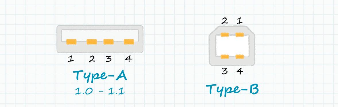
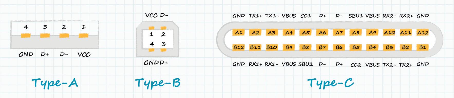
Physical Type A and Type B USB connectors.
USB 1.1
A revised version of the initial standard was released in 1998. Labelled USB 1.1, it matched the data transfer rates of version 1.0, but could also operate at slower speeds for lower bandwidth devices. It was branded as Full Speed. Apple’s iMac G3 adopted the new USB standard and discontinued the use of serial and parallel ports in its machines. This move helped pave the way for wider adoption of the USB protocol by the industry and wide consumer adoption of USB products. Version 1.0 and 1.1 specified the use of standard Type A (rectangular) or Type B (square with bevelled top corners) connectors.
USB 2.0
As the acceptance of PCs and their various peripherals increased in the market, and as the applications got more complex, the need for increased data transfer speed was apparent. USB 2.0 was released in April of 2000 with a data transfer rate of 480 Mbps. However, bus limitations reduced this to 280 Mbps. It was branded for marketing purposes as High Speed. The new version could also operate at 12 and 1.5 Mbps for devices requiring less bandwidth. It also offered plug and play capability for multimedia and storage devices as well as support for power sources using USB connectors up to 5 V and 500 mA.
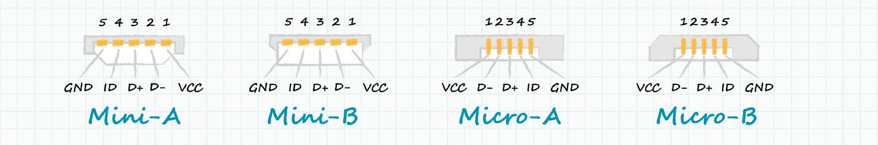
Additionally, it offered the ability for two devices to interact without the need for a separate USB host, also known as USB On-the-Go. USB 2.0 is compatible with USB Type A, B, and C connectors, as well as USB Mini and Micro A & B connectors. The release of Micro A & B connectors, however, did not happen until 2007.
In 2000, the first USB flash drives were also released commercially with up to 8 megabytes of storage capacity, furthering the acceptance of the USB standard. In today’s world, flash drives are available with storage in the terabyte range.
Wireless USB
The wireless USB standard (W-USB) was announced in May of 2005 for wireless short range network communication with a 10-metre range limit and a speed of 480 Mbps. This standard is no longer in use.
USB Micro
USB Micro connectors made their debut in 2007. Essentially smaller versions of the USB Mini-B connectors, they offered quicker charging speeds and data transfer than the mini devices. USB Micro connectors were largely introduced for use in standardising connections in Android mobile devices. Also, it should be clearly stated that the USB Micro connectors are a physical standard, not directly related to the communications standards such as USB 1.0, 1.1, and 2.0.
USB 3.0 (now USB 3.2 Gen 1)
The third major release of the USB standard acknowledged continuing demand for increased digital storage and bandwidth in the market. The USB 3.0 standard was released in November of 2008. It allowed data transfer rates up to a maximum of 5 gigabits per second (Gbps), but typically functioned at around 3 Gbps. This capability led to the standard being branded as SuperSpeedUSB. USB 3.0 doubled the four connection lines of USB 2.0 hardware to eight and allowed for bi-directional transfer of data. It remains backwards compatible with USB 2.0. Since its introduction, USB 3.0 has been updated with 3.2 naming conventions, and is now technically referred to as USB 3.2 Gen 1.
The USB 3.0 standard also increased the power transfer capability to 5 V and 900 mA. It supports physical connectors USB 3.0 Type A & B and USB Type C. To differentiate the connectors used with 3.0, elements in the devices are coloured blue.
Clarifying USB 3.2 naming conventions
Name Maximum Alternate speed name Previous name
USB 3.2 Gen 2x2 20 Gbps SuperSpeed USB 20 Gbps USB 3.2 USB 3.2 Gen 2 10 Gbps SuperSpeed USB 10 Gbps USB 3.1 Gen 2 USB 3.2 Gen 1 5 Gbps SuperSpeed USB 5 Gbps USB 3.1 Gen 1 or USB 3.0
USB 3.1 (or USB 3.2 Gen 2x1)
The USB 3.1 version was an interim standard that is identical to 3.0, except that it increased data transfer rates up to 10 Gbps (USB 3.1 Gen 2). As with USB 3.0, the name for USB 3.1 was updated and is now called USB 3.2 Gen 2. With the upgraded transfer speeds, this earned it the designation SuperSpeed+. Released in July of 2013, version 3.1 used the same connectors (USB A, B, Mini & Micro) as 3.0.
In 2014, USB Type C connectors were also announced. First proposed in 2012, the Type C connector provides data, display, and power signals through a single, small connector that is also reversible. At about one third the size of the original USB Type A connector, the Type C is oval-shaped and somewhat thicker than the USB Mini and Micro versions. It incorporated additional wires and pins that added to its data potential.
USB 3.2 and USB Type C
USB 3.2 replaced the USB 3.0/USB 3.1 standards and made certain retroactive changes to those standards. With a continuing need for increased speed being the driving factor, USB version 3.2, another interim step, was introduced in September of 2017 and effectively doubled the data transfer speed to 20 Gbps (USB 3.2 Gen 2x2) by increasing the data transfer channels from a single lane to two. This was accomplished by adding USB Type C connectors. The increase to 20 Gbps is only possible using USB Type C cables which can transmit 10 Gbps in each direction over two wire pairs.
USB 4.0
USB 4.0, which was released in August of 2019, is based on the Thunderbolt 3 protocol. It features up to 40 Gbps of data transfer and, with the more recent Power Delivery 3.1 standard, power transfer of up to 240 W. Thunderbolt 3 was a protocol developed by Intel in 2015 to support high speed data and video transfer.
The USB 4.0 version does not need new connectors and uses the existing Type C connectors. This allows data and video signals to effectively share lanes and achieve the >
STM32H7
STM32H723/733, STM32H725/735, and STM32H730
• Cortex-M7 core running at the record-breaking frequency of 550 MHz • Up to 1MB internal flash • External memory interface: FMC and Octal SPI memory interface • FMAC (filtering) and Cordic (trigonometric) for mathematical acceleration • Advanced analog peripherals including two 16-bit ADCs and one 12-bit ADC • Interfaces to popular industrial connectivity standards, including three FD-CAN ports,
Ethernet, and Parallel Synchronous Slave Interface • Chrom-ART Accelerator™ for superior graphics performance • Scalable architecture with state-of-the-art cyber protection • Graphic, AI, Security solutions and STM32Cube ecosystem supported
USB physical connector form factors.
maximum bandwidth usage of the device, optimising data transfer speeds. It is also backwards compatible (using adapters) with USB versions 2.0 and 3.2, although speeds will suffer.
This newest version of the USB standard also offers Intelligent Power Delivery, allowing a USB 4.0 cable to deliver as much power as a connected device requires, up to 240 Watts and 5 Amps. Power delivery is also bi-directional, meaning it can flow to or from the connected device.
A word about connectors
As has been mentioned, the different versions of the USB standard have spawned a variety of connectors — 14 so far, to be exact. Even though the physical form factor and the USB protocol are technically independent, there is an interrelationship in regards to which protocols work with particular form factors. With that in mind, here is a quick review of some of the most prominent types used. • USB Type A: the first, and most widelyknown USB connector has been in use since the standard was first released. It has a flat, rectangular shape and is only insertable in one orientation. • USB Type B: smaller than Type A and is square in shape with slightly bevelled corners on the top and a large space on the inside. • USB Mini-B: compact sized, 5-pin connector used in older cell phones and digital cameras, largely replaced by the
Micro-B. • USB Micro-B: smaller and flatter than the Mini-B, used in many smart phones. • USB 3.0 Type A: flat and rectangular similar to Type A, but with square pins and blue internals for identification. Also known as SuperSpeed. • USB 3.0 Type B: designed for Super-
Speed applications, with two stacked rectangular sections and blue internals for identification. • USB 3.0 Micro-B: small, flat and rectangular with two distinct sections. Designed to carry data and power for SuperSpeed applications. • USB Type C: reversible symmetrical design with rectangular shape and rounded corners. Newest USB connector device.
Decoding USB naming conventions
In an attempt to clear up market confusion, beginning with the USB 3.2 standard, the USB-IF has implemented a series of naming changes. The original USB 3.0 and USB 3.1 terms were dropped and replaced by a three-tiered scheme.
The first tier was known as USB 3.2 Gen 1 (previously USB 3.0 and USB 3.1 Gen 1). It was initially branded as SuperSpeed USB, with data transfer rates up to 5 Gbps. The Gen label refers to generation and the number following it refers to the number of data lines. The most recent branding for this has been changed to SuperSpeed USB 5 Gbps.
The second tier is labelled USB 3.2 Gen 2 (formerly USB 3.1 Gen 2). It was initially branded as SuperSpeed 10 Gbps with data transfer up to 10 Gbps. This marketing term remains the same.
The third tier is USB 3.2 Gen 2x2 (formerly USB 3.2). This level was initially branded as SuperSpeed USB 20 Gbps and this term remains in place. It has data transfer speeds up to 20 Gbps.
The USB-IF has also refined the USB 4.0 naming, changing it to USB4 with the following two tiers: • USB4 20 Gbps (data speed matches its naming) • USB4 40 Gbps (data speed matches its naming)
Each of these tiers has a new logo associated with it for use on products. It is hoped that this will help to clear up any consumer confusion in the marketplace. The variety of names for the USB standards continues to cause some concern and confusion in the market, however, as devices are still often referred to under the old naming scheme.
The continuing relevancy of USB
The USB standard served to clear up the hornet’s nest of connectors and cables that were originally used to link peripheral devices to host computers. The ongoing evolution of this standard, and the devices that support it, has meant increased data speeds and power delivery via a small, inexpensive, and easy-to-use interface.
What began as a way to connect peripherals, became a way to improve the user experience with all types of products, including smart phones and other mobile devices, games, toys, smart home products, and industrial networking. USB devices are also frequently used today simply for charging purposes.
These features have helped to make USB the dominant signal transfer technology in use around the world today, while the applications for USB technology will only continue to grow. CUI Devices offers a range of USB connectors and USB cables in various form factors designed to meet multiple USB standards. This article has been reprinted with permission from CUI Devices. It was originally published on the CUI Devices website.
SHORTcircuits
COMMUNICATION SIGNAL DEVELOPED FROM ENVIRONMENTALLY FRIENDLY BATTERY
The NTT Corporation and the Graduate School of Frontier Sciences, the University of Tokyo (GSFS) have produced what is reportedly the world’s first communication signal using a battery and a circuit composed of environmentally friendly materials, free of scarce elements and hazardous substances. As the Internet of Things (IoT) proliferates, all sorts of objects are being transformed into devices, expanding their range of services and applications. However, concerns exist about the environmental impact of the disposal of consumables converted into sensor devices. To address this issue, the NTT is promoting the research and development of devices using materials that have a lot environmental impact once discarded.
NTT and GSFS are exploring improvements to environmentally friendly batteries by eliminating the use of scarce materials and hazardous substances; the two organisations have manufactured a proof of concept (PoC) sensor device made from an environmentally friendly circuit using organic semiconductor technology and have succeeded in generating what is reportedly the world’s first communication signal using these types of sustainable materials. This technology could be used for sensing devices in unsealing detection (for example, in single-use water bottles), sensing devices in pill packages to determine if a patient has forgotten to take their prescribed medication or reducing the environmental impact of observational weather buoys.
In 2018, the NTT manufactured and verified the battery operation of the Return-to-the-Earth-Battery (composed of fertiliser ingredients and organic materials). Then, the collaborators interviewed experts in the field of waste management to determine what materials should be selected to achieve low environmental impact. In response the pair eliminated materials containing scarce elements and hazardous substances. Using these materials, researchers at NTT collaborated with Professor Junichi Takeya’s laboratory at GSFS to create an environmentally friendly circuit. This was achieved by developing an organic transistor manufacturing process in which all electrodes are made of carbon material (carbonelectrode organic transistors) and are used to construct analog oscillation circuits and digital modulation circuits with CMOS. Researchers formed a three-dimensional conductive porous structure, applied carbon as an electrode and increased the voltage by serialising the batteries.
The NTT will continue developing related technologies, collaborating with external organisations and companies to explore use cases unique to ‘low environmental impact’ and jointly implementing novel services. More details about this research are available in Scientific Reports.

STRENGTH IN NUMBERS WHEN IT COMES TO INERTIAL SENSORS
Researchers working in the field of navigation and supported by the Swiss National Science Foundation (SNSF) have developed a method that allows several low-cost inertial sensors working in combination to replace a single expensive sensor.
Inertial sensors such as accelerometers and gyroscopes are used nearly everywhere, from smart watches to submarines, drones, spacecraft, vacuum cleaners and even game controllers. The purpose of these sensors is to indicate the position, speed or direction of an object. Their drawback is their lack of precision, at least when it comes to the low-cost versions used in many devices.
Now there may be a way to solve this problem, with researchers from the University of Geneva reporting that networking several inexpensive sensors is a viable alternative to more powerful sensors. By combining the measurements of several low-cost, individual sensors, the researchers succeeded in obtaining a very precise navigational measurement. Their breakthrough was published in the journal IEEE Transactions on Signal Processing.
“It is as if we had created a virtual sensor, and it is particularly efficient because it uses all the information provided by the individual sensors,” said Yuming Zhang, a PhD candidate in statistics and lead author of the new study. These virtual sensors not only offer the same performance as actual sensors but are also less expensive and can be more flexibly configured. They could therefore be used in a number of consumer devices without increasing their cost.
The idea of combining information from different sensors is not new, but until now technical constraints have limited its application. As explained by Zhang, “Sensor measurement errors are very complex to handle individually, and even more so when several sensors are combined.” The team solved the problem using a new signal decomposition approach, which makes it possible to understand and deal with errors that affect measurements and to process them using a novel statistical method.
According to the researchers, the potential applications of the new technique widely range from aerial mapping using drones to autonomous vehicles. In addition, the ability to optimally combine different sensor technologies could help develop a new generation of global positioning systems.


SHORTcircuits
AUSTRALIAN QUANTUM INDUSTRY POISED TO REACH $6 BILLION BY 2045
Quantum technology is forecast to reach $6 billion and generate more than 19,000 jobs in Australia by 2045, according to updated market projections released by CSIRO, Australia’s national science agency. CSIRO’s original Growing Australia’s Quantum Technology Industry Roadmap has been updated two years on and reflects the growth trajectory of quantum technology across the report’s three key domains of quantum computing, sensing and measurement, and communications. The report provides estimates and refinements of the original modelling and extends the forecast from 2040 to 2045 while affirming the economy results from the earlier report.
CSIRO Senior Economist Mingji Liu said that the updated figures reflected recent domestic and global developments in quantum technology opportunities. “Our updated modelling reaffirms that quantum technology continues to be a significant opportunity for Australia in the years to come. Although there is still uncertainty as to how quantum technology will be commercialised both around the world and domestically, the startup funding and investment in quantum is encouraging,” Liu said.
The economic modelling forecasts that by 2030, Australia’s quantum technology opportunity in revenue terms could conservatively reach $2.2 billion and could generate 8700 jobs. In five years, this could reach $3.3 billion by 2035, and then reach $4.6 billion by 2040 and could generate 16,100 jobs (the same as original projections in 2020). According to CSIRO Quantum Technologies Director Jim Rabeau, the last 18 months have seen a significant increase in focus to strengthen Australia’s position in the emerging global quantum industry. “CSIRO has launched its Future Science Platform, a number of new companies have been backed or reached key milestones, a tech industry group has been formed and we’re seeing an intensive national focus. The key now will be to sustain and grow over the long term,” Rabeau said.
CSIRO Chief Executive Larry Marshall said that Australia is at a pivotal stage of growing its quantum industry and is at a tipping point between research and commercial development. “We need to harness our bold vision for what this breakthrough technology could mean for some of our largest industries,” Marshall said.
Image credit: CSIRO
Australia has strong research capabilities in quantum hardware development and quantum information science, both of which are critical to the development of the hardware and software stack needed to enable functional quantum computing applications.
PHYSICISTS DESIGN NEW TYPE OF UNIVERSAL QUANTUM COMPUTER
The computing power of quantum machines is low and increasing it can be challenging. Physicists from the University of Innsbruck have presented a new architecture for a universal quantum computer that overcomes such limitations and could be the basis of the next generation of quantum computers.
Quantum bits (qubits) in a quantum computer serve as a computing unit and memory at the same time. Because quantum information cannot be copied, it cannot be stored in a memory as in a classical computer. Due to this limitation, all qubits in a quantum computer must be able to interact with each other; this still presents a challenge for building powerful quantum computers. In 2015, theoretical physicist Wolfgang Lechner, together with Philipp Hauke and Peter Zoller, proposed a new architecture for a quantum computer, now named LHZ architecture after the authors. According to Lechner, the architecture was originally designed for optimisation problems, but in the process, the physicists reduced the architecture to a minimum in order to solve these optimisation problems as efficiently as possible. The physical qubits in this architecture do not represent the individual bits but encode the relative coordination between the bits. “This means that not all qubits have to interact with each other anymore,” Lechner said.
Lechner has now shown that this parity concept is also suitable for a universal quantum computer. Parity computers can perform operations between two or more qubits on a single qubit. “Existing quantum computers already implement such operations very well on a small scale. However, as the number of qubits increases, it becomes more and more complex to implement these gate operations,” said Michael Fellner, one of the scientists on Lechner’s team.
In two publications in Physical Review Letters and Physical Review A, the Innsbruck scientists have shown that parity computers can, for example, perform quantum Fourier transformations — a fundamental building block of many quantum algorithms — with fewer computation steps and thus more quickly. “The high parallelism of our architecture means that, for example, the well-known Shor algorithm for factoring numbers can be executed very efficiently,” Fellner said.
The new concept also offers hardware-efficient error correction; because quantum systems are very sensitive to disturbances, quantum computers must correct errors continuously. Significant resources must be devoted to protecting quantum information, which increases the number of qubits required.
CEA’S RF CHIP ENABLES IoT CONNECTIVITY FOR REMOTE DEVICES
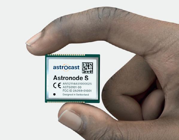
CEA, a French technology-research organisation, and Astrocast, a global satellite Internet of Things network operator, have announced their successful collaboration on a low-cost, bidirectional communication module that enables corporations to communicate with their remote assets in areas not covered by terrestrial networks.
The module’s L-band chip, based on a new architecture developed by CEA’s Laboratory of Electronics Information Technology (CEA-Leti), is a key hardware component that enables Astrocast customers to benefit from cost-efficient communication with their assets in the field through its network. Completed earlier this year in an expedited project between the research institute and Astrocast, it is embedded in Astrocast’s RF module, Astronode S.
The chip’s architecture is split over the RF core and digital processing and control units. It is fully optimised to support Astrocast’s dedicated bidirectional ground-to-satellite protocol and provides an optimal trade-off between link budget and low-power and low-cost constraints. The chip also embeds all low-Earth orbit (LEO), satellite-specific features such as satellite detection and robustness to Doppler shift.
The miniaturised, surface-mount module communicates with terrestrial devices via Astrocast’s constellation of LEO satellites. Using the L-band spectrum, the network primarily targets maritime, oil and gas, agriculture, land transport and environmental applications in which ubiquitous coverage is required.
“Terrestrial IoT networks cover only about 15%, which leaves vast remote and rural areas where our global satellite network provides coverage that is crucial for our target markets,” said Laurent Vieira de Mello, COO, Astrocast. “Leveraging its expertise embedded in a preliminary version of the RF chip, CEA-Leti developed its chip and delivered the final prototype to meet our requirements and timeto-market goals. They managed the chip technology transfer to our industrialisation, qualification and production partner.”
The project was managed through a flexible collaboration model covering both prototype and industrialisation phases. Michael Durr, Business Development Manager at CEA-Leti, said: “An accelerated time-to-market goal drove this project … We pioneered this RF technology in 2019, and our team customised it for Astrocast up to production in only three years.”