


Today’s electronic engineers are challenged by multiple factors. Research over the years has illustrated common trends that you, as engineers, deal with including keeping your skills up-to-date, shrinking time-to-market windows, fewer engineers and smaller design teams for large projects and evolving technological trends. The bottom line is that you must continually update your engineering knowledge base to be successful in your work.

Throughout 2023, we are presenting a series of online educational days where you can learn how to address specific design challenges, learn about new techniques, or just brush up your engineering skills. We are offering eight different Training Days. Each day will focus on helping you address a specific design challenge or problem. These are not company sales pitches! The focus is on helping you with your work.
For more information and to register for these webinars, go to:
EETRAININGDAYS.COM
AVAILABLE ON DEMAND THERMAL MANAGEMENT
JUNE 14TH DESIGNING FOR SUSTAINABILITY
JULY 12TH EMI/RFI/EMC
AUGUST 9TH BATTERY MANAGEMENT
SEPTEMBER 13TH MOTOR DRIVES DESIGN
OCTOBER 11TH IOT DESIGN / WIRELESS

NOVEMBER 8TH ELECTRIC VEHICLE DESIGN
DECEMBER 6TH 5G / RF DESIGN

Welcome to EE World’s 5G, Wireless, and Wired Communications Handbook. What’s this? A longer name compared to 2021 and 2022? In truth, we at EE World have for years covered many forms of electrical communications. It’s time the handbook name better describes what we do.
5G is much more than cellular radio. There’s an entire network behind it. The electrical and optical links that form these networks continue to gain speed and capacity. Research is now underway to bring 224 Gb/sec data lanes over copper. At the same time, silicon photonics and co-packaged optics have moved into manufacturing. We’ll investigate these trends later in 2023 and beyond.
People who build networks, operate them, and develop applications demand more throughput, which falls on engineers to deliver. After all, network architects, software developers, IT people, telecom operators, and everyone else assume that the bits arrive at their destinations on time and intact. We don’t. We know bits don’t magically traverse networks. They need transmitters, receivers, signal processing, timers, and layers of protocols. As new network configurations such as Open RAN appear, they come with new wired connections. Disaggregating radio-access networks into open systems means more opportunities for interoperability problems. One such connection is the E2 interface, explained in “How does 5G’s O-RAN E2 interface work?”
Bits must arrive on time and in sync. For the third year, we’re delivering two articles on network timing in this handbook. We’ve also published other timing articles in between handbooks. You can find them all, plus timing products, at http://www.5gtechnologyworld.com/category/timing.
Wireless and wired networks deliver connectivity to the world, but what’s connectivity without connectors and cables? “Connectors and cables modernize data centers” delves into space constraints, signal integrity, cabling, and thermal-management issues in data centers. It’s up to EEs to solve those problems.

In this issue, you’ll also learn that just having a functioning network isn’t enough. 5G, like all networks, needs protection from electrical hazards. “How to safeguard cellular base stations from five electrical hazards” shows you how to use circuit-protection devices such as fuses and TVS diodes to keep circuits safe.
As if protection from electrical hazards wasn’t enough, networks can suffer from RF interference as well. One form of which is passive intermodulation (PIM) caused by nonlinearities in connectors, cables, and so on. Locating PIM problems in the field requires test equipment and expertise.
Even as 5G continues to deploy, researchers are looking into how to make marketers’ dreams come true. Having attended 6G conferences for a few years now, I can report that people already want more — and less — from wireless networks. They want a better user experience for consumers, lower latency for machines, more computing power for digital transformation, and the “metaverse,” whatever that is. Of course, we all want more while using less energy. Two articles in this handbook look at 6G. One covers channel sounding at frequencies above 100 GHz. Another looks at how 6G networks will need to operate more sustainably than does 5G.
As engineers, it falls on us to provide the infrastructure that makes it all happen.
Measuring just 0.47 x 0.28 mm, with an ultra-low height of 0.35 mm, our new 016008C Series Ceramic Chip Inductors offer up to 40% higher Q than all thin film types: up to 62 at 2.4 GHz.
High Q helps minimize insertion loss in RF antenna impedance matching circuits, making the 016008C ideal for high-frequency applications such as cell phones, wearable
devices, and LTE or 5G IoT networks.
The 016008C Series is available in 36 carefully selected inductance values ranging from 0.45 nH to 24 nH, with lower DCR than all thin film counterparts.
Find out why this small part is such a big deal. Download the datasheet and order your free evaluation samples today at www.coilcraft.com.
Once again, Coilcraft leads the way with another major size reduction in High-Q wirewound chip inductors
22 Open RAN networks pass the time
Network elements must meet certain frequency, phase, and time requirements to ensure proper end-to-end network operation. Synchronization architectures defined by the O-RAN alliance dictate how Open RAN equipment can meet these requirements.
24 How timing propagates in a 5G network
5G’s high speeds place extreme demands on the components that maintain accurate time.
Compliance with industry timing standards calls for accuracy in the face of temperature changes, shock, and vibration.
27 Connectors and cables modernize data centers
Demands for bandwidth-intensive, data-driven services are fueling a rise in compute, data storage, and networking capabilities. These rises put pressure on connectors and cable to deliver data at higher speeds with better signals and less heat.
30 How to safeguard cellular base stations from five electrical hazards
Circuit-protection components such as fuses and TVS diodes protect power and data circuits from damage. Here’s where and how to insert them into your circuits.
34 Experiments bring hope for 6G above 100 GHz
Efforts to explore and “unlock” this frequency region require an interdisciplinary approach with high-frequency RF semiconductor technology. The THz region also shows great promise for many application areas ranging from imaging to spectroscopy to sensing.
37 5G mmWave test builds on RF best practices
The high level of integration in today’s mmWave phone means traditional test methods no longer apply.
40 6G promises to bring sustainability to telecom
Sustainability is at the heart of 6G research, not just in telecom networks and equipment, but throughout the supply chain.
43 How does 5G’s O-RAN E2 interface work?
RAN intelligent controllers, as defined by O-RAN Alliance, let cellular operators deploy intelligent RAN optimization applications. E2 is a key interface defined by O-RAN Alliance, but there are challenges in practically using it.
EDITORIAL
VP, Editorial Director
Paul J. Heney pheney@wtwhmedia.com @wtwh_paulheney

Editor-in-Chief
Aimee Kalnoskas akalnoskas@wtwhmedia.com @eeworld_aimee
Senior Technical Editor Martin Rowe mrowe@wtwhmedia.com @measurementblue
Associate Editor Emma Lutjen elutjen@wtwhmedia.com
Executive Editor Lisa Eitel leitel@wtwhmedia.com @dw_LisaEitel
Senior Editor Miles Budimir mbudimir@wtwhmedia.com @dw_Motion
Senior Editor Mary Gannon mgannon@wtwhmedia.com @dw_MaryGannon
Managing Editor Mike Santora msantora@wtwhmedia.com @dw_MikeSantora
VIDEOGRAPHY SERVICES
Videographer Garrett McCafferty gmccafferty@wtwhmedia.com
Videographer Kara Singleton ksingleton@wtwhmedia.com
WTWH Media, LLC
1111 Superior Ave., Suite 2600 Cleveland, OH 44114
Ph: 888.543.2447
FAX: 888.543.2447
CREATIVE SERVICES & PRINT PRODUCTION
VP, Creative Services Mark Rook mrook@wtwhmedia.com @wtwh_graphics
VP, Creative Services Matthew Claney mclaney@wtwhmedia.com @wtwh_designer
Art Director Allison Washko awashko@wtwhmedia.com @wtwh_allison
Senior Graphic Designer Mariel Evans mevans@wtwhmedia.com @wtwh_mariel
Director, Audience Development Bruce Sprague bsprague@wtwhmedia.com
PRODUCTION SERVICES
Customer Service Manager Stephanie Hulett shulett@wtwhmedia.com
Customer Service Representative Tracy Powers tpowers@wtwhmedia.com
Customer Service Representative JoAnn Martin jmartin@wtwhmedia.com
Customer Service Representative
Renee Massey-Linston renee@wtwhmedia.com
Customer Service Representative Trinidy Longgood tlonggood@wtwhmedia.com
MARKETING
VP, Digital Marketing Virginia Goulding vgoulding@wtwhmedia.com @wtwh_virginia
Digital Marketing Coordinator
Francesca Barrett fbarrett@wtwhmedia.com @Francesca_WTWH
Digital Design Manager Samantha King sking@wtwhmedia.com
Marketing Graphic Designer Hannah Bragg hbragg@wtwhmedia.com
Webinar Manager Matt Boblett mboblett@wtwhmedia.com
Webinar Coordinator

Emira Wininger emira@wtwhmedia.com
Events Manager
Jen Osborne jkolasky@wtwhmedia.com @wtwh_Jen
Events Manager

Brittany Belko bbelko@wtwhmedia.com
Event Marketing Specialist Olivia Zemanek ozemanek@wtwhmedia.com
Event Coordinator Alexis Ferenczy aferenczy@wtwhmedia.com
Web Development Manager B. David Miyares dmiyares@wtwhmedia.com @wtwh_WebDave
Senior Digital Media Manager Patrick Curran pcurran@wtwhmedia.com @wtwhseopatrick
Front End Developer Melissa Annand mannand@wtwhmedia.com
Software Engineer David Bozentka dbozentka@wtwhmedia.com
Digital Production Manager Reggie Hall rhall@wtwhmedia.com
Digital Production Specialist Nicole Lender nlender@wtwhmedia.com

Digital Production Specialist Elise Ondak eondak@wtwhmedia.com
Digital Production Specialist Nicole Johnson njohnson@wtwhmedia.com
FINANCE
Controller Brian Korsberg bkorsberg@wtwhmedia.com
Accounts Receivable Specialist Jamila Milton jmilton@wtwhmedia.com
DESIGN WORLD does not pass judgment on subjects of controversy nor enter into dispute with or between any individuals or organizations. DESIGN WORLD is also an independent forum for the expression of opinions relevant to industry issues. Letters to the editor and by-lined articles express the views of the author and not necessarily of the publisher or the publication. Every effort is made to provide accurate information; however, publisher assumes no responsibility for accuracy of submitted advertising and editorial information. Non-commissioned articles and news releases cannot be acknowledged. Unsolicited materials cannot be returned nor will this organization assume responsibility for their care.
DESIGN WORLD does not endorse any products, programs or services of advertisers or editorial contributors. Copyright© 2023 by WTWH Media, LLC. No part of this publication may be reproduced in any form or by any means, electronic or mechanical, or by recording, or by any information storage or retrieval system, without written permission from the publisher.
SUBSCRIPTION RATES: Free and controlled circulation to qualified subscribers. Non-qualified persons may subscribe at the following rates: U.S. and possessions: 1 year: $125; 2 years: $200; 3 years: $275; Canadian and foreign, 1 year: $195; only US funds are accepted. Single copies $15 each. Subscriptions are prepaid, and check or money orders only.
SUBSCRIBER SERVICES: To order a subscription or change your address, please email: designworld@omeda.com, or visit our web site at www.designworldonline.com
POSTMASTER: Send address changes to: Design World, 1111 Superior Ave., Suite 2600, Cleveland, OH 44114


Wireless system design complexity keeps increasing, from mobile wireless technology moving from 3G and 4G to the expansive use cases of 5G, and the introduction of Industry 4.0. Driven by the need to optimally manage the sharing of valuable resources to an expanding set of users, a growing number of engineers are turning to artificial intelligence (AI) to solve the challenges introduced by modern systems.
From optimizing call performance through resource allocation to managing vehicle-to-vehicle (V2V) and vehicle-to-everything (V2X) communication between autonomous cars, AI has brought the sophistication necessary for today’s modern wireless applications. As the number and capabilities of those devices connected to networks expands, so too will the role of AI in wireless. For the future success of the technology, engineers should be aware of the key benefits and applications of AI in today's wireless systems, as well as the best practices necessary for optimal implementation.

Three distinct use-cases have defined mobile networks’ transition to 5G and have acted as the driving forces in engineers’ adoption of AI. These include:
• The optimization of speed and quality of mobile broadband networks,
• The need for ultra-reliable low rates, and
• Massive machine-type communication for time-sensitive connections between Industry 4.0 devices.
An expanding set of devices competing for the resources of the same network and an ever-increasing pool of users also leads to the increasing complexity of wireless systems. Formerly linear patterns of designs once understood by human-based rules and human processing of data are no longer sufficient. AI techniques, however, can overcome non-linear problems by extracting patterns automatically and efficiently. These techniques can do so beyond the ability of human-based approaches.
Integrating AI in a wireless environment enables machine learning and deep learning systems to recognize patterns within communications channels. These systems then optimize the resources given to that link to improve performance. As applications of a modern network compete for the same resources without the use of AI methodologies, managing these networks becomes a nearly impossible task.
The sophistication of AI also enables more efficient project management such as reduced order modelling. By incorporating simulated environments into an algorithmic model through estimating the behaviour of source environments, engineers can quickly study a system’s dominant effect using minimal computational resources. Additional benefits to the use of AI in this context can include more time to explore design and carry out more iterations faster, cutting time in production cycles and associated costs.
AI techniques can overcome nonlinear problems by extracting patterns automatically and efficiently.
MathWorks
Data quality is vital for the successful and effective deployment of AI. AI models need to be trained with a comprehensive range of data to adequately deal with real-world scenarios. Applications provide the data variability necessary for 5G network designers to train AI robustly by synthesizing new data based on primitives or by extracting them from over-theair signals. Failure to explore a large training data set and iterate on different algorithms based on that data could result in a narrow local optimization instead of an overall global one, compromising the reliability of AI in realworld scenarios.
A robust approach to testing AI models in the field is similarly critical to success. If signals to test AI are captured only in a narrow and localized geography, the lack of variability in that training data may negatively impact how an engineer may approach and optimize their system design. Without comprehensive field iterations, the parameters of individual cases cannot be used to optimize AI for specific locations, adversely impacting call performance.
Digital transformation has been embraced in industries across the spectrum, from telecommunications to automotive. This increased adoption of transformation has necessitated the widescale adoption of AI and is the primary driver for its application.
Placing electronic communications in areas once mechanically orientated generates large amounts of data as applications that include smart homes, telecommunication networks, and autonomous vehicles (AV) connect. The large quantities of data generated by these applications facilitates the development of future-looking AI techniques to accelerate the process of digital transformation, yet also stretches the resources of the joining network.
In telecommunications, AI is deployed at two levels—at the physical layer (PHY) and above PHY. The application of AI for improving call performance between two users is referred to as operating at PHY. Applications of AI techniques to physical layers include digital pre-distortion, channel estimation, and channel resource optimization. Additional applications include autoencoder design that spans automatic adjustments to transceiver parameters during a call. Figure 1 shows a roadmap for using data and AI to train models.
Channel optimization is the
enhancement of the connection between two devices, principally network infrastructure and user equipment such as handsets. Using AI helps to overcome signal variability in localized environments through processes such as fingerprinting and channel state information compression.
With fingerprinting, AI can optimize positioning and localization for wireless networks by mapping disruptions to propagation patterns in indoor environments, caused by individuals entering and disrupting the environment. AI then estimates, based on these individualized 5G signal variations, the position of the user. In so doing, AI overcomes traditional obstacles associated with localization methods using comparisons between received signal strength indication (RSSI) and the RSS in providers’ databases. Channel state information compression, on the other hand, is the use of AI to compress feedback data from user equipment to a base station. This ensures that the feedback loop informing the station’s attempt to improve call performance does not exceed the available bandwidth, leading to a dropped call.
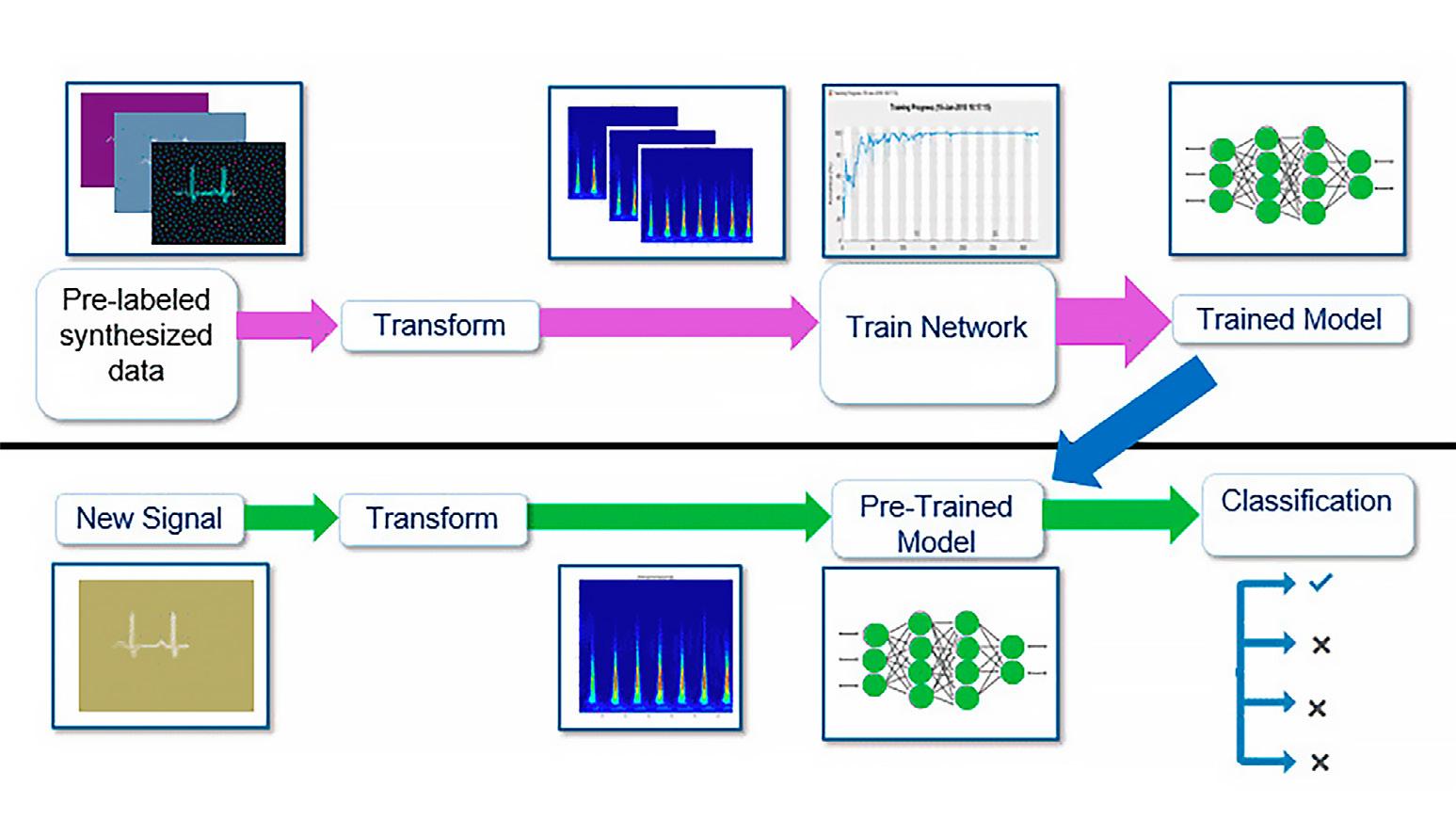
Above-PHY uses are primarily in resource allocation and network management. As the number of users and use cases on the network exponentially increases, network designers are looking to AI techniques to respond to allocation demands in real time. Applications such as beam management, spectrum allocation, and scheduling functions are used to optimize the management of a core system’s resources for the competing users and use cases of the network.
In the automotive industry, using AI for wireless connectivity makes safer autonomous driving possible. Autonomous vehicles and V2V/V2X vehicular communications rely on
data from multiple sources, including LiDAR, radar, and wireless sensors, to interpret the environment. The hardware present in AVs must handle data from these competing sources to function effectively. AI enables sensor fusion (fusing competing signals to allow the vehicle’s software to make sense of its location and establish how it will interact with its environment by understanding omnidirectional messages).
This approach to communications allows the vehicle to establish a 360-degree field of “awareness” of other vehicles (Figure 2) and potential crash threats within its proximity. Whether through informing the driver for the vehicle or driving autonomously, utilization of AI is leading to improved road traffic safety and reducing the number of crashes at intersections.
As the use cases for wireless technology expand, so too does the need to implement AI within those systems. From 5G, to AV, to IoT, these applications would not have the sophistication necessary to function effectively without the use of AI. AI’s place in the engineering landscape, particularly wireless system design, has been growing exponentially in recent years and this pace of change can be expected to continue rising – and faster – as the use cases and the number of network users expand in the modern age.
5G’s orthogonal frequency division multiplexing (OFDM) brings with it a major design challenge, namely an inherent wide dynamic variation between a signal’s peak and the average power. The peak-toaverage power ratio (PAPR) leads to inefficient transmission performance. That’s because the OFDM waveform is created by the sum of multiple sinusoidal signals that can exhibit constructive and destructive behaviour. As a result, at some time instances, the ratio between the maximum signal power to its average will become high. A signal with high PAPR will cause a power amplifier (PA) to operate in its non-linear region.
A high PAPR creates two problems. First, outof-band distortion leads to adjacent-channel interference and spectral emission mask (SEM) violations. Second, in-band distortion degrades the throughput performance. To tackle these problems, a radio’s power amplifier (PA) needs to operate below its 1 dB compression point (P1dB). That backing off improves linearity at the cost of reduced PA efficiency. We need a PAPR reduction technique to let the PA operate at high efficiency while maintaining good linearity.
Several techniques that reduce the PAPR of the OFDM signal have been proposed. There are two main categories for these techniques: distortion-based methods, which result in out-of-band distortion, and distortionless methods. This article defines PAPR in more detail and introduces the techniques to reduce PAPR. The article will also discuss some of the challenges to reduce the PAPR in multi-operator network use cases.
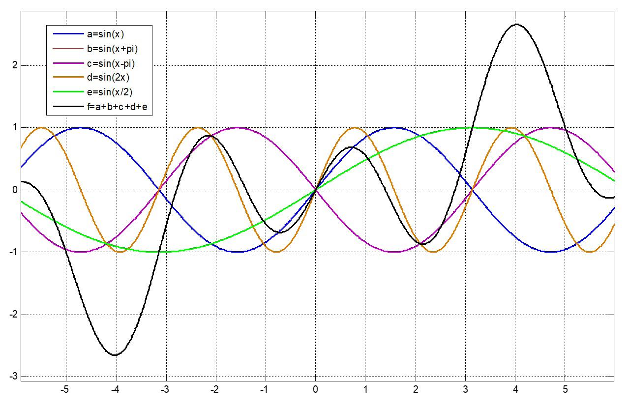
An OFDM waveform is created by the summation of multiple sinusoidal signals. Figure 1 shows that constructive interference between the sinusoids occurs when the individual sinusoids reach their maximum values at the same time. This constructive
interference will cause the output envelope of the OFDM waveform to suddenly rise, producing high peaks generated from the constructive characteristic. At other times, destructive interference will occur. In that case, the individual sinusoids will cancel out one another, resulting in troughs in the OFDM waveform output envelope. Furthermore, in the example of Figure 1, the sinusoids are
constant amplitude. The amplitudes of the sinusoids will, however, vary dynamically. This amplitude variation, combined with the destructive interference, results in a low average output envelope. Hence, the OFDM waveform features high PAPR.
As Figure 2 shows, when a multicarrier signal of very wide dynamic requirement with high PAPR such as an OFDM signal is fed into
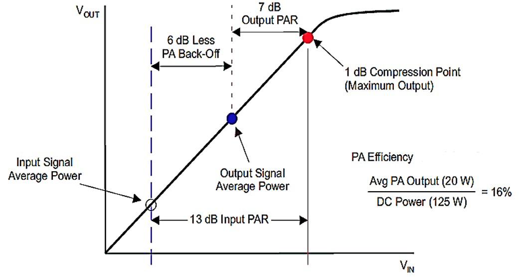
a PA, the PA operates in its nonlinear region. Doing so results in out-of-band distortion, which violates the spectrum emission mask (SEM), disrupts other adjacent channels, and creates unwanted radiation. At the cellular system level, this causes poor coverage, dropped calls, and low quality of service. Backing off the power to avoid PA compression will result in lower power efficiency and cell coverage. A promising solution would reduce PAPR. In Figure 2, the PAPR of the input signal is 13 dB. A PAPR reduction technique can reduce this to 7 dB, allowing 6 dB less back off, which results in a significant PA efficiency improvement.
High PAPR is a major practical problem involving multi-carrier signals such as an OFDM signal. If A = (A0,A1, ...,A(N-1)) is a modulated data sequence of length N in time interval (0,t), where Ai is a symbol from a signal constellation and t is symbol duration, then the N carrier OFDM envelope is given by
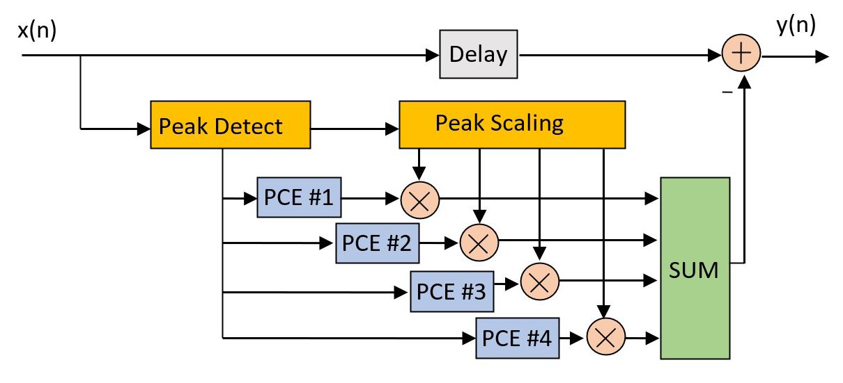
Figure 3. The peakcancellation technique uses peak detection and filtering to reduce peaks created when peaks in OFDM sinusoids align.
where and . The PAPR of a transmitted signal, , is the ratio of the maximum power and the average power of the signal and can be defined by:

called scrambling techniques, require some side information sent to the receiver device, adding complexity to the system. Moreover, this protocol is not defined by the 3GPP for user equipment. Techniques such as Partial Transmit Sequence (PTS) and Selected Mapping (SLM) fall into this category. These techniques are, however, not practical in 4G and 5G mobile systems. Hence, the distortion-based techniques are more attractive [1]. Here we review the peak cancellation technique used widely in wireless communication systems.
amplitude. Each PCE is occupied for the duration of the filter length and the incoming peaks should wait until the process of the PCE is completed. Finally, all the PCE outputs are accumulated and subtracted from the delayed input signal.
The PC’s main drawback is that it requires a minimum of two stages to achieve the required performance mandated in 3GPP. Hence, the complexity and latency will increase. The number of stages will increase for larger bandwidth and in multi carrier applications.
where E denotes the expectation operator, which calculates the signal’s average amplitude.


The other parameter to consider is crest factor, which is widely used in the literature, and is defined as the square root of the PAPR.
Until now, many techniques have been proposed to reduce high PAPR in communication systems. In general, these techniques can be separated into two categories, distortion-based and distortionless. In the former category, some distortion that violates the spectral emission mask (SEM) will occur. Techniques such as clipping, noise shaping, peak windowing, and peak cancellation fall into this category. As the aim in the system design is to maximise efficiency, it can tolerate some distortion.
Distortionless techniques, sometimes
Figure 3 shows the most promising PAPR reduction technique: peak cancellation (PC). Following the peak detection, the selected peaks are allocated to a peak cancellation engine (PCE). Each PCE gets the amplitude of the peaks and creates a scaling pulse by multiplying the peak phase by the filtered
Modern 5G systems present several challenges for PAPR reduction implementation.
Increasing the number of component carriers (CCs) creates more peaks in the selected window in the time domain signal envelope.
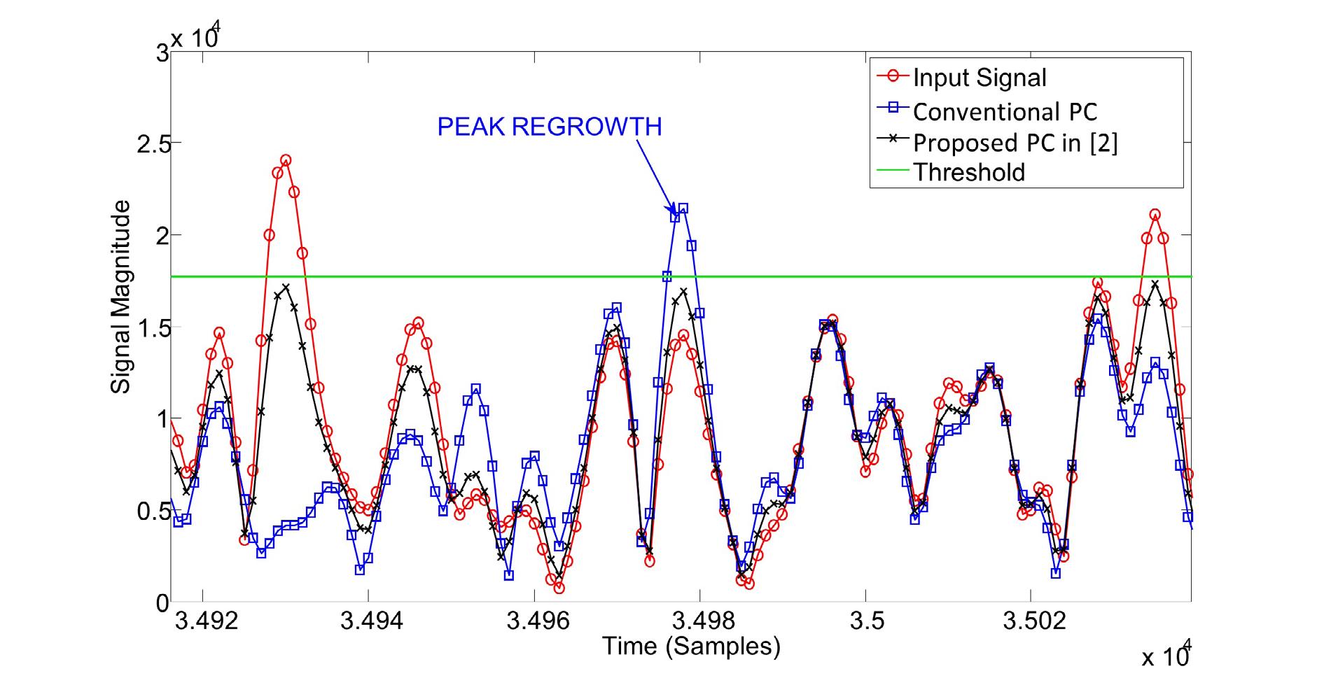
Those peaks cannot be compensated in one or two stages, requiring additional stages in the PAPR implementation. Especially in the inter-band carrier aggregation scenarios, where there is a large gap between the CCs, there will be several contiguous peaks in each selected window above the threshold. Applying the PC technique on these signals results in high error-vector magnitude (EVM). Selecting these peaks and applying filters requires more careful consideration to meet the EVM requirements. One technique to tackle this issue is proposed in [2].
Figure 4 shows the result of a clipped signal with conventional PC and with the proposed PC. Clearly, when there is no spacing between contiguous peaks in the selected window, as is the case in the conventional PC, peak regrowth occurs that can exceed the threshold. This results in spectral-emission violation and EVM degradation. The proposed PC results in suppressed peak regrowth because the spacing removes the possibility of overlapping in the finite impulse response (FIR) filter sidelobes.
End-to-end latency is one of the important factors in providing users with a quality experience, especially in 5G services such as ultra-Reliable Low Latency Communication (uRLLC). The peak cancellation technique requires several stages to reduce the high peaks in the signal. The latency contribution of the peak cancellation technique can be as high as 10 µs. That’s roughly 10% of the total latency specified in 3GPP Release 15.
Increasing the number of stages in the peak cancellation can increase the complexity and the power consumption of the system. Particularly when implemented in an FPGA, the complexity of this implementation increases the system cost.
EVM is one of the imperative metrics to measure the quality of the transmitted signal in a base station. Implementing the peak cancellation results in a tradeoff between the PAPR reduction capability and EVM performance. This is also important from the fact that greater PAPR reduction translates to better power amplifier efficiency. While achieving higher PAPR reduction is desirable,
EVM performance requirement must still be met. Increasing the PAPR reduction means that the threshold level in the peak cancellation needs to be lower, which results in much larger number of peaks detected in a search window. To avoid EVM degradation and peak regrowth, only contiguous peaks at some distance from each other can be selected and passed through the peak engines. It is important to know that peak regrowth is created from the contiguous peaks. That’s because the input signal of the PC is an up-sampled signal and hence the contiguous peaks can exceed the threshold at the same time. The peak regrowth causes spectral leakage or out of band radiation and EVM deterioration.
Most communication systems require PAPR reduction. A high PAPR signal, once transmitted to a power amplifier, creates spectral regrowth that violates the spectral emission mask and deteriorates a network’s throughput performance. PAPR reduction techniques are that required to overcome this issue and increase power amplifier efficiency. Implementing PAPR reduction techniques in modern wireless systems requires careful consideration and some tradeoffs.
[1] P. Varahram et al., Power Efficiency in Broadband Wireless Communications, CRC Press, 2014.
[2] P. Varahram et al., Power amplifiers, US Patent, Patent number 20210184630, 2021.
Pooria Varahram is Research and Development Principal Engineer at Benetel. He holds a PhD in wireless communication systems from University of Putra Malaysia. His main expertise is in digital front-end and signal processing techniques.
In today’s connectivity-driven world, the data center has risen to a place of unprecedented importance. At the same time, technologies such as machine learning have placed intense computational demands and the requirement of faster data access for platforms such as 5G. These conditions place an unsustainable strain on data center infrastructure.
By Scott Schweitzer, AchronixTo address this issue, engineers are re-imagining the very hardware on which the data center is built. Out of this effort, one of the most important technologies that has emerged is the SmartNIC. Dell’Oro Group predicts that the SmartNIC market will become a $2B market by 2027 [1].
In this article, we explore the SmartNIC; what it is, how it rose to prominence, and how it can be designed into a data center system to unlock future benefits.
Before understanding the SmartNIC, we must first discuss the fundamentals of its predecessor: the network interface card (NIC).
From a functional perspective, NICs have historically been an essential board or chip in computing systems, enabling connectivity in internet-connected systems [2]. Also known as network adapters, NICs are used in computer systems, such as personal computers or servers, to establish a dedicated communications channel between the system and a data network. NICs act as translators, taking host memory buffers and formatting them for transmission over a network as structured packets, typically Ethernet. NICs also receive data packets from the network and turn them into memory buffers for applications on the host. Interestingly, all data transiting a network is always represented as character data, regardless of how complex the data structure is or the number of significant digits in a decimal number. This is because the earliest data networks, like ARPANET (1969), were built using standards that had been carried forward from earlier technologies like Telex (1933), which used a 5-bit code created in the 1870s by Emile Baudot [3]. To be clear, ARPANET used 7-bit ASCII (1963); today, we use UTF-8 (8-bit), which is backward compatible with ASCII.
From a hardware perspective, a NIC consists of several key circuit blocks [4]. Some of the most important blocks include a controller for processing received data and ports for a bus connection (e.g., PCIe) within the larger system. With this hardware, the NIC implements the physical layer circuitry necessary to communicate with a data-link-layer standard, such as Ethernet. Operating as an interface, NICs transmit signals at the physical layer and work to deliver the data packets at the network layer.
Now, servers rely on NICs to establish network connectivity, but current changes in the industry will render basic NICs obsolete for server use.
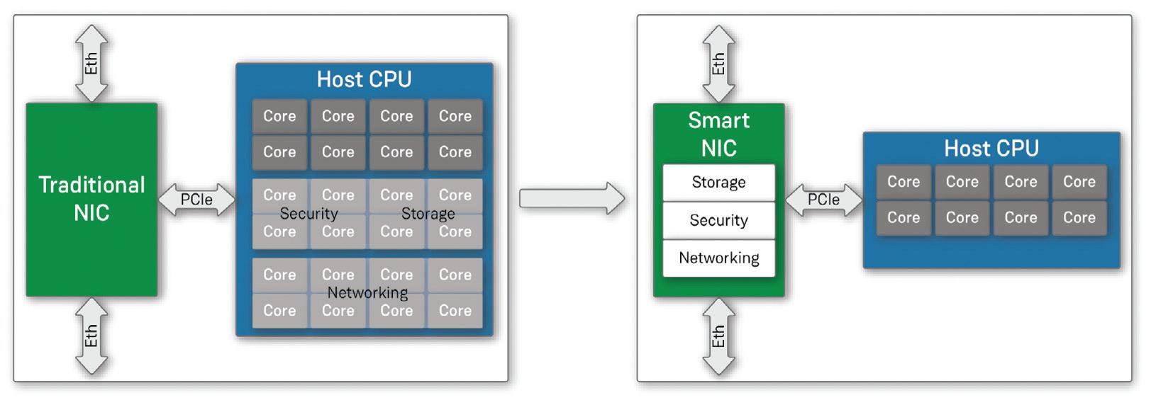
Learn the basics about SmartNICs, their design, and why they’ll be a crucial element in future networks.Figure 1. Compared to a traditional NIC, a SmartNic adds storage, security, and networking features, removing them from the host CPU.
The proliferation of cloud computing and a general increase in internet traffic inundate data centers with growing data and computational tasks. Meanwhile, hardware is getting bogged down by the rise of data and compute-intensive applications such as machine learning, which are placing a greater strain on the computing hardware within the data center. To further confound the matter, the industry is simultaneously pushing towards faster data rates with technologies such as 5G, and soon 6G.
The result: existing data center hardware can no longer keep up with these demands. Workloads accelerate faster than CPUs can handle; the virtualization and microservices running in the data center are quickly becoming unmanageable.
Data center architects have realized that the processing requirements needed to serve the network have become too great for conventional NIC-based architectures. Instead, to achieve high performance without sacrificing power or complexity, we need to offload complex networking tasks
from the server CPUs to dedicated accelerator blocks.
As many in the industry see it, the answer to these problems is the SmartNIC.
At a high level, SmartNICs are NICs augmented with a programmable data processing unit (DPU) for network data acceleration and offloading. The name SmartNIC and DPU are often used interchangeably. The SmartNIC adds extra computing resources to the NIC to offload tasks from the host CPU, freeing up the host CPU for more important tasks.
Early SmartNIC implementations used register-driven ASIC logic. These designs tend to have higher performance in terms of extremely low latency, high packet throughput, and low power consumption—the latter ranging from 15 W to 35 W. Despite the performance benefits, however, they lacked the programmability and flexibility required, often utilizing esoteric commandline tools to set registers. They lacked any meaningful way to programmatically manage packet and flow complexity.
SmartNICs are used in many different deployments, including storage, security, and network processing. Some specific tasks that a SmartNIC may be responsible for include overlay tunneling protocols such as VxLAN and complex virtual switching from server processors [5]. As shown in Figure 1, the eventual goal is to have a solution that consumes fewer host CPU processor cores and, at the same time, offers higher performance at a reduced cost.
Taking a deeper look at a SmartNIC, we find that the programmable packet pipeline consists of many individual hardware accelerator blocks, all optimized for high-performance and low-power networking tasks. Depending on variables such as application and cost, there are many different SmartNIC implementations, each with its own benefits and tradeoffs.
One popular method for designing SmartNICs is to use a cluster of Arm cores. One of the major benefits of Arm core-based designs is the huge proliferation of existing tools, languages, and libraries. On top of this, these
designs shine with respect to flexibility, featuring the best packet and flow complexity compared to other options.
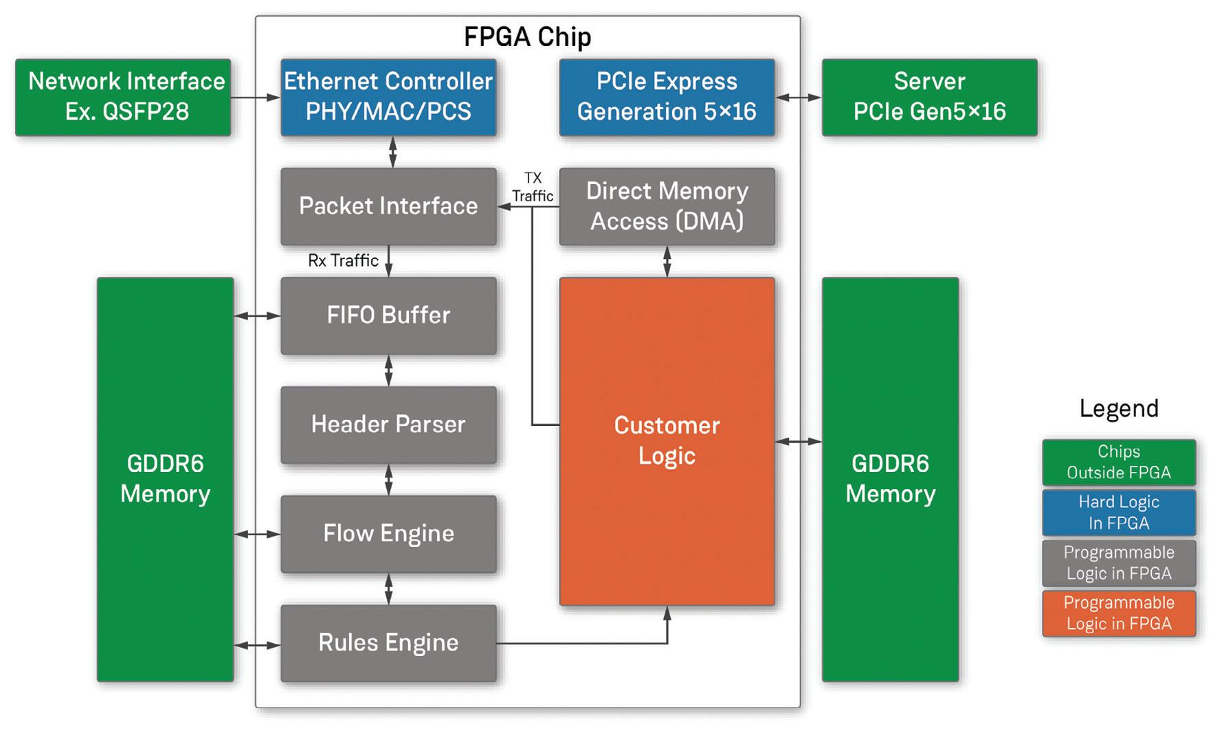
Many newer SmartNICs contain FPGAs, operating as an FPGAbased SmartNIC or an FPGAAugmented SmartNIC. An FPGA-based SmartNIC, shown in Figure 2, is a design that employs the expanded hardware programmability of FPGAs to build any data-plane functions required by the tasks offloaded to the SmartNIC. Because you can program an FPGA, you can tear down and reconfigure the FPGA’s data-plane functions at will and in real-time.
FPGAs can operate at hardware speeds as opposed to being limited by software, often offering several orders of magnitude in performance improvements. The large inherent parallelism in FPGAs leads to SmartNIC designs that exhibit high performance, high bandwidth, and high throughput.
The FPGA-based SmartNIC utilizes both hard logic for basic system input and output functions (blue boxes), as well as programmable soft-logic blocks (box and orange) for advanced packet and network flow processing tasks. A huge region of programmable logic can handle custom functions loaded on demand or written and loaded in the field. These optional logic blocks might include wire-rate packet deduplication within a half-second window, load balancing of packets, and even flows or advanced security functions including unanchored string searches through the entire packet. Such searches might look for potentially thousands of strings in parallel.
FPGA-augmented SmartNICs, on the other hand, are systems that simply add an FPGA to an existing NIC complex. Based on
simply add an FPGA to an existing NIC complex. Based on the design, the NIC can be either an existing multicore SmartNIC or just a simple NIC ASIC. The FPGA can reside either behind or in front of the NIC chip complex or even out-of-band using a secondary PCIe bus.
Overall, SmartNICs that leverage FPGA technology can reap the benefits of good programmability and flexibility, as well as excellent latency and outstanding throughput. However, nothing is free; greater throughput and flexibility means the FPGA often draws more power than similar ASICs, which deliver substantially less performance.

Clearly, you have numerous choices and tradeoffs to balance when it comes to designing a SmartNIC.
Ultimately, a successful SmartNIC design must:
• Implement complex data-plane functions, including multiple match action processing, tunnel termination and origination, traffic metering, and traffic shaping.
• Provide the host processor with per-flow statistics to inform networktuning algorithms that optimize traffic flow.
• Include a high-speed data plane that is programmable through either downloadable logic or code blocks to create a flexible architecture that can easily adapt to changing data plane requirements.


• Work seamlessly with existing data center ecosystems.


To achieve these, it is highly unlikely that any one technology (i.e., ASIC, FPGA, or CPU) will lead to a “passable” SmartNIC. Instead, you should choose at least two technologies such as a combination of ASIC and FPGA. In practice, the best design will likely be one that marries all three design options along with a very high-performance network-on-chip to tie them together.


The SmartNIC, a network interface card with an integrated data processing unit (DPU), is gaining importance for use in data centers. Engineers can design SmartNICs with ASICs, Arm Cores, and/or FPGAs. Design choices come with several tradeoffs. All things considered, a successful SmartNIC design should be programmable, performant, and fit seamlessly within the rest of the system.
References

[1] “Smart NIC Market to Approach $2 Billion by 2027, According to Dell’Oro Group,” Feb. 23, 2023. https://www.delloro.com/news/smartnic-market-to-approach-2-billion-by-2027


[2] Network Interface Card, https://www.sciencedirect.com/topics/ computer-science/network-interface-card
[3] “Émile Baudot Invents the Baudot Code, the First Means of Digital,” Jeremy Norman’s History of Information. https://www. historyofinformation.com/detail.php?id=3058
[4] Christopher Trick, “What is a NIC Card (Network Interface Card)?” Trenton Systems, April 12, 2022. https://www.trentonsystems.com/blog/ nic-card
[5] David Smith, “A Network Engineer’s Perspective of Virtual Extensible LAN (VXLAN),” Connected, December 17, 2018. https:// community.connection.com/network-engineers-perspective-virtualextensible-lan-vxlan/

Engineers have several mmWave over-the-air test methods available for evaluating phased-array antennas used in antenna-in-package designs. Each has pros and cons.
 By Su-Wei Chang, Ethan Lin, Andrew Wu, and Jackrose Kuo, TMYTEK
5G brought mmWave frequencies from 24 GHz to roughly 50 GHz to cellular networks. Those frequencies provide wide bandwidths that enable high data rates. Unfortunately, signals at these frequencies are susceptible to atmospheric absorption, scattering, and blocking. To offset these problems, mmWave depends on phased-array antennas and beam steering to direct energy to the target. Antennain-package (AiP) designs combine antennas with modems and mmWave components. That saves space but eliminates test points, making wired testing impossible. Testing AiP designs require over-the-air (OTA) techniques.
Evaluating antenna characteristics such as gain, phase, and radiation patterns guarantees beam-steering performance through OTA radiation testing is crucial to ensure that these systems meet the required standards for performance, coverage, and reliability.
OTA measurement methods include phased-array, far-field, indirect far-field,
and horn-antenna techniques. Testing
AiP RF front-end systems emphasize the importance of calibrating and measuring gain loss and phase error, which directly affects beamforming performance.
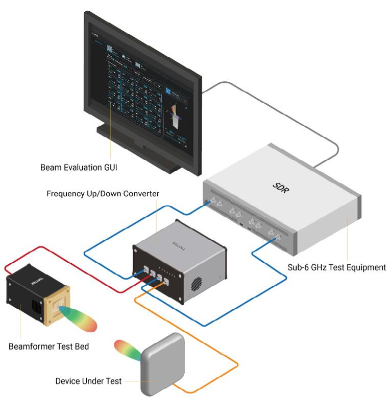
Figure 1 shows an RF front-end module with an integrated antenna array and beamformer ICs that form an active phasedarray beamforming subsystem consisting of:
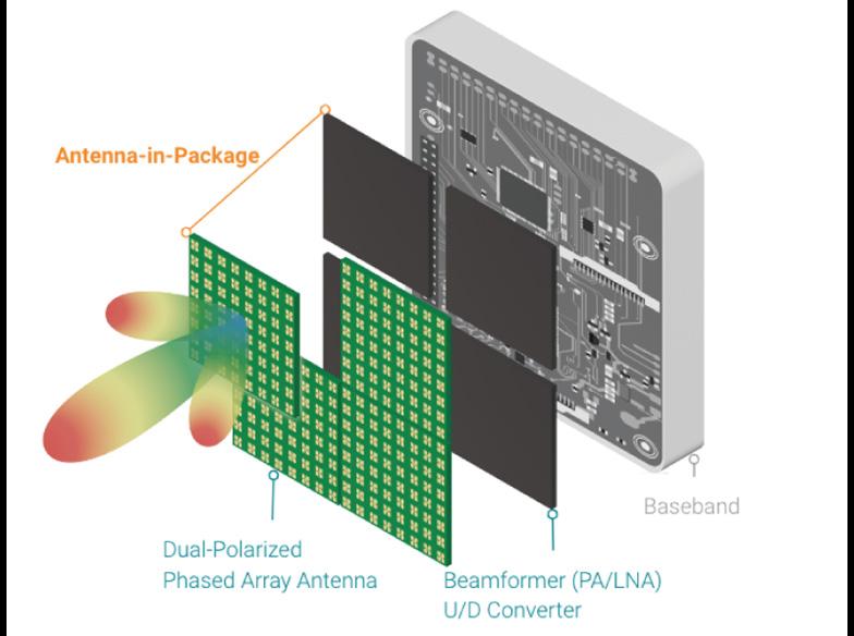
• phase shifters,
• a power amplifier (PA),
• low-noise amplifier (LNA), and
• optional integrated frequency up/down converters, power management, and control.
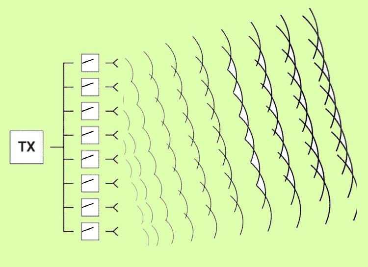
Phased arrays control a signal’s gain and phase, creating constructive and destructive interference that enables beamforming and beam steering, as shown in Figure 2. AiPs are used in 5G/SATCOM applications.
Figure 3 shows a test bed for evaluating beamforming characteristics, algorithms, and other advanced experiments such as MIMO and channel sounding.
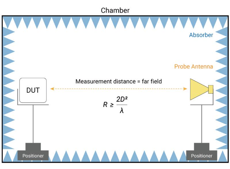
Far-field testing is a commonly used method for 5G mmWave OTA testing. It involves measuring the electromagnetic radiation emitted by the device under test (DUT) at a distance greater than one-tenth of the wavelength of the signal being transmitted; refer to Figure 4. The far-field region is typically defined as the region beyond the Fresnel zone, which is the region surrounding the device where the phase of the electromagnetic waves is not uniform. Far-field testing is typically performed using an anechoic chamber, a specially designed room that absorbs electromagnetic waves to eliminate reflections from the walls and floor. The main advantage
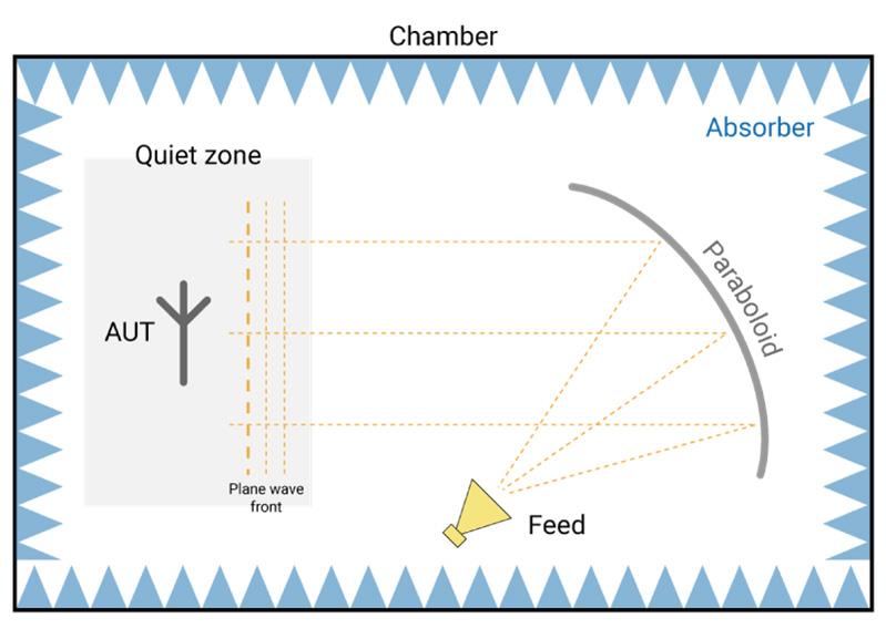
of far-field testing is that it provides a true representation of the antenna’s radiation pattern. Another form of testing called compact antenna test range (CATR) is a type of indirect far-field testing; a measurement method used to evaluate an antenna’s performance in a compact and controlled environment. It involves measuring the electromagnetic radiation emitted by the DUT at a distance greater than one-tenth of the wavelength of the signal being
transmitted but not in the farfield region. See Figure 5 for the environment setup. Indirect far-field testing is typically performed using a reflector or lens to focus the electromagnetic waves emitted by the DUT onto a detector. This method can be less expensive and easier to set up than traditional far-field testing, but it may not be as accurate. CATR is typically used to measure the radiation pattern and gain of an antenna, as well as to evaluate the performance of beamforming algorithms.
Horn-antennas used for testing the radiation pattern of an antenna measures the field strength at the aperture of a horn antenna, as shown in

Figure 6. This method is useful for testing arrays of antennas because the horn can individually illuminate each element of the array. Unfortunately, you need several horn antennas, resulting in increased cabling complexity. The main advantage of horn testing is that it allows for easy isolation of individual elements in an array. Horn testing may not, however, provide as accurate a measurement of far-field radiation pattern representation for the antenna as far-field or indirect farfield testing.
When testing the performance of AiP RF front-end systems, you must
calibrate the test bed and measure gain loss and phase error to ensure that the beamforming performance is up to standard. Gain loss is the difference between the expected and actual gain of an RF system, and likewise, the phase error is the difference between the expected and actual phase of an RF signal. Calibrating and measuring these parameters is crucial to ensure that the beamforming performance of an AiP RF front-end system is consistent and reliable.
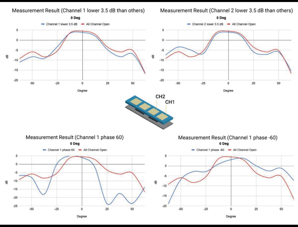
Figure 7 is the experiment of a 1x4 AiP module where the power gain is turned off or turned down, and the phase difference between channels is adjusted. What if it only measures the peak gain (gain at zero degrees)? It would not be able to absolutely justify the difference due to it being under the testing tolerance, which could result in extra troubleshooting effort. Instead of checking and comparing the beam pattern in red (all channels
open for good results) and blue (defect sample), there are clear results that make it easy to identify defects by the beam pattern.
Table 1 compares industry standard measurement methods.
In summary, existing chamberrotator-based measurement solutions provide complete measurement parameters, but they take up significant space and are expensive. In addition, turntable and rotator pattern measurement mechanisms are slow to generate results. Furthermore, although horn testing requires minimal investment for production testing, it evaluates peak only, making it not ideal for identifying defects in phased-array antennas.
As the mmWave market grows and the demand for phasedarray antenna simulation and measurement validation increases, there are various methodologies
• Reliable method for measuring the radiation pattern of an array antenna.
• Most commonly used method for testing array antennas.
• Allows for accurate gain and directivity measurements for the antenna.
• 3D radiation pattern measurements.
Antenna Test Range)
• Allows for testing array antennas in a compact environment.
• Eliminates the need for a large distance between the antenna and test equipment
• 3D radiation pattern measurement.
• Reliable method for measuring the radiation gain of an array antenna.
• Accurate gain and directivity measurements of the antenna when multiple horns are used
• Less expensive solution.
proposed from both academic research and industry in-house experimentation. Note that pattern-based measurements should be crucial to guarantee beamforming performance from a phased-array antenna.
Gain and phase are key factors in beamforming and beam steering. The only test case to guarantee phased-array antenna
• Requires a large distance between the antenna and test equipment, which can be challenging in certain test environments.
• Not well suited for testing array antennas that are close to each other.
• Slow measurement speeds due to mechanical rotator.
• High CAPEX and OPEX.
• Less reliable than direct far-field testing.
• More complex to set up and requires more equipment.
• Slow measurement speed due to mechanical rotator.
• High CAPEX and OPEX.
• Not well suited for testing array antennas that are close to each other.
• Requires a large distance between the antenna and test equipment.
• Only peak gain measurements.
Table
performance is a pattern-based measurement. That means the measurement system should contain multiple detecting probes to detect gain power at specific angles. But how to define resolution versus cost is a design topic based on usage needs.
Because peak gain is detected only by a single horn antenna, what if the system
Market proven measurement method for antenna gain and directivity
× Requires larger testing space and is costly
Alternative measurement method with compact testing space
× Slow measurement speed and is costly
Ultra cost-effective measurement method that is widely produced
× Less testing coverage
incorporates multiple horn antennas and is placed as the sector to detect the gain from different angles? It is thus possible to redraw the gain chart into a “pattern” map. The consequence of horn array methodologies is the beam pattern resolution corresponds to the quantity of horn detection sources. Higher pattern resolutions mean larger horn arrays, which increases cost. When there are many horn detectors in the same measurement system, calibrating each antenna for consistency is also challenging.
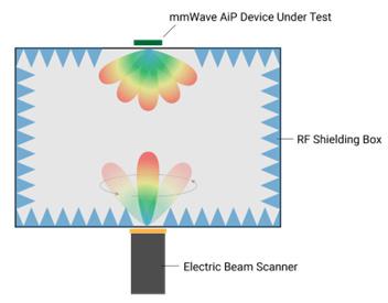
As an alternative to using horn antennas, a well-calibrated AiP system could be used as an electric beam scanner and activate beam-to-beam measurements to detect each beam angle from the DUT. The entire system would ideally be contained inside a chamber box to avoid interference (see Figure 8 for the system concept). Because software controls beam switching and the time delay when switching is mere microseconds, by theory, a full 3D-pattern measurement could be generated within 10 sec. This 3D beampattern measurement methodology is worth continued development and validation.
Measurement space correlates to the frequency and diameter of the antenna, and the only way to minimize space is with near-field testing. The problem: there is no radiation behavior
associated with the near-field region, hence the essential need for NF-FF (near-field to far-field) transformations.
NF-FF calculations should be calibrated and defined in a certain test configuration and chamber environment. Although there are several approaches to transformation equations that result in proven information
mapping, there is ample research and experimentation available for review online, so it will not be discussed here in depth.
To accelerate failure detection, you can use AI software to process large amounts of test data into a characteristic model for pattern recognition. You should analyze beam patterns in real-time to
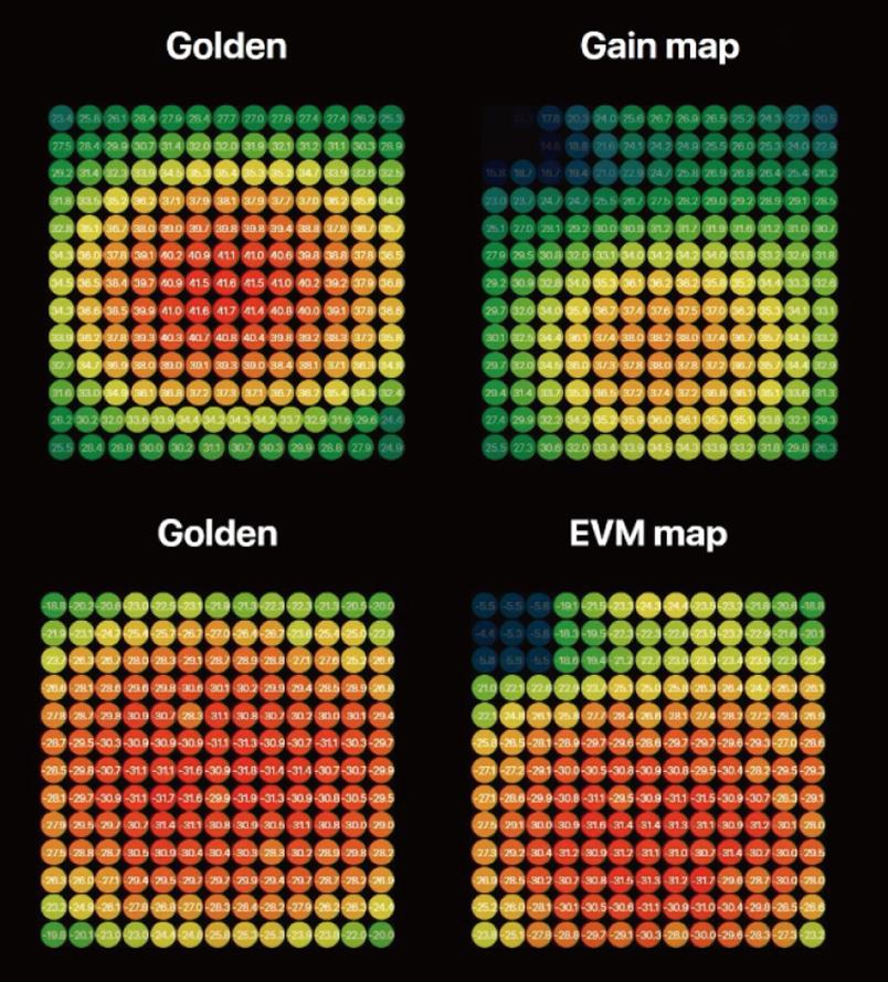
identify failures where defective components could be dispatched using conditional configurations. With such high-speed testing, you can collect measurement results quickly. Doing so lets you build a comprehensive database rich enough to develop AI modeling for advanced intelligent analysis, such as the characteristic comparison of gain and errorvector magnitude (EVM) maps in Figure 9. This approach lets you correlate production batches with characteristics of array elements to significantly improve production efficiency while providing valuable feedback to design engineering teams.
Applying outside-the-box thinking and combining all the above testing methodologies could create a useful OTA testing method that addresses testing speed as well as increases test coverage. As cost is always a key investment consideration, total cost of ownership (TCO) optimization could incorporate a simplified setup with electric scan and AI automation.
5G mmWave OTA testing is an essential process that plays a critical role in the development and deployment of 5G mmWave systems, which operate at frequencies above 24 GHz and offer higher data rates and lower latencies compared to lower frequency bands. OTA testing lets engineers evaluate the performance of mmWave systems under real-world conditions, including the effects of multipath, reflections, and penetration loss. The most important factors are beamforming performance, which is identified by the beam pattern through the gain and phase measurement, and testing speed that launches mmWave from production to commercialization to innovate the marketplace.
A loose connection; a metal roof; power lines. Even a rusty bolt. It’s estimated that mobile operators will spend $1.1 trillion on capital expenditure between 2020 and 2025, much of it allocated to creating, improving, and maintaining its advanced networks — a little corrosion can result in decreased data rates or dropped calls.
Passive intermodulation (PIM) interference is not a new problem for the mobile industry, but it is growing. PIM has become a pressing problem due to the rapid deployment of new technologies, the use of frequency bands located close to each other that are particularly susceptible to this issue, and the increasing number of subscribers. These factors have combined to create a challenging environment where PIM can cause significant disruption and degradation in the performance of wireless networks.
PIM is the generation of interfering signals caused by nonlinearities in a wireless network’s passive components. The interaction of mechanical components — such as loose cables, dirty or corroded connections, or metal-onmetal connections such as fasteners — can produce PIM. When two signals pass through these components, the signals can interfere with each other, creating harmonics that fall directly into the uplink band.
Networks can transmit and receive 4G/5G signals without ever seeing an issue. In busy networks with multiple frequency bands transmitted, however, the chances of causing RF interference increase.
Mobile networks aim to make the best use of the frequencies they license, meaning this is a problem — especially at the crowded lower-band 450 MHz to 1 GHz and mid-spectrum 1 GHz to 6 GHz bands used by many operators for 5G services. Higher frequencies and less crowded networks may be less prone to PIM interference.
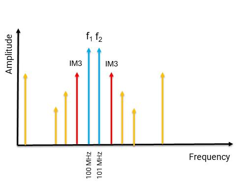
The third harmonic is often the strongest in PIM because it is the result of the second-order nonlinear mixing of two input signals, which generates an intermodulation product at three times the frequency of one of the input signals (see Figure 1 and Table 1). The result is an increase in the noise level affecting desired signals, leading to dropped calls and decreased capacity. To compensate, the power levels of the cellular site will increase so that the signal can be separated from the noise. This spike in power is a big flag to the network that a problem exists, but also creates its own issues.
PIM becomes more apparent when cell sites experience high levels of activity with numerous user devices connected to the network. As the site attempts to overcome the noise and interference within the network, it may need to increase power levels, which can further exacerbate PIM. An example of compensating for noise in a crowded environment
is speaking louder so that the listener can hear your message. In situations where the noise level is high, we naturally adjust our vocal volume to ensure that our message is effectively communicated. Similarly, cell sites trying to overcome noise interference increase their power levels to compensate, which can affect nearby cell sites.
Knowing that an interference problem exists in a network can be straightforward. The previously mentioned increased power use is a big clue, and many networks have fault-detection software that can point to where interference exists. Unfortunately, identifying the sites where PIM interference
5G brought passive intermodulation problems into the spotlight. Now it’s up to engineers and technicians to identify and mitigate signal degradation to minimize dropped calls and other issues.
Danny Sleiman, EXFOFigure 1. Intermodulation (IMD) creates distortion that degrades signal quality, causing PIM. The third harmonic is usually the worst offender.
exists and knowing what is causing the interference at these sites are very different challenges. The origins of PIM interference can be extremely difficult to pinpoint.
First, there are two types of PIM. Internal PIM is caused by the internal RF elements in the infrastructure such as loose connectors, damaged cables and connectors, and faulty elements in the antennas. These issues typically occur between the transmitter and the antenna, and the most common culprit is a damaged or faulty coaxial cable. External PIM is caused by objects located near cell sites. Examples include metallic objects (usually rusty) close to the antenna, metal roofs, or even digital billboards. Interference from either of these domains is difficult to identify.
Dealing with internal PIM can often require a specialist crew climbing a cell tower or accessing a rooftop to look for what might be causing the problem. Those situations entail expense and risk, especially carrying a bulky PIM analyzer. Even then, there’s no guarantee of identifying the problem the first time, so multiple truck rolls may be necessary to find and detect every potential source of PIM. While a corroded coaxial connector is the most likely suspect, this is not guaranteed; the entire process of finding and resolving an internal PIM issue can take weeks to complete. This is due in part to the required analysis, which can be a mostly manual effort rather than using automated technology.
External PIM can be even more difficult to locate. Technicians need to hunt down and pinpoint the source (or sources) causing the interference, and the solution may not be easily apparent. A spectrum analyzer can help pinpoint the source, and the process of interference hunting is highly manual and typically requires RF expertise. In extreme circumstances, the only solution may be to move the site.
Making this bad situation even worse, it’s not immediately obvious when the problem is external or when it is internal. Analysis can mean disconnecting the site from the network for assessment, which is far from ideal for an operator striving to keep customers connected. Technicians have a short window to try and resolve issues so that customers don’t suffer too much disruption.
The nature of PIM interference makes it a particular headache for operators, given that it’s common, hard to pin down, and resolving
it can be expensive. Plus, an extended hunt for PIM interference can cause more problems than it solves. As engineers search for the problem and change connections and hardware, they can end up introducing elements that make the PIM interference worse. Fortunately, there are ways to mitigate these issues.
It may seem counterintuitive in a mobile network that diagnosing PIM issues can involve both fiber and over-the-air RF testing. In fact, by using RF spectrum analysis over the fiber or CPRI protocol, technicians can isolate whether the issue is internal or external PIM. To perform the RF spectrum analysis over the fiber (or CPRI), technicians attach an optical splitter near the baseband unit at the bottom of an antenna tower to diagnose the PIM issue. Performing this analysis from the ground avoids the time and effort of a technician scaling a tower to address interference.
A major benefit is that RF spectrum analysis over the fiber is a passive test application, so the baseband unit and remote radio head will continue to process calls normally, allowing technicians to analyze the uplink spectrum during normal site operation — and during busy periods when PIM is most active.
This type of analysis requires specialist equipment as it must be attuned to different network components — and network equipment from different or multiple vendors means that the encrypted signals along fiber
are not simple to analyze. Processes are available to auto-detect vendors’ proprietary signals, which reduces the configuration by applying intelligence and automation.

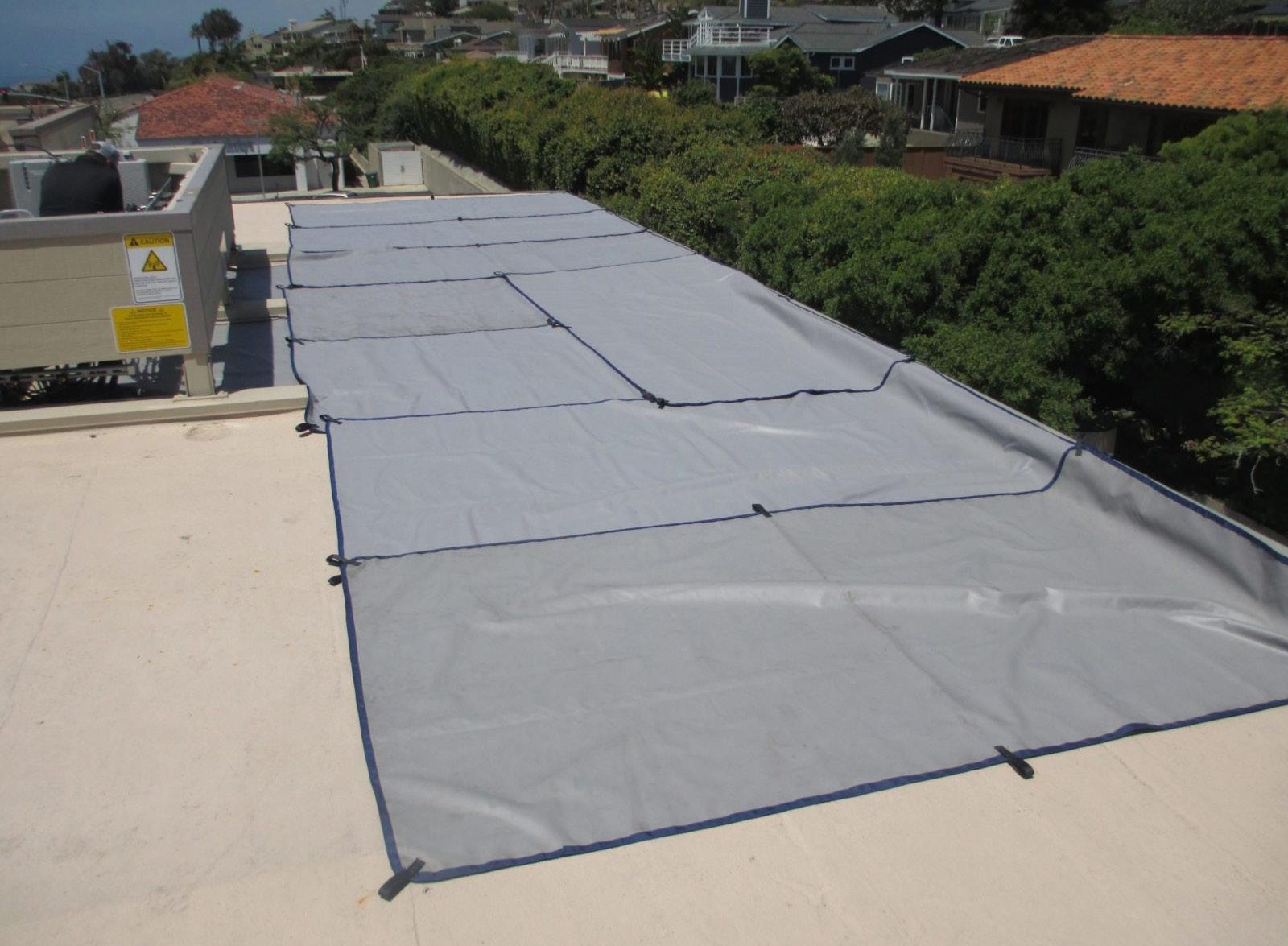
One way to detect if a particular fastener or bolt is causing external PIM interference is to fix or replace it. This isn’t always ideal — if the problem remains then an engineer or technician has spent valuable time and resources repairing something that hasn’t solved the issue. One way around this is quite simple: throw a PIM blanket over the offending item (Figure 2). These suppress the RF signal, meaning it no longer interferes with the site. This way the process of elimination is faster and repairs can be carried out on items that are actually worth fixing.
For situations where the internal or external PIM is not readily diagnosed at a particular site, over-the-air spectrum analyzers with interference hunting connected to a PIM probe or a directional antenna can enable anyone to hunt down the causes of ongoing PIM interference (Figure 3). Many solutions to PIM problems use multiple tools and are too complex to use without advanced expertise, but investing in intelligent equipment means field technicians can detect problems more quickly.
Given that PIM interference causes slower data rates and dropped calls, any customer making regular use of a site is likely to already be suffering from issues. Extended downtime while the problem is located will only make this worse, so ensuring quick resolution is important.
Wherever we have wireless technology, we have PIM because it’s impossible to eliminate entirely. Thus, it’s a consideration that operators need to take seriously. Networks are only going to become more crowded as new technologies increase data throughput and more cell sites are built to cope with demand.
Operators need to approach this with a proactive as well as a reactive approach. The reactive approach will always be necessary, of course. Many sites were built to support older technologies and were upgraded for LTE and now 5G. When these upgrades were in place, problems with PIM became apparent. As PIM is often a result of infrastructure degradation, then dealing with PIM is simply part of ongoing maintenance.
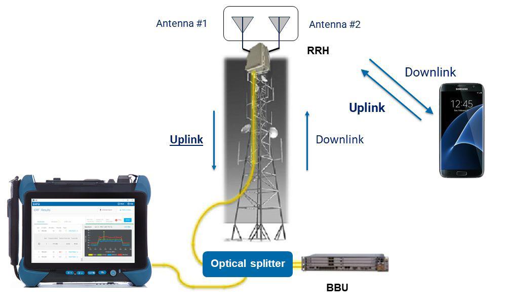
But there are steps that operators can take to prevent PIM issues. As metal-on-metal connections are often a big problem, sites can use plastic fasteners and connections so that these issues don’t arise — stainless steel might be durable, but that doesn’t matter if it’s causing interference. Operators can take other steps to prevent the corrosion of materials. Potential PIM sources can be identified and
mitigated before they become an issue. All network planning, building, and maintenance needs to be carried out with PIM mitigation in mind, not just taking today’s technology into consideration but tomorrow’s as well. The shift to 5G revealed some big
The Women in Engineering Chat Series from Design
World
Register now for past and future WOMEN IN ENGINEERING Webinars

wtwh.me/womenengineering
PIM issues, so what about 6G? Or even further? What about when new bands are made available? Completely future-proofing against PIM interference is impossible, but the negative impact of PIM can be lessened with the right approach.
is a collection of webinars about female engineers who are positively influencing the culture of engineering — as well as design technologies and engineering practices.By Darrin Gile, Microchip Technology
Network elements must meet certain frequency, phase, and time requirements to ensure proper end-to-end network operation. Synchronization architectures defined by the O-RAN alliance dictate how Open RAN equipment can meet these requirements.
Open RAN continues to attract interest from service providers looking to reduce cost, improve competition, and drive technology innovation. The desire for a disaggregated and virtual RAN architecture has introduced more flexibility, competition, and openness to the 5G networks.
The O-RAN Alliance was formed in 2018 to standardize hardware and define open interfaces that ensure interoperability between vendor equipment. Protocols, architectures, and requirements for the control, user, and synchronization planes are defined in O-RAN.WG4.CUS.0-v10.00.
The synchronization plane (S-Plane) addresses network topologies and timing accuracy limits for the fronthaul network connection between the O-RAN radio unit (RU) and distributed unit (DU). The requirements for frequency, phase, and time synchronization follow the 3GPP recommendations and align with the ITU-T network and equipment limits. For time-division duplex (TDD) cellular networks, the base requirement for TDD cellular networks is 3 µsec between base stations, or ±1.5 µsec (G.8271) between the end application and a common point. More stringent accuracy requirements exist for equipment used with advanced radio technologies such as coordinated multipoint or MIMO.
To meet these tighter network limits, equipment will need to meet the Class C (30 nsec) maximum absolute time error defined in G.8372.2.
The S-Plane consists of four topologies for distributing timing through the fronthaul network (RU to DU). These configurations rely on a combination of timebased and frequency-based synchronization techniques. A primary reference time clock (PRTC or ePRTC) located in the network will provide a base time for each network element. The use of GNSS, precision time protocol (PTP), and a physical layer frequency source, most commonly Synchronous Ethernet (SyncE), ensures the RU reliably receives the frequency and, more importantly, the phase and time synchronization
required to operate the network. Figures 1 and 2 show the four defined configurations for supporting network synchronization in the Open RAN fronthaul network.
Configuration LLS-C1
Synchronization for the first configuration occurs through a direct connection between the DU and RU. The DU will receive network time from a precision realtime-clock/telecom grandmaster (PRTC/T-GM) that is either colocated with the DU, or from a remote PRTC/T-GM located further back in the network.


Configuration LLS-C2
For configuration LLS-C2, the DU still receives network time from a co-located PRTC or one further upstream in the network. Network time passes from the DU through
additional switches that reside in the fronthaul network. For best performance, these switches should comprise a fully aware (G.8275.1) network where each node acts as a telecom boundary clock (T-BC). Partially aware networks where one or more switches don’t participate in the filtering of PTP are also allowed. Depending on the type of fronthaul network, the type and number of hops limits the network's overall performance. For example, a fully aware network comprised of Class C (30 nsec) T-BC’s can facilitate more hops than a fullyaware network comprised of Class B (70 nsec) T-BC’s.
Configuration LLS-C3
For the third configuration, both the DU and RU will receive network time from a PRTC located in the fronthaul network.
As with LLS-C2, network time can propagate through the fronthaul network via fully-aware or partially-aware switches. In some cases, the DU may participate as a T-BC in passing time to the RU.
Configuration LLS-C4 is the most preferred and easiest to implement but potentially the costliest of the four topologies. In this configuration, the RU gets time from GNSS as a pulse per second (PPS) clock or from a colocated PRTC/T-GM. The sheer number of 5G NR sites and the location requirements of the GNSS antenna can make this a costly or impractical configuration to deploy. GNSS at the radio sites may also be more susceptible to spoofing or jamming, which can disrupt proper operation.
Like network deployments, the synchronization design of network equipment requires proper planning and design. To satisfy network synchronization limits, equipment will use a combination of timestampers, advanced phase lock loops (PLL), robust software for PTP support, and precision oscillators (Figure 3).
The first key piece of the design is the system synchronizer, which consists of several advanced PLLs. The synchronizer provides jitter and wander filtering for SyncE clocks, input reference-clock monitoring, hitless reference switching, and a numerically controlled oscillator for fine PPS/PTP clock control. The PLLs also provide bandwidths capable of locking directly to PPS clock sources.

Accurate timestampers, PTP software, and an advanced algorithm will manage PTP traffic and provide the tuning calculations needed to accurately track T-GM phase and time. Finally, the precision oscillator is critical to ensure proper holdover and overall performance parameters.
These building blocks are the same for the DU, RU, and any switch participating in timing distribution. The actual implementation of the functional blocks may differ depending on the use case. For example, the precision oscillator may vary depending on the holdover requirements for each network element. A DU needs more stability and must support longer holdover times than an RU. Because of this, RU designs may be able to use higher-end temperature-controlled oscillators (TCXOs) or mini-oven-controlled oscillators (OCXOs) while a DU may use a more expensive OCXO.
You can employ any of several techniques to improve overall time accuracy within a piece of equipment. These techniques range from basic design items such as placing the timestamper as close to the edge of the equipment as possible, to more complex system calibration for phase management within the system. The use of SyncE and more specifically the Enhanced Synchronous Equipment Slave Clock (eEEC), as defined in G.8262.1, provides a stable frequency reference that greatly improves overall phase performance for hybrid configurations.
When using security protocols such as MACsec, take care to ensure that the encryption/decryption adds little or no delay to the timestamping function. Properly design and select the performance of the advanced algorithm and precision oscillator stability to provide the needed performance. For more complex designs, ensuring all timing components involved in the distribution of the PPS clock minimize input-to-output delay variation and outputto-output skew is critical to satisfy even the tightest equipment limits. Some synchronizers take advantage of calibration functionality that provides fine phase control measurements and adjustments. Additional compensation for phase error caused by the temperature and aging of the precision oscillator temperature can also be accomplished. You can use some or all these methods to ensure that equipment meets time and accuracy limits.
Initially, rural and private greenfield networks have been good launching points for deploying Open RAN. As more macro deployments begin to come online, providing high-accuracy network synchronization will be critical for delivering the performance that ultra-low latency applications and advanced radios technologies demand.
5G networks rely on the distribution of packets at high speed between the backhaul network and the air interface. Packets must travel through switches, routers, and networkprocessing units. Reliable packet distribution depends on highly accurate time signals that maintain precise synchronization of network equipment from end to end.
Clocks and oscillators throughout the 5G radio access network (RAN) propagate time signals among network equipment. According to the ITU-T’s recommendations for building a transport network, a timing signal can sustain a maximum error of just ±1.5 µsec in its journey between the backhaul and the radio.
Such a small margin imposes strict demands on the systems and oscillators that maintain stable and accurate timing. At certain points in the network, the strain on these components becomes acute because environmental factors weaken frequency stability. The choice of timing components is also, in some cases, constrained by the host equipment’s physical attributes.
This article offers guidance on choosing the right criteria for evaluating timing components for a 5G RAN, particularly in the critical locations where timing accuracy is most at risk of exceeding its error budget.
5G network technology came in response to market demands for faster downloads, stronger security, more data bandwidth, and connectivity to many more devices, user terminals and IoT nodes. The increasing application of artificial intelligence (AI) in mobile-networked devices, backed by the introduction of multi-access edge computing (MEC), also calls for the lower latency that 5G networks deliver compared to 4G.
Two important features of 5G arise from the use of higher frequencies: the mmWave bands and a shift from frequency-division duplex (FDD) to time-division duplex (TDD) signal modulation. Both changes narrow the margin of error allowed in the timing signals synchronizing 5G payloads and network operations; specifications for jitter and frequency stability must be set much tighter than in the 4G world.
Equipment manufacturers and network operators have learned that timing components have newfound importance in their world; timing has become a fundamental enabler of the new features and capabilities that underpin 5G networks’ revenue models.
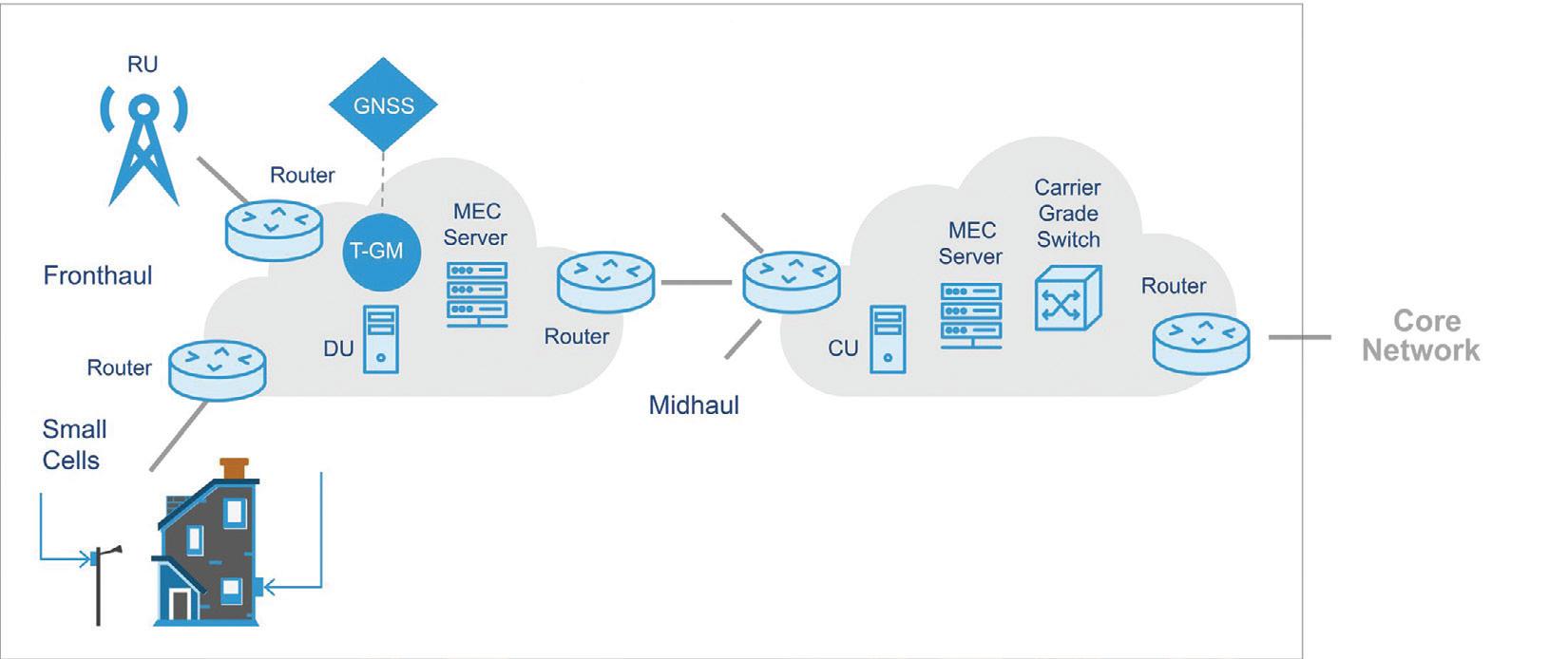
As Figure 1 shows, a packet passes through multiple nodes in a 5G RAN on its journey from the core network to the radio. Data gets routed through the core and RAN, passing through switches and routers. Mid-haul and front-haul networks can employ MEC servers to provide cloud-computing functions, such as AI, close to the end user. This minimizes latency, tightens security, and improves IoT device performance.
5G base stations that employ Open RAN
By Gary Giust, Deepak Tripathi, and Carl Arft, SiTimetechnology have a new structure comprised of three functional units: the central unit (CU), distributed unit (DU), and radio unit (RU). The CU mainly implements non-real-time functions in the higher layers of the protocol stack and can attach to one or more DUs. The DU supports the lower layers of the protocol stack, including part of the physical layer. The RU includes hardware to convert radio signals into a digital stream for transmission over a packet network.
A notable innovation of 5G technology is the proliferation of small cells offering shortrange, high-bandwidth connectivity at the network edge. A small cell may be a femtocell, picocell, or microcell with a range of 10 m, 200 m, or 2000 m, respectively.
Industry standards govern time Synchronization requires a reference for time. In normal operation, this is derived from a Global Navigation Satellite Service (GNSS) radio signal, which is traceable to ultraaccurate atomic clocks running in government laboratories. Distributed throughout the network, this master time signal provides a reliable basis for synchronization.
The methods used to synchronize timing signals that propagate through the network are
5G’s high speeds place extreme demands on the components that maintain accurate time. Compliance with industry timing standards calls for accuracy in the face of temperature changes, shock, and vibration.Figure 1. Equipment in a 5G RAN transports data from a radio unit or small cell to a core network.
governed by industry standards. These standards are typically applied to equipment to make them comply with the 3GPP’s 5G specifications:
• The total end-to-end time error must be less than ±1.5 μs.
• The frequency error at the base-station air interface must be less than ±50 ppb.
• At the Ethernet physical layer, which supports packet transfer in the backhaul and mid-haul networks, Synchronous Ethernet (SyncE) provides frequency synchronization in compliance with the ITU-T G.8262 and G.8262.1 specifications.
Synchronization lets the equipment in a 5G network time-stamp individual packets and downstream equipment to extract reliable time measures from these time stamps. The IEEE 1588 Precision Time Protocol (PTP) provides a standard protocol for time-stamping data in a computer network.
To minimize time error, SyncE may be used to synchronize frequency between items of Ethernet networking equipment and, in combination with PTP, to synchronize the network to the GNSS time signal. For mainstream 5G RAN systems, a combination of PTP and SyncE offers the most accurate way to implement time synchronization. This timing setup, for example, lets equipment operating in ITU-T Class D mode keep time errors to under ±5 ns.
These systems normally depend on the unbroken availability of a GNSS signal to provide a reference time signal. Unfortunately, a CU or DU cannot always get access to upstream GNSS timing. In this case, they must rely on a local oscillator within a telecom grandmaster (T-GM) to maintain timing downstream for proper PTP operation.
When SyncE synchronizes to a reference time signal, timing is handed on from one node to the next. Each piece of network equipment recovers a clock signal from the data passing through it. It cleans the jitter from this recovered clock, then uses this clean clock signal to time data back out onto the line.
This operation repeats down the line, from where the time signal is directly derived from the GNSS clock all the way downstream to the network edge. This recover, clean, and retransmit process ensures that
downstream nodes are frequency synchronized to upstream nodes.
Such frequency synchronization uses jitter attenuators to clean the recovered clock signal. They feature a low-bandwidth phase-locked loop (PLL) operating between 1 mHz and 10 Hz to filter jitter and wander.
This attenuator also benefits from a local oscillator, providing redundancy and fault tolerance using input monitoring and hitless switching. The role of the local oscillator is to maintain an accurate time signal for a limited period if the upstream connection is temporarily lost. This holdover function is particularly important for routers, CUs, and DUs to keep the downstream network running.
The local oscillator’s holdover specification is perhaps the most important parameter for the network equipment designer to evaluate. It sets the period for which the downstream network can continue operating within its specified time-error margin in the absence of a more accurate reference clock. Figure 2 illustrates holdover by showing a local clock’s timing synchronized, or disciplined, to an upstream reference derived from GNSS timing. When this reference is lost, the local clock begins to drift in frequency with a time error, E(th), at a holdover time th.
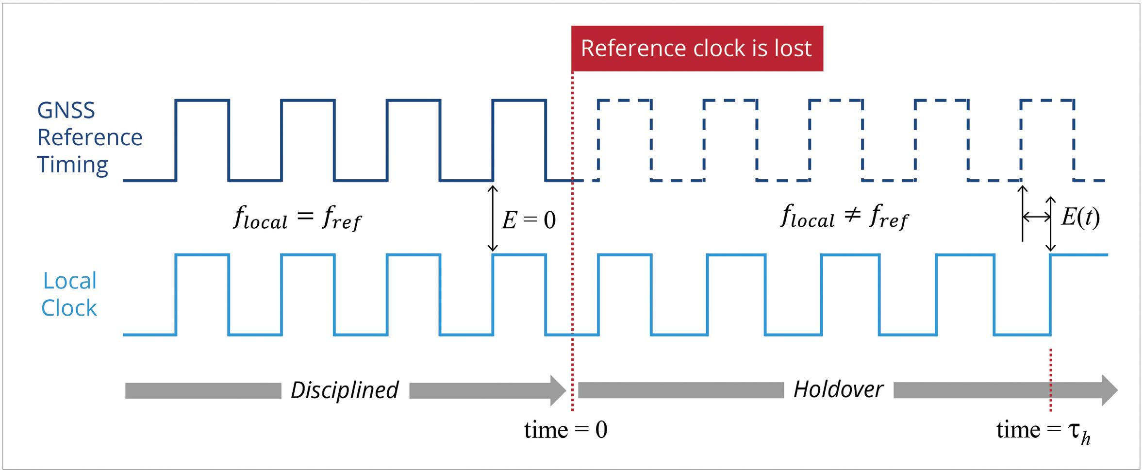
At best, an oven-controlled oscillator (OCXO) typically provides holdover time for between 4 hours and 12 hours, but this type of clock is hot, bulky, and power-hungry. A system that can tolerate a shorter holdover time instead uses temperature-compensated oscillators (TCXOs), which can maintain a holdover from 1 hour to 4 hours.
In the case of CUs and DUs, the nature of the hardware imposes its own constraints. These network elements are transitioning towards using off-the-shelf servers that often embed Open Compute Project (OCP) NIC 3.0 PCIe-based cards. These low-profile cards have limited height to accommodate components, which requires using thin OCXOs, less than 7 mm high, to provide holdover.
PTP packets propagate throughout the network to synchronize its nodes. They might, for example, pass through a telecom boundary clock in the CU or DU and an ordinary clock in the RU.
At each node, a PTP servo disciplines a local oscillator to the time derived from network packets. Because thermal drift is the dominant source of error in the local oscillator, selecting an oscillator with excellent short-term stability is essential. This performance criterion is different from
the measure most often evaluated by electronics system designers, which is frequency stability specified for the lifetime of the device.
A local oscillator will be disciplined regularly, perhaps once a second or even more frequently, making lifetime stability irrelevant. The equipment designer needs to focus on the frequency-over-temperature slope (df/dt)—the steeper the slope over a given temperature rise, the greater the error introduced into the timing signal. Put the other way, oscillators with low df/dt reduce network time error, filtering more packet-delay variation (PDV) by enabling lower PTP servo bandwidths.
Temperature variation is, therefore, a significant cause of timing errors in serverbased network elements such as DUs and CUs. Environmental factors can also disturb timing operations at the network edge. 5G network densification occurs through the installation of small cells in new types of locations including under manhole covers, attached to the sides of buildings, on street lamps, and elsewhere. Unlike the climate-controlled environment of a server room, these locations are exposed to high and low temperature extremes. Most
radios are convection-cooled, so the outside temperature directly affects the temperature inside the enclosure.
This means that radios require local oscillators resilient to changes in temperature and therefore have a low d f/d t. They must also handle temperatures ranging from -20°C to 105°C in a single design for global deployment.
Temperature is not the only environmental stressor affecting local oscillators: shock and vibration can affect radios located close to train or tram lines or busy highways, and storm winds can shake radios mounted in exposed locations, for instance, on streetlight poles. Resistance to shock and vibration is another essential criterion for the evaluation of oscillators in 5G radios.
High-performance timing: the key to 5G’s value 5G networks promise a step-change in throughput, latency, and connectivity compared to 4G. High-speed data interfaces in nodes such as CU and DU servers and switch ICs in routers make this superior performance


possible. Each of these interfaces requires low-jitter clocks or oscillators that offer high immunity to power-supply noise.
Closer to the edge of the network, clocks need to provide high short-term frequency stability over temperature and withstand shock and vibration. 5G network equipment designers will profit from closely studying timing components’ datasheets. Particularly those emphasizing the importance of lowphase jitter, the ability to reject jitter caused by power-supply noise, alongside holdover, low df/dt, and excellent resistance to shock and vibration.
Demands for bandwidth-intensive, data-driven services are fueling a rise in compute, data storage, and networking capabilities. These rises put pressure on connectors and cable to deliver data at higher speeds with better signals and less heat.
Whether it’s 5G implementations, our growing reliance on AI and machine learning, or the soaring impact of the Internet of Things, data centers must constantly adapt.
To keep pace, companies are moving from monolithic data center designs to distributed, disaggregated architectures.
This modularized approach avoids the extensive investment of traditional server or storage buildouts. Instead, mix-and-match components are used to upgrade capabilities—cutting the time, effort, and expense to deploy new hardware.
But the effectiveness of this approach depends upon meeting networking and compute connectivity requirements. Specifically, there are four keys for optimization in the data center via modularization: space constraints, signal integrity, cabling, and thermal management.
Two trends have converged in recent years to put a squeeze on data centers. The first is shrinking square footage. To minimize their carbon footprint and lower energy bills, property costs, and site maintenance, companies for the past decade have been building smaller data centers.
The second is hardware density. Despite greater use of the cloud and virtualization, more hardware is being crammed into data
centers than ever. In a 2020 survey by AFCOM, 68% of respondents said rack density has increased over the past three years, and 26% said the increase was significant [1].
Some of this is due to the growth of AI, which requires the use of more specialized chips, but it is also part of a broader trend of disaggregation and modularization. Disaggregation takes the traditional all-inone server and decomposes it into separate resources, such as separate hardware for compute, memory, storage, and networking. Disaggregation also takes the form of edge computing, where computing power moves away from the cloud, getting closer to the user.
In many cases, these resources remain within the same rack unit, but are broken out onto separate modules. While this approach retains the same basic architecture as a monolithic design, it complicates connectivity. Components that once lived on the same PCB now reside on different modules. As such, they can no longer communicate via PCB traces. Instead, modules must communicate via connectors and cables.
This raises the question of how to fit more connectors and cables into less space. To deal with this concern, several new types of connectors have been developed.

Mezzanine connectors, which let two PCBs couple together, are a good example (Figure 1). These connectors help when adding accelerators to CPU cards. In fact, the Open Compute Project’s Open Accelerator
By Liz Hardin, MolexInfrastructure (OAI) group has developed specifications for an open-hardware compute accelerator module form factor and its interconnects. Mezzanine connectors based on the OAI Universal Baseboard (UBB) Design Specification v1.5 112G can achieve twice the bandwidth of the prior generation while maintaining an extremely small footprint. Edge cards offer a similar solution, enabling you to add memory, storage, and accessory cards to a system in a highly spaceefficient manner (Figure 2). As with mezzanine connectors, edge cards are available in standardized configurations recognized by JEDEC, Open Compute Project, and Gen-Z Consortium. This enables large-volume purchases for a variety of applications, aiding not only space efficiency but also cost efficiency.
Just as disaggregation complicates volumetric efficiency, it also introduces new concerns around signal integrity. This was already an area of concern as PCBs are currently managing 5 GHz signals at best. New functionality requirements for applications such as 5G are driving signals of 25 GHz and higher. Modularization only adds to the challenge by increasing the number of components that must communicate over relatively long distances over lossy PCB traces. Consequently, highspeed, high-density applications are moving away from traditional board designs to allow for intra-module cable connections.
New PCIe connectors can create a direct, height-optimized connection from anywhere in the system to near an ASIC. That lets signals bypass board traces and systems use lower loss materials. The result is not only more spaceefficient wiring, but better signal integrity, lower insertion loss, and reduced latency.
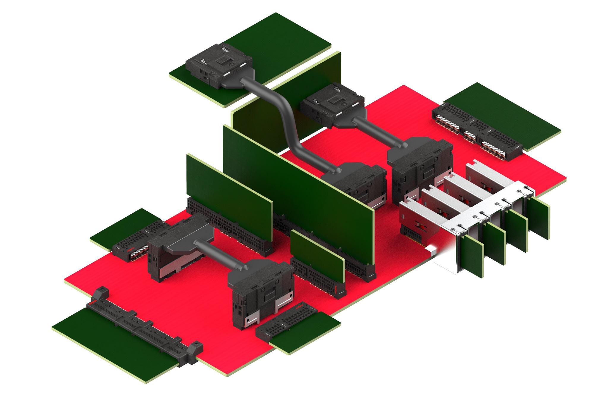
The latest PCIe gen 4 and 5 cabling and connector systems can provide high bandwidth in server and storage applications up to 32 Gb/sec (Figure 3). Some of these connectors are also ideal for SAS protocols. Not only do they support current SAS-3 standards, but they are future-proofed for SAS-4 (24 Gb/sec). Use of this new generation of connectors should help solve data center space issues and boost performance in download systems well into the future.
Increasing data rates also create complications for front panels. Here again a new generation of interconnect systems plays a key role. These cable and connector assemblies can deliver 400 Gb/ sec per port with outstanding signal integrity—all in a widely

accepted, high-density pluggable form factor. The result is minimized tray and panel space coupled with maximized performance.
Thus far we have focused on the issues within a given rack unit. Modularization means that in many cases, functions that were once housed within a single server are now spread across multiple boxes, creating a greater need for cabling to connect subsystems. Deciding which type of cable to
use requires balancing individual data center needs with cost and energy considerations.
Passive cables, including direct-attach copper cables (DACs), have been a standard in rack architecture for decades. With transmissions of 56 Gb/ sec PAM4, DACs can connect the top-of-rack (TOR) switch to all the servers on the rack within a space of up to 2.0 m to 3.0 m without excessive signal loss. For data centers operating at these lower frequencies, they are a good option that saves on energy and cable costs.
But as data centers move up to 112 Gb/sec PAM4, DACs used in distances beyond 2.0 m can
experience unacceptable losses. They may become unable to transmit a clear signal long enough to connect the TOR with servers located lower on the rack, leading data center managers to consider other alternatives.
Active electrical cables (AECs) provide a middle-ground option that effectively span lengths of up to 7.0 m for plug-and-play upgrades. As a result, data centers are installing AECs, which include re-timers at each end. They clean and recondition the signal, amplifying it and removing the noise as it comes in and again as it exits, providing fast transmission and near-zero data loss throughout the journey.
Though AECs do use power, their small diameter helps improve airflow from the front through the back of servers — an important benefit for thermal management. It also makes installing cable bundles easier and faster.
For high-performance computing and longer reach, you can’t beat active fiber optic cable (AOC), which uses electricalto-optical conversion on the cable ends to improve speed and distance performance while remaining compatible with other common electrical interfaces.
With a transmission reach of
100 m to 300 m, AOCs can link switches, servers, and storage between different racks inside the data center, or even for data center-to-data center connections. DACs may still connect switches, servers, and storage within racks.
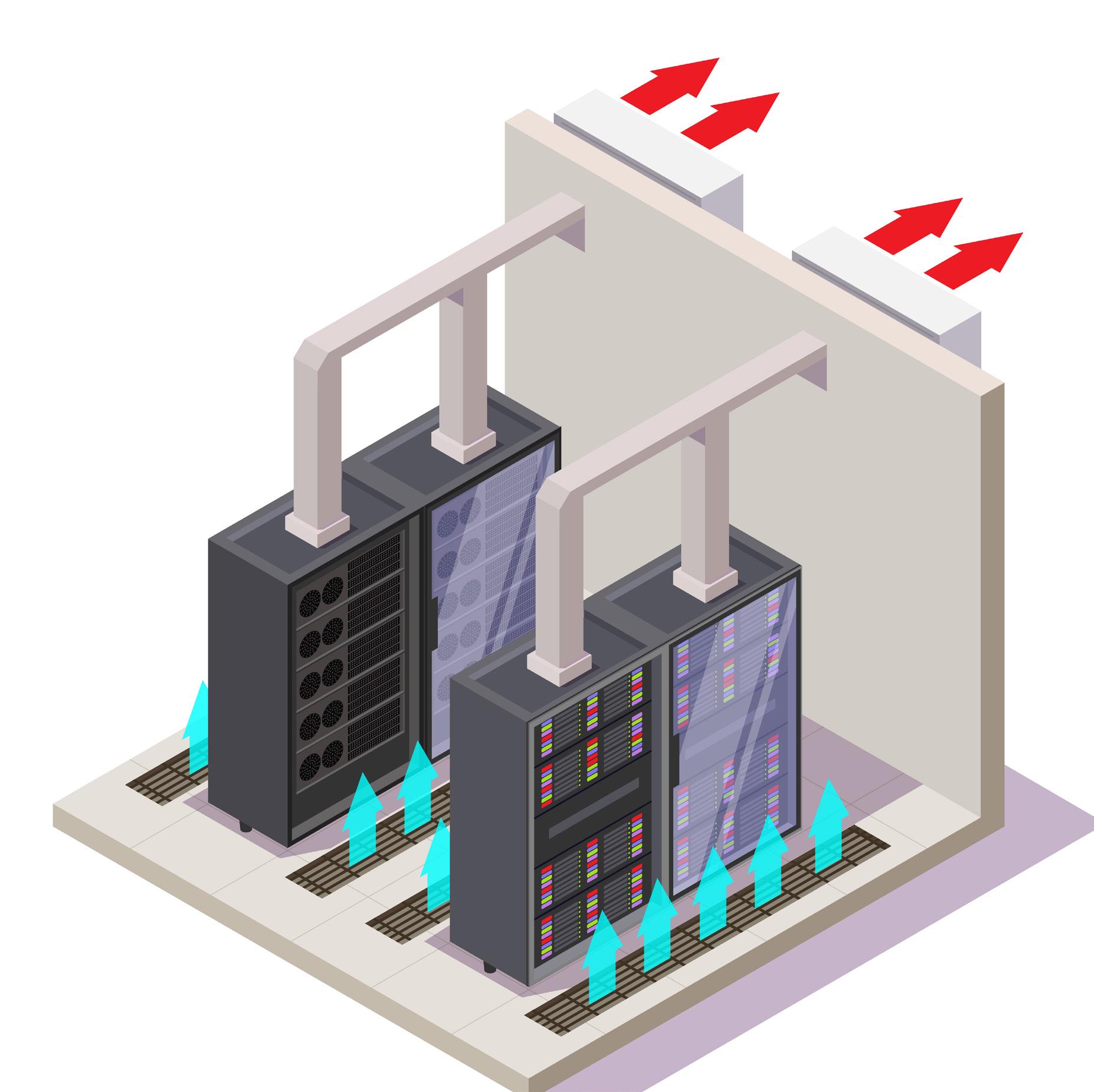
AOC’s weigh just a quarter of copper with half the bulk, which lets it dissipate heat better. Because it can’t conduct electric current, it isn’t vulnerable to electromagnetic interference.
Of course, AOC is not a universal, one-size-fits-all cable technology. Different configurations can peacefully co-exist, giving data centers the flexibility to adapt as technology change accelerates.
The increases in hardware density, data throughput, and cabling complexity are all contributing to difficulties in thermal management. Several cooling techniques have been used over the past decades, ranging from advanced heatsinks to full immersion liquid cooling. Each system has its advantages and challenges.
Fans are the oldest and simplest cooling method, sitting in the back of an equipment enclosure and pushing or pulling air through and away from it (Figure 4). Unfortunately, as engineers pack ever more computing functions into chips, these chips require larger and larger heatsinks. Given the space constraints of the data center, cooling with fans alone is becoming an increasingly untenable option.
A liquid-cooling system may be installed to replace fans or used in combination with them. In this system, a coolant liquid is piped in. As the liquid travels along the pipe at the base of components, it gathers some of the heat being generated and carries it to a heat exchanger, a metal cold plate that replaces the heatsink of a fan. The heat exchanger transfers the heat out of the system and the liquid repeats its cooling circuit.
Conductive liquid cooling is more efficient than fans, but it is complicated to install and difficult to maintain.
In immersion cooling, an entire device or machine is submerged into a bath of non-conductive, cooled liquid, which transfers heat away from it without requiring fans. Immersion is by far the most effective method of carrying heat away from equipment. Because it is more efficient, it can lower the data center’s carbon footprint by an estimated 15% to 30%. In the current
environment of high energy costs and ambitious sustainability goals, immersion cooling is gaining popularity. Managing it is, however, extremely complex, and this has limited the scope of its adoption.
Bring the four keys into harmony
While we have discussed space constraints, signal integrity, cabling, and thermal management as largely separate topics, these four keys to data center optimization are of course tightly interrelated. Tight space constraints and increased cabling both have the potential to restrict airflow, which makes thermal management more challenging. Thus, there is an increasing need for careful consideration of these interdependent factors before a single rack is placed. Careful thermal simulations that account for all heat sources and airflow pathways can avoid problems during deployment.
[1] Andy Patrizio, “Data centers are shrinking but not going away,” Network World, May 5, 2020. https://www.networkworld.com/ article/3541296/data-centers-are-shrinkingbut-not-going-away.html
Circuit-protection components such as fuses and TVS diodes protect power and data circuits from damage. Here’s where and how to insert them into your circuits.
The next generation of cellular communications, the 5G network, will help the IoT reach its full potential. IoT includes many devices and physical objects such as home appliances, vehicles, and “smart” cities.
IoT connectivity depends on the advancements of the 5G network compared to the current 4G LTE networks. The download speed of up to 1 Gbps for 5G, up to ten times faster than 4G, and lower latency, allows for swift file transfers. 5G networks also offer greater capacity to handle more traffic and greater consistency, which can unlock economic and societal opportunities.
With those opportunities comes the need for increased investment in supporting infrastructure. This need includes small-cell and macro cell base stations, with the small cells located on rooftops or light poles to transmit mmWave signals starting at 24 GHz. Millimeter waves can travel only a short distance and can be blocked or disrupted by walls, windows, and even weather. Macro cells generally operate via an antenna mounted on a traditional tower, which is subject to hazards that can affect the reliability and lifetime of the equipment. Engineers must protect circuits and systems from:
• Transient voltage surges resulting from large inductive load switching caused by motors,
• Current overloads,
• Electrostatic discharge (ESD), and
• Short circuits.
As a design engineer, you can add protection to this 5G infrastructure by creating circuits to protect against electrical hazards.
Begin with a detailed description of a macro base station and recommendations for protecting the base station circuitry. Two crucial focus areas are the tower-mounted amplifier and the advanced antenna systems.
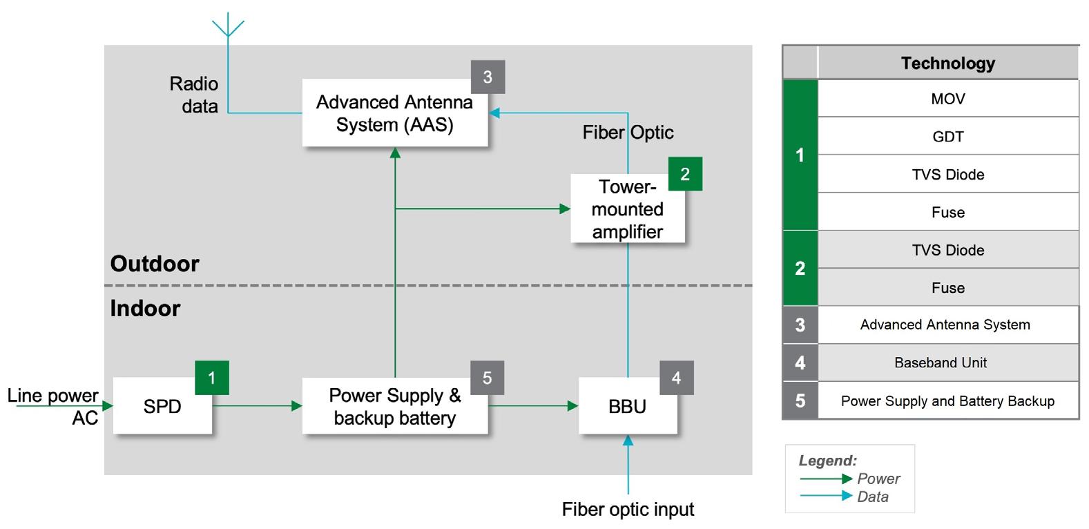
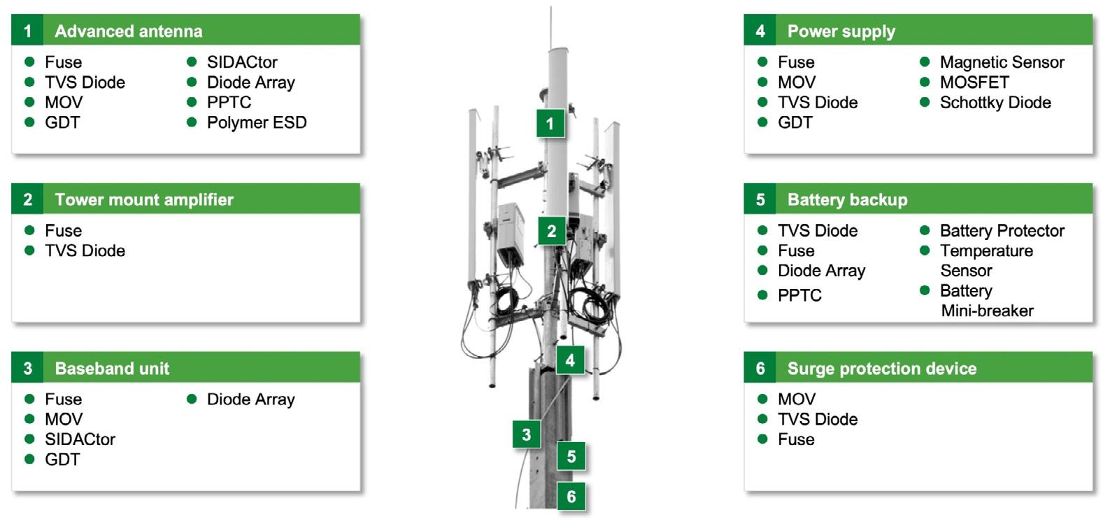
The base station connects to individual mobile phones and other wireless tools such as tablets, smartwatches, and IoT devices through a core network. The base station is a fixed transceiver that acts as the primary transmission and reception communication hub for wireless devices. The base station modulates baseband information and transmits it to mobile devices. Base stations also receive mobile device transmissions, modulate them, and send them to the wireline infrastructure.
Macro base stations reside on towers ranging in height from 50 ft. to 200 ft. These are highly visible structures and strategically located to maximize coverage within a defined geographic area. The base station connects to all wireless devices attempting communication within that geographic or coverage area.
A 5G base station will include advanced, active antenna systems populated by numerous
antennas in multiple input-multiple output (MIMO) configurations. These antennas provide:
• Faster data transmission rates,
• Higher transmission and reception capacity, and
• More efficient delivery of RF power.
Figure 1 details the elements that comprise a base station and lists the recommended protection, control, and sensing components to protect and to improve the base station circuit efficiency.
Figure 2 shows a base station circuit block diagram.
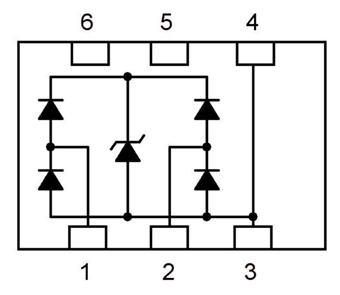
The AC power line interfaces with the surge protection device (SPD). As a result, the SPD is also subject to all the transients that can impact the AC power line. In this situation, the best option is a surgesuppression fuse on the input of the surge-protection circuit. These fuses can withstand lightning surges up to 200 kA based on transient surges defined in UL 1449 Surge Protective Devices, UL 1449 and IEC 610004-5. Under short-circuit conditions, this fuse also provides currentlimiting protection.
As further protection to absorb a lightning strike or other large transients provoked by load changes on the power line, consider using a series
combination of a metal oxide varistor (MOV) and gas discharge tube (GDT). Place the combined MOV-GDT as close to the entrance of the AC line on the circuit as possible to minimize transient propagation into the circuit. Also, connect the MOV between Line and Neutral and connect the GDT from Neutral to Ground. As an alternative to an MOV, in certain circumstances, a high-power transient voltage suppressor (TVS) diode can suffice. The maximum surge-handling capacity of the TVS diode is adequate for the AC power line feed as it has faster response times and it can clamp transients at lower voltages.
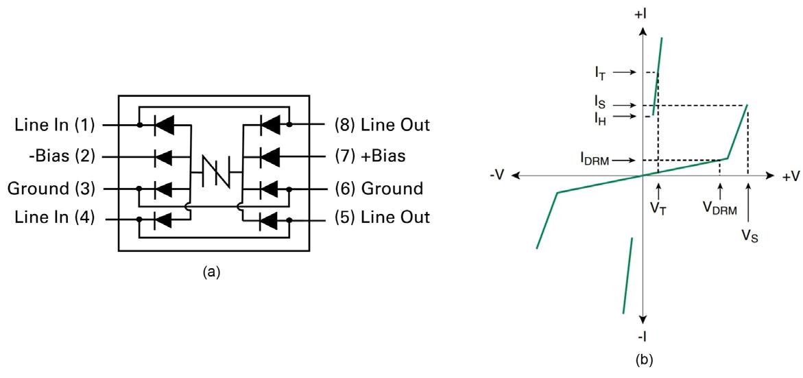
An Advanced Antenna System (AAS) receives and transmits information, audio, and data communications from and to mobile wireless devices within a defined geographic range. See the circuit block diagram for an AAS in Figure 3. The digital packets from the Baseband Unit (BBU) are converted to analog data, then upconverted for RF transmission. Any RF signals received are down-converted and digitized for transmission to the BBU.
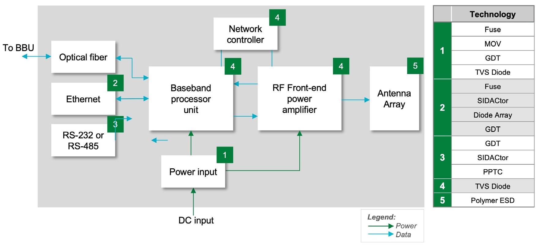
Anything exposed to the outdoors, such as tower-mounted amplifiers, is prone to lightning strikes and
You can establish transient protection with crowbar protection components to protect the integrity of communication ports. Figure 4 shows a protection thyristor, which protects two data lines from ESD strikes when a Power-overEthernet (PoE) communication link is in play. Another option is a TVS diode array along with a gas discharge tube.
ESD. A series fuse and a parallel TVS diode can work to protect against current overloads and absorb lightning or ESD transient strikes. A surface-mount TVS diode package can help overcome space constraints while safely absorbing current overloads as high as 10 kA.
The power-input circuit provides DC power for the other AAS circuits. A best practice for this DC circuit would be a fast-acting fuse for overcurrent protection. Use surface-mount, fast-acting versions to save space. Consider an MOV and GDT in series as an additional option to protect the front end of the power-input circuit from transients that have passed through the SPD and the power supply and backup-battery circuit.
TVS diode at the Power Input circuit’s back end can also supply protection. TVS diodes have a lower clamping voltage than MOVs, which enables the use of lower-voltage-rated and lower-cost components in the downstream circuits.
Figure 5 shows an example of a two-line TVS diode array that employs a Zener diode for clamping a transient, rather than a protection thyristor, which crowbars the transient. Consider using low-capacitance versions of these components to minimize the impact on the quality of the data transmissions. When the protocol is PoE, include a fuse to protect the Ethernet circuit from any overload from crossed lines connecting to the circuit.
For RS-232 and RS-485 interfaces, consider using a protection thyristor and a gas discharge tube (GDT) combination for transient protection. A resettable polymeric positive temperature coefficient fuse provides increased design flexibility when seeking crossed-line and current overload protection.
Baseband processor unit, network controller, and RF
front-end power amplifier
Use a TVS diode to provide transient and ESD protection for these three circuits. Versions of TVS diodes can absorb up to 30 kV from an ESD strike. Also, versions are available in uni-directional or bi-directional formats in surface mount packaging.
Antenna Array
A polymer ESD suppression device, designed to absorb fast-rising ESD transients up to magnitudes of 30 kV, can help protect components such as the antenna array, which is directly exposed to atmospheric conditions. These devices have extremely low capacitance to minimize loading on the antenna that can distort transmitted and received signals. Versions of polymer ESD suppressors can have capacitances on the order of 0.09 pF and lower values.
Baseband Unit

The BBU links the AAS and the wireline infrastructure, encoding transmissions and decoding received signals while processing data from calls and transmissions. The same components recommended for the AAS power-input unit will supply the same protection for this circuit. A straightforward method is to copy the protection scheme used
for the AAS Ethernet circuit on the BBU’s Ethernet circuit. Figure 6 illustrates the BBU and its dedicated power supply.
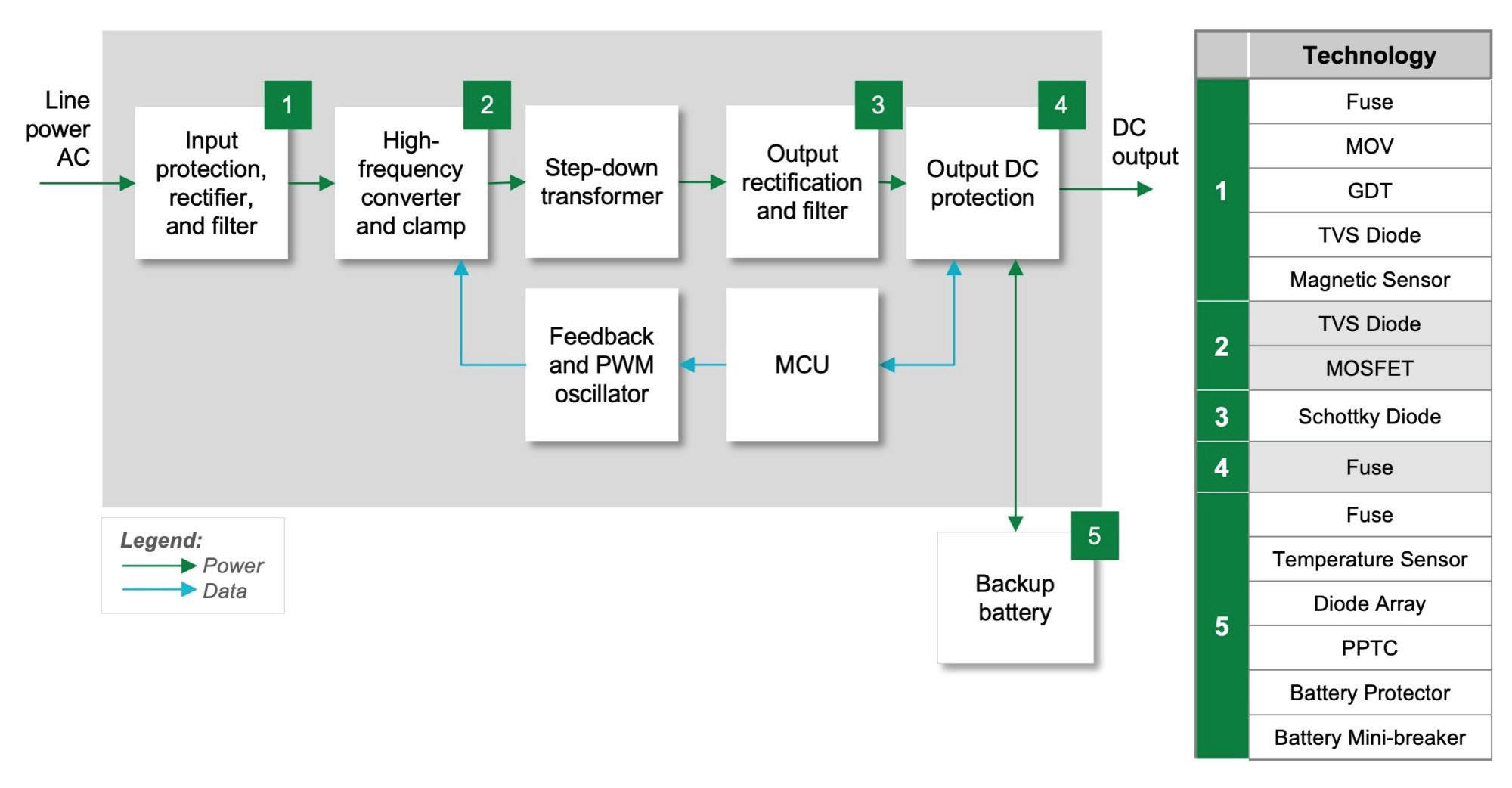
HDMI interface data lines should also have ESD protection. Consider using a 4-line TVS diode array, as shown in Figure 7, to absorb ESD strikes up to 20 kV. Look for TVS diode arrays that have low leakage currents (below 50 nA) and low capacitance (under 0.5 pF) to minimize disturbance for
high-speed HDMI transmissions. Consider voltage transient protection for the DSP, the critical block in the BBU. As with other circuits in the AAS, consider a TVS diode to provide unidirectional or bidirectional ESD protection up to 30 kV.
When AC line power is down or disabled, attain AC line power and DC battery backup from the power supply and backup battery System. Figure 8 shows the circuit blocks of these systems.
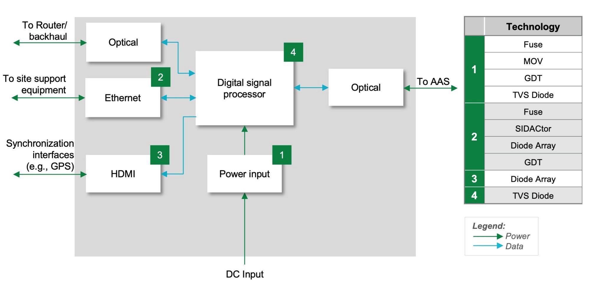
The input protection, rectifier, and filter circuit (block 1 in Figure
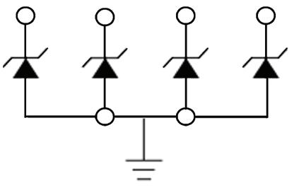
8) convert the AC input to DC. Due to its interface with the AC line, it needs the full suite of overcurrent and overvoltage transient protection. For current overload and short circuit protection, consider:
• Use a fast-acting fuse to prevent damage to the power semiconductors in the power supply.
• Be sure that the fuse selected has a current rating to avoid nuisance failures due to the power supply’s inrush current,
• Confirm the fuse’s voltage rating exceeds the voltage on the AC line.
As with the other power-supply circuits, incorporate an MOV-GDT combination across the input line to absorb AC line-induced voltage transients and protect the circuit. Try a TVS diode in the circuit to increase immunity to transient surges and improve long-term reliability. Finally, consider adding a magnetic sensor into the circuit to ensure that the power supply is turned off when the electronics enclosure door is opened. The high-frequency converter and clamp circuit (block 2) convert the rectified AC line voltage into a pulsed waveform in the kilohertz frequency range. Use a TVS diode
to absorb any transients that passed through the input circuitry and protect the downstream circuitry. Try a MOSFET with low RDS(ON) and high dV/dt to maximize the switching power supply’s efficiency and reduce on-state power consumption and switching power losses.
The output rectification and filter circuit (block 3) converts the pulsed voltage back to DC. Use Schottky diode rectifiers with ultra-low forward voltage to reduce losses in the circuit. Improve supply efficiency with a low forward voltage drop, Schottky diode.
Utilize a fast-acting fuse in the output DC protection circuit (block 4) to protect the power supply from any overload failures in the loads, including the AAS and the Baseband Unit.
A backup battery (block 5) is one of the best ways to support the base station when AC power is interrupted. Support the base station by:
• Providing a fast-acting fuse on the battery circuit for overload protection.


• Monitoring battery temperature rise to ensure battery safety.

• Placing surface mount thermistors on the battery pack modules.
• Protecting the battery pack modules from overcharging.
A three-terminal device could replace a fast-acting fuse to detect an overvoltage condition and disconnect the modules from the charging voltage.
A mini-breaker, which can be a switch paralleled with a polymer-positive temperature coefficient, can back up the circuit’s battery management IC. This component provides the battery pack with overtemperature and overcurrent protection, preventing the battery pack from entering either an over-charge or under-discharge condition.
The battery management system in the backup battery circuit has voltagesense lines connecting to each battery pack’s individual cells. These sense lines are susceptible to ESD and other voltage transients. Use TVS diode arrays consisting of a package with two TVS diodes connected anode-to-anode on the sense lines for bipolar transient protection.
When the backup battery circuit uses the I2C communication protocol to transmit the status of the battery pack from the fuel gauge IC to the battery management IC, consider utilizing a polymer positive temperature coefficient component for limiting current on the I2C lines during a high
voltage transient. This series component protects the overvoltage components that safely absorb transients on the I2C data lines.


Communication infrastructure must have extremely high reliability so uptime can exceed 99.9%. Using the recommended component technologies will help provide the high reliability needed for wireless communication infrastructure by protecting the circuitry from the five sources of electrical hazards. The low cost of the components outweighs the high cost of a base station failure and the disruption to communication.
Protect your reputation as a reliable 5G equipment supplier and gain a competitive advantage by protecting the base station from overload current and voltage transient hazards.


Sub-terahertz communications for 6G will become a reality only after engineers achieve a solid understanding of electromagnetic wave propagation in the as-yet insufficiently researched frequencies above 100 GHz. After achieving that knowledge, we can then derive channel models to enable systemlevel simulations of the new standard. Channel models for 4G and 5G cannot simply be extended above 100 GHz; engineers must verify and finetune knowledge to correctly reflect the impact of the environment for various use cases. We must, for example, understand outdoor scenarios and indoor industrial scenarios where human bodies, vehicles, and environmental conditions such as rain strongly influence signal propagation.
5G pioneered the use of millimeter wave frequencies with bandwidths up to 400 MHz per component carrier to enable transmission rates necessary for
By Taro Eichler,demanding real-time applications such as wireless factory automation. 6G technology is aiming at significantly higher transmission rates and lower latencies. Large contiguous frequency ranges for ultra-high data rates with bandwidths of several GHz are only available above 100 GHz.
From channel sounding to channel models
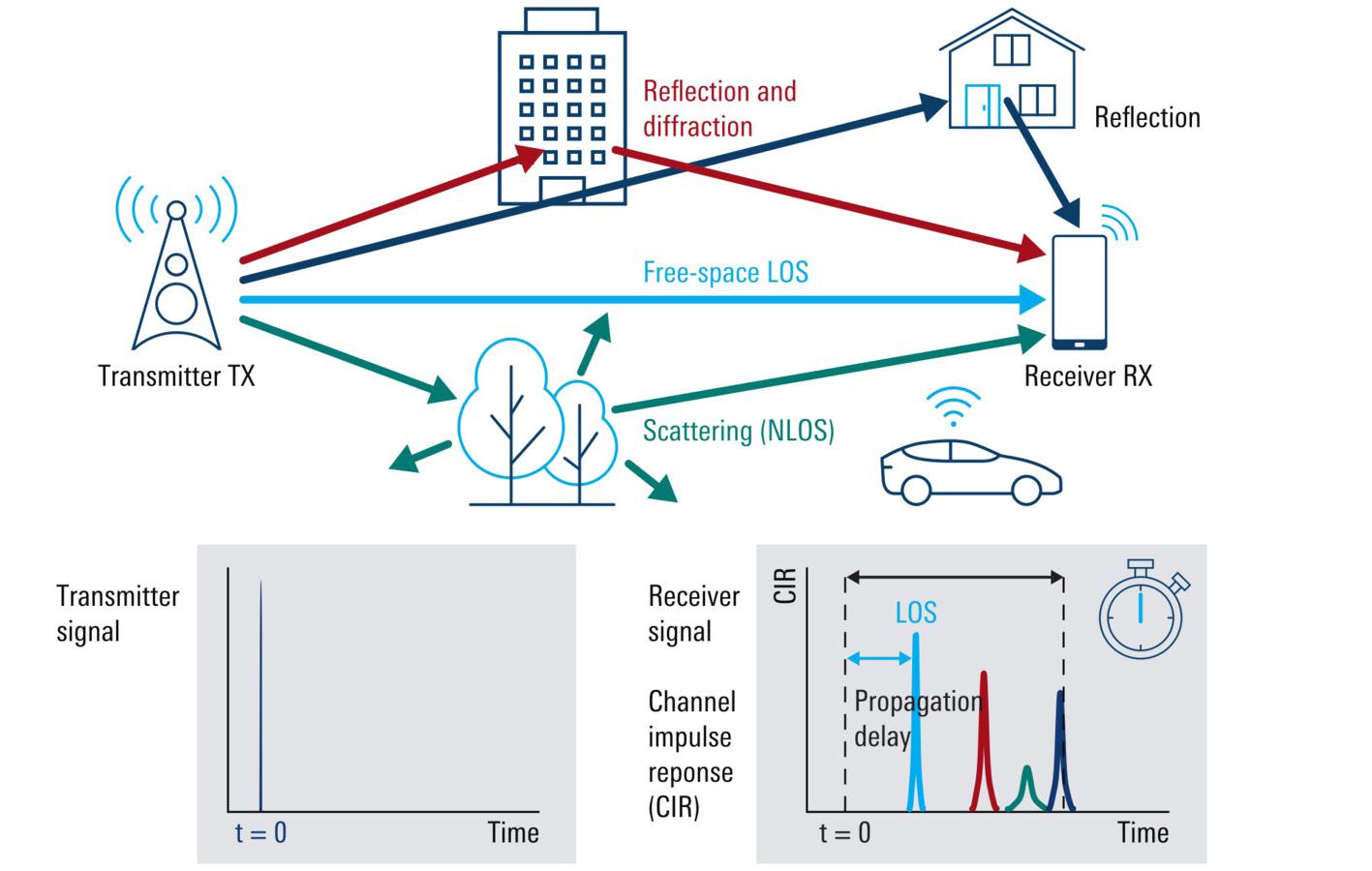
Channel measurements by channel sounding deliver an image of the propagation properties of electromagnetic waves at a particular frequency. The term “channel sounding” comes from sonar technology, where a ship or submarine sends short acoustic pulses and records the reflections in the time domain. This provides a viable image of the surroundings.
With sonar, the transmitter and receiver are in the same place. As for channel sounding of electromagnetic waves, the transmitter and receiver are spatially separated. In time domain channel sounding, a modulated pulse signal with excellent autocorrelation properties, such as a Frank-ZadoffChu (FZC) sequence, serves as a “ping” whose
Efforts to explore and “unlock” this frequency region require an interdisciplinary approach with high-frequency RF semiconductor technology. The THz region also shows great promise for many application areas ranging from imaging to spectroscopy to sensing.
Rohde & Schwarz
channel impulse response (CIR) is recorded [1]. This propagationtime measurement is very similar to the time-delay measurements performed in a GPS receiver in reference to the GPS satellites (and subsequently inferring the position information), where each satellite transmits its specific correlation sequence.
The CIR includes both the direct propagation components (line of sight, LOS) and all reflection and scattering components (non-lineof-sight, NLOS) from objects in the environment (Figure 1). We can derive channel-model parameters and their values from the results.
Objects are only “physically visible” to electromagnetic waves and function as reflectors or scatterers when they are at least as large as the wavelength of the incident wave. This means that at a frequency of 30 GHz, objects with dimensions in the centimeter range already act as reflectors.
Earlier channel-sounding projects include a high-resolution channel measurement campaign at 67 GHz on a Tokyo street canyon [2]. To support the 3GPP efforts, Rohde & Schwarz collaborated with the Fraunhofer Heinrich Hertz Institute (HHI) to perform measurements in its Memmingen and Teisnach production plants, not only in the 28 GHz and 66 GHz millimeter wave frequency bands, but also in the 3.7 GHz to 3.8 GHz band designated for private campus networks in Germany [3]. Channel measurements in the Memmingen production plant have very recently been extended to frequencies in the D-band (110 GHz to 170 GHz).
For 6G, the focus is on channels at frequencies beyond 100 GHz. In a collaborative effort with the Fraunhofer HHI and the Fraunhofer Institute for Applied Solid State Physics (IAF), we developed a research setup that performs signal generation
and analysis at frequencies from 275 GHz to 325 GHz with a bandwidth of 2 GHz. The signal can be used to perform channel measurements and is modulated with novel waveforms for transmission experiments.
Several semiconductor technologies have proved relevant for mmWave applications, so 6G testing combines various semiconductor technologies to optimize performance and energy consumption. Applicable technologies include combinations of InP (speed), CMOS (integration density), and GaN (output power). In particular, InGaAs mHEMT MMICs provide for extremely lownoise and broadband applications at room temperature.
The first results for outdoor scenarios and for an indoor conference room were followed by a more systematic study of the channel propagation characteristics at sub-THz frequencies (158 GHz and 300 GHz) conducted on the campus of the Rohde & Schwarz headquarters in Munich. The study focused on two representative scenarios: a “street canyon” (urban micro-cellular UMi) scenario in a corridor between two R&D buildings [4], and an indoor measurement campaign in an atrium similar to a shopping mall or airport concourse [5].

For a “street canyon” scenario, the stationary transmitter (Tx) was placed at a height of 1.5 m using a bicycle stand. From there, the scenery leads into a more open space with a small plaza and isolated trees (Figure 2).
We mounted the receiver (Rx) and test equipment on a wireless platform (camera dolly) at a height of 1.5 m. We positioned it at various distances from the transmitter up to 170 m. Most of the measurements were in line-of-sight. Example measurements show the CIR for aligned antennas at 30 m for 158
GHz and 300 GHz. The first peak with a delay (time of flight) of 0.1 µs represents the LOS path, corresponding to 30 m. Multipath components are also visible and more pronounced at 158 GHz than at 300 GHz. Path loss exponent can be derived from this set of largescale measurements. We found multipath components at larger delays over nearly the complete measurement set. CIRs were measured at 158 GHz with aligned antennas over a distance from 10 m to 170 m.
Further evaluation of the measured data sets involved analyzing the angular information. At each measurement point, the receiver was rotated to 24 equally spaced angular positions, resulting in spatial scanning of the radio channel in the azimuth plane with 15° resolution.
Based on this estimation of paths, we can calculate the overall received power (i.e. effective overall path gain) from all paths. Although the channel at 300 GHz is much sparser than at 158 GHz, results show clearly that there is
little difference in overall power. Additional paths at 158 GHz could be resolved owing to the high sensitivity of the measurement principle, but they do not significantly contribute to overall power. Furthermore, statistical parameters such as the root mean square (RMS) delay spread, and the RMS angular spread can be evaluated from these results.
Further results for the channel-measurement campaign were performed in an urban micro-cellular (UMi) street canyon scenario at 158 GHz and 300 GHz.
We performed indoor measurements in a building’s large open space, which acted as a shopping mall/airport scenario. The hall is around 52 m × 13 m with a ceiling height of around 20 m. The Tx antenna was configured at a fixed position in front of the elevators at the building entrance at a height of 1.5 m, whilst the receiver was mounted on a wireless platform (antenna height 1.5 m) and moved to distinct positions on a rectangular grid covering the complete floor area.
Estimated paths, position 4, 158 GHz
We measured angle-resolved estimated paths with the LOS peak and several multipath components (Figure 3). Indoor measurements at 158 GHz with a 40 m distance demonstrate the presence of multipath components from different directions, contributing to higher overall received power compared to the outdoor measurements (–71.4 dB at 40 m vs. –75.1 dB at 30 m).
Another interesting representation of the results can be visualized using a rose plot where each “pie” represents the overall power in the respective angle bin, normalized to overall power (Figure 4). Single contributions from distinct paths within one angle bin are depicted by dots. This clearly shows that just one or two angle bins account for almost all the overall power and that within one bin, only a few paths contribute significantly. Although the test equipment received most of the power in the LOS direction, significant multipaths arrive from all measured azimuth directions.
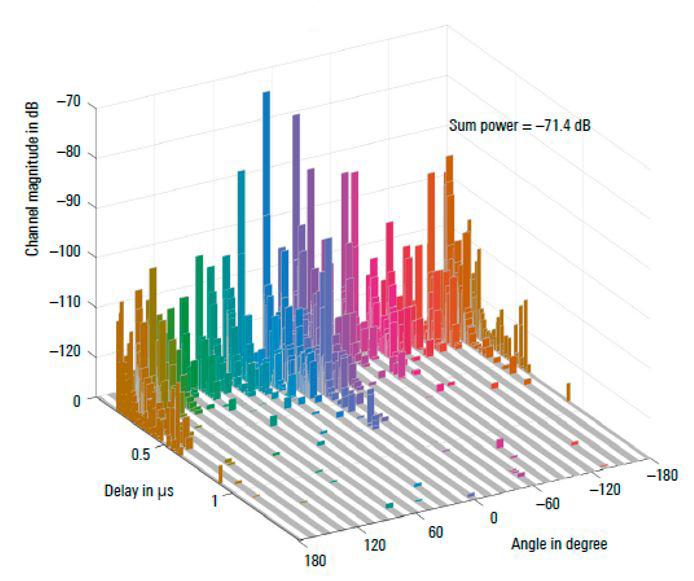
We then extended the frequency range to 300 GHz and analyzed angle-resolved channel-impulse responses with regards to channel parameters such as delay and angular spread. The analysis shows, with a decreasing Rx antenna directivity and an increasing SNR, the number of multipath components increases rapidly [6].
We also performed a study in the same environment at 160 GHz with a bandwidth of 4 GHz. The analysis of these extensive indoor directional channel measurements shows that with the abundance of spectrum in the sub-THz space and thus very high bandwidths, very simple modulation schemes (i.e. single-carrier) and equalization techniques can be used while still achieving significant capacity gains. [7]
The first results of these channel-sounding measurement campaigns have contributed to the ITU-R Working Party 5D (W5PD) report on “Technical feasibility of IMT in bands above 100 GHz” with the objective to study and provide information on the technical feasibility of mobile cellular technologies in bands above 92 GHz (IMT meaning International Mobile Telecommunications standards). The report will be consulted at the International Telecommunication Union (ITU) World Radio Conference 2023, where we expect additional frequency bands beyond 100 GHz to be discussed and considered for allocation at the subsequent WRC27. The current 3GPP channel model is only validated up to 100 GHz. A crucial first step for the standardization process for 6G is to extend this channel model to higher frequencies. Future research will continue to provide insight into the fundamentals of channel propagation above 100 GHz with a focus on 6G communications.
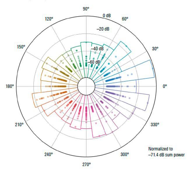
[1] D. Chu, “Polyphase codes with good periodic correlation properties (Corresp.),” in IEEE Transactions on Information Theory, vol. 18, no. 4, pp. 531-532, July 1972, doi: 10.1109/TIT.1972.1054840
[2] M. Peter, W. Keusgen, T. Eichler, K. Yanagisawa, K. Kitao, T. Imai, M. Inomata, Y. Okumura and T. Nakamura, “High-Resolution
Estimated paths, position 4, 158 GHz
Directional Channel Measurements at 67 GHz and Advanced Analysis of Interactions Using Geometric Information,” 2018 IEEE International Symposium on Antennas and Propagation & USNC/URSI National Radio Science Meeting, pp. 77 to 78, 2018.
[3] M. Schmieder, T. Eichler, S. Wittig, M. Peter and W. Keusgen, “Measurement and Characterization of an Indoor Industrial Environment at 3.7 and 28 GHz,” 2020 14th European Conference on Antennas and Propagation (EuCAP), Copenhagen, Denmark, 2020, pp. 1-5, doi: 10.23919/ EuCAP48036.2020.9135943.
[4] W. Keusgen, A. Schultze, M. Peter and T. Eichler, “Sub-THz Channel Measurements at 158 GHz and 300 GHz in a Street Canyon Environment,” in submitted to 2022 Joint European Conference on Networks and Communications & 6G Summit (EuCNC/6G Summit), https://arxiv.org/abs/2203.04404, Grenoble, 2022.
[5] A. Schultze, W. Keusgen, M. Peter and T. Eichler, “Observations on the Angular Statistics of the Indoor Sub-THz Radio Channel at 158 GHz,” 2022 IEEE USNC-URSI Radio Science Meeting (Joint with AP-S Symposium), Denver, CO, USA, 2022, pp. 9-10, doi: 10.23919/ USNC-URSI52669.2022.9887443.
[6] Alper Schultze, Ramez Askar, Michael Peter, Wilhelm Keusgen, Taro Eichler, “Angle-Resolved THz Channel Measurements at 300 GHz in a Shopping Mall Scenario,” 17th European Conference on Antennas and Propagation (EuCAP 2023), Florence, Italy, 2023.
[7] accepted for IEEE Communications Magazine (March 2023 issue), Channel Modeling and Signal Processing for Terahertz Communications, Lorenzo Miretti, Thomas Kühne, Alper Schultze, Wilhelm Keusgen, Giuseppe Caire, Michael Peter, Sławomir Sta´nczak, and Taro Eichler, “Little or No Equalization Is Needed in Energy-Efficient SubTHz Mobile Access.”
The high level of integration in today’s mmWave phone means traditional test methods no longer apply.
By David Vondran and Rodrigo Carrillo-Ramirez, Teradyne5G, the first cellular generation to use the mmWave spectrum, can deliver faster data rates (up to 10x better than LTE). 5G can accommodate more simultaneous subscribers with higher reliability services. These improvements make 5G ideal for specific deployments such as dense urban environments — airports, stadiums, and metropolitan areas.
mmWave smartphones contain highly integrated components. Unlike at lower frequencies, test systems can no longer perform conducted tests at all manufacturing steps. While testing at the wafer level can use techniques found at sub-6 GHz frequencies, mmWave components such as antenna-in-package (AiP) must use over-the-air (OTA) test procedures.
In the US, network operators have procured mmWave bands and deployed mmWave networks. Table 1 outlines the four primary mmWave bands (i.e., 24 GHz, 28 GHz, 39 GHz, and 47 GHz) by carrier.
According to a mobile data traffic outlook report from Ericsson [1], the typical US subscriber in 2028 will consume 55 GB monthly. Why so much compared to today’s roughly 15 GB averages? This predicted traffic growth comes from estimates for extended reality-type services (XR) — augmented reality (AR), virtual reality (VR), and mixed reality (MR). On top of that, increased and higher-resolution video traffic, currently about 70% of all data traffic, will also contribute to this growth.
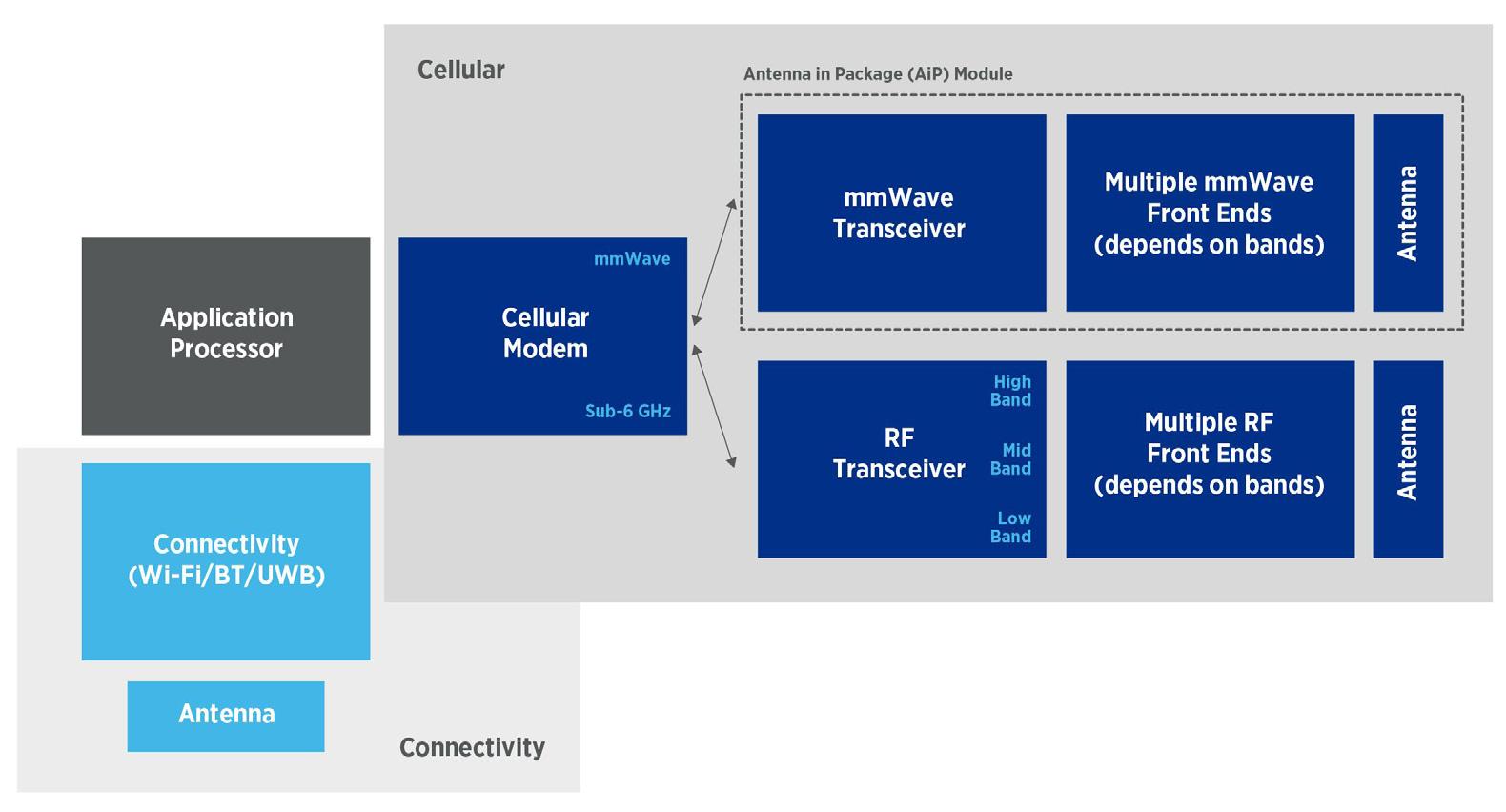
mmWave hasn’t yet seen the accelerated
growth that typically accompanies new connectivity technologies. The data-traffic outlooks indicate that it won’t be long before congestion and hunger for throughput open the floodgates. The initial generation of mmWavecapable devices will help develop the mmWave ecosystem, which includes manufacturing tests.
While the US has allocated 39 GHz and 47 GHz for cellular use, the 26 GHz to 28 GHz mmWave band seems poised to become the standard for global coverage. Therefore, we expect the target market for mmWave will soon become ten times larger, measured in billions of subscribers.
Forward-looking manufacturers have risen to meet this emerging demand. Since 2019, more than 400 5G mmWave capable mobile devices have come to market, which indicates that mmWave is catching on. Table 2 breaks down these device capabilities according to their supported mmWave bands.
Now that we’ve seen things from the network operators’ perspective, these smartphones are worth a closer look to understand the other half of the wireless equation.
The functional block diagram in Figure 1 shows how 5G smartphones organize the intricate constellation of components to enable wireless communication between subscribers and network operators. The application processor, which controls all smartphone operations, joins everything. In general, the connectivity bands are served by separate RF signal paths for unlicensed band operations such as in the 2.4 GHz, 5 GHz, and 6 GHz bands. Similarly, separate RF and mmWave paths serve licensedband operations for the cellular bands.
Think of each wireless signal path as consisting of a modem, transceiver, and path to an antenna(s), which could include other RF front-end components such as switches, tuners, and multiplexers. In this organized manner, the wireless signal paths between the application processor and the antennas become pathways from RF to bits. And these paths establish the wireless links that deliver wireless services for the subscriber.
Focusing on the cellular path, the modem is the hub for the wireless cellular linkages. Furthermore, the RF transceiver handles all the sub-6 GHz activities for data transmission and reception. Likewise, the mmWave transceiver handles all mmWave data transmission and reception. The actual number of wireless bands depends on the network operator’s plan to deliver services to their subscribers.
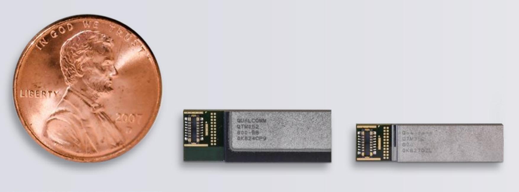
The RF transceiver must support all operational bands for the network operator. Within the transceiver are separate transmit and receive paths for each band. The total number of bands depends on a network operator’s spread across 1G/2G/3G/4G/5G and could total as many as 70 bands. Additionally, antenna technology has evolved to accommodate massive input, massive output (MIMO) features that simultaneously transmit and receive on four antennas. Thus, the transceiver must perform consistently at high levels and across all supported bands. This vital functionality, flexibility, and reliability rest on remarkable integration and complexity that needs testing.
Like the RF transceiver, the mmWave transceiver must also
support all of a network operator’s operational bands. In the mmWave spectrum, these bands are the 24 GHz, 28 GHz, 39 GHz, and eventually, 47 GHz bands. Given that mmWave communication involves shorter wavelengths relative to sub-6 GHz, its signal paths are also smaller. In fact, the semiconductor ecosystem seems to have standardized on an antenna in package (AiP) module to combine the mmWave transceiver, power management IC (PMIC), beamformer, and antenna array into a single modular package. Figure 2
also shows how additional band support has an inevitable ripple effect as all the signal paths must align to support the wireless link.
We can now see how the application processor, cellular modem, and transceivers have become integrated, complex semiconductor devices. Even this virtual tear-down risks oversimplification. Many of these devices have separate PMICs that regulate their power to improve
modem, transceiver, RF front end, and antenna. Every successive generation of these devices has ripple effects in the advanced packaging necessary to achieve higher performance and more complex integration. Automated test equipment (ATE) satisfies the production need for quality.
Test workflow for highvolume manufacture of Sub-6 GHz components has become ubiquitous. Test engineers attempt to eliminate defects as early in the production process as possible. As a rule of thumb, defects get ten times more expensive to capture at each successive production step. The wafer test insertion uses ATE to separate good and bad die.
illustrates this miniaturization trend by showing AiP modules, where the most modern is at right. This makes the AiP module easy to integrate into a signal path but makes testing them more difficult.
As Table 3 summarizes, AiP has undergone four generations so far. The current AiP modules support multiple mmWave bands. This achievement has accelerated mmWave technology adoption. It
battery life. They also contain custom antennas that streamline the signal paths to the base station with highly optimized signal-tonoise ratios to achieve faster and more reliable data rates.
As we’ve seen, the main functional blocks of a 5G smartphone include the application processor,
These tests are usually DC or low frequency in nature (not RF). This first test insertion, termed wafer sort, is designed to eliminate as many defects as possible. As a result, this step typically has the lowest yield.
Next, package-level test also uses ATE to ensure operation and performance that meets statistical expectations to avoid shipping defects and outliers. These RF tests consist of both CW and modulated signals and can include calibration procedures. This insertion is designed to typically have a much better yield than the wafer test.
Lastly, the RF chip integrates into a module (or system assembly) to finalize the RF signal chain and fulfill its mission in the smartphone architecture, including antenna connection(s). In this production step, the module undergoes one last system-level test (SLT) insertion for a conducted test (not over the
air), including possible calibration procedures. This insertion typically provides the highest possible yield.
This workflow ensures quality and consistency throughout the supply chain for the RF signal chain, whether this package serves a singular function or offers integrated capabilities. Note that mmWave test coverage is the sum of two insertions and variations on the test strategy are possible depending on the root cause of defect mechanisms. The manufacturing goal is defect-free shipments. In practice, the quality metric describing the final SLT output is measured by defective parts per million (DPPM).
This Sub-6 GHz workflow also represents the best practices to follow for manufacturing the AiP module in the mmWave signal chain.
Advanced packaging in the AiP module enables miniaturization within the 5G smartphone. It also imposes challenges on the manufacturing process, which must adapt to the complexity and integration of the mmWave signal chain into this single package. As we compare the RF and mmWave signal chains, two main differences summarize these mmWave test challenges for AiP modules.
In the interest of miniaturization, the AiP module doesn’t employ the same traditional packaging techniques employed in the previously described RF workflow. Instead, advanced packaging to integrate die with substrate and antenna array introduces new challenges to finding defects related to the elimination of packaging elements to achieve miniaturization.
Given the small wavelengths in mmWave, close coupling between the transceiver and antenna array (via a substrate) offers superior wireless performance compared to using separate, discrete elements. This tight coupling eliminates excessive transmission loss. Unfortunately, it also eliminates conventional test points and best practices for the conducted test. A new test method that measures differences between antenna array — over the air (OTA) and available conducted test interface at 5G-IF — is necessary for calibration and defect detection.
Compared to the RF best practices, the mmWave workflow illustration in Figure 3 shows the new emerging simplification and complexity in testing AiP modules.

Test workflow for high-volume manufacture of mmWave components has yet to become as ubiquitous as with RF. Indeed, it’s still evolving with every new generation of AiP modules. Like RF, test engineers attempt
to eliminate defects as early in the production process as possible.
As with sub-6 GHz, wafer-test insertion uses ATE to separate good and bad die. These tests employ wafer probes and test with both electrical and mmWave signals. This first test insertion, termed wafer sort, eliminates as many defects as possible and, as with the RF test, typically has the lowest yield. The output is a known good die (KGD).
Lastly, the KGD integrates into the AiP module to finalize the mmWave signal chain. In this production step, the module is placed in an optimal anechoic chamber that is handlerfriendly and undergoes one last system-level test (SLT) insertion using OTA methods, including possible calibration procedures using both CW and modulated signals. This insertion is designed to typically provide the highest possible yield.
Like the RF signal chain, this workflow ensures quality and consistency in the mmWave signal chain. Note that test coverage is the sum of all three insertions and variations on the test strategy are possible depending on the root cause of defect mechanisms.
With so many variables and technologies at play, testing the RF-to-bits components inside a 5G smartphone is no small task. Any test strategy for 5G smartphones must account for higher frequency, greater bandwidth, increased site density, and enhanced performance while also maintaining automated test equipment (ATE) expectations for modularity and versatility. This requires expertise in many disciplines to succeed, especially when that test leaves no room for manual intervention. If successful, however, it can fuel innovation, quality, and profitability by meeting manufacturing volumes and lowering test cost.
[1] Mobile data traffic outlook, Ericsson, 2022. https://www.ericsson.com/en/reports-andpapers/mobility-report/dataforecasts/mobiletraffic-forecast
If you perform an internet search on “what is 6G?”, you’ll surely see sustainability. The number of companies with goals to be carbon neutral grows daily. In many ways, major players in the wireless industry lead the charge. There is a recognition our collective industry actions can not only reduce the carbon footprint of our business, but we are also responsible for creating the tools other industries need to reduce their carbon footprint. For the first time, the idea of building networks and devices for sustainability is at the center of design conversations instead of being thought of as an optimization challenge, fixed after deployment.
Wireless systems and networks consume large amounts of resources to operate today, from electricity to raw materials. The power required to run networks is, for example, massive. In 2020, approximately 201 terawatt hours (TWh)
of energy was consumed in China to power its mobile networks. This number equates to roughly 2.3% of the total energy consumption of the entire country [1]. Given the current pace of 5G network deployment and consumer demand, the energy usage of wireless networks in China is expected to grow 289% between 2020 and 2035 according to a recent study by Greenpeace [2]. To meet the electricity needs of this growth rate, future networks must be more energy efficient. The radio access network (RAN) is an obvious first place to start. Why?
GSMA Intelligence published a report looking at the energy efficiency in current networks [3]. It shows that the RAN consumes 73% of the energy used by network operators. It should, however, not be the only area taken into consideration. Figure 1 shows the dramatic increase in energy used by data centers in 5G versus 4G and this trend should continue. The decentralization and virtualization of the RAN being popularized through Open RAN initiatives will continue to push processing traditionally done in the RAN into software-based distribution units (DUs) and centralized units (CUs).
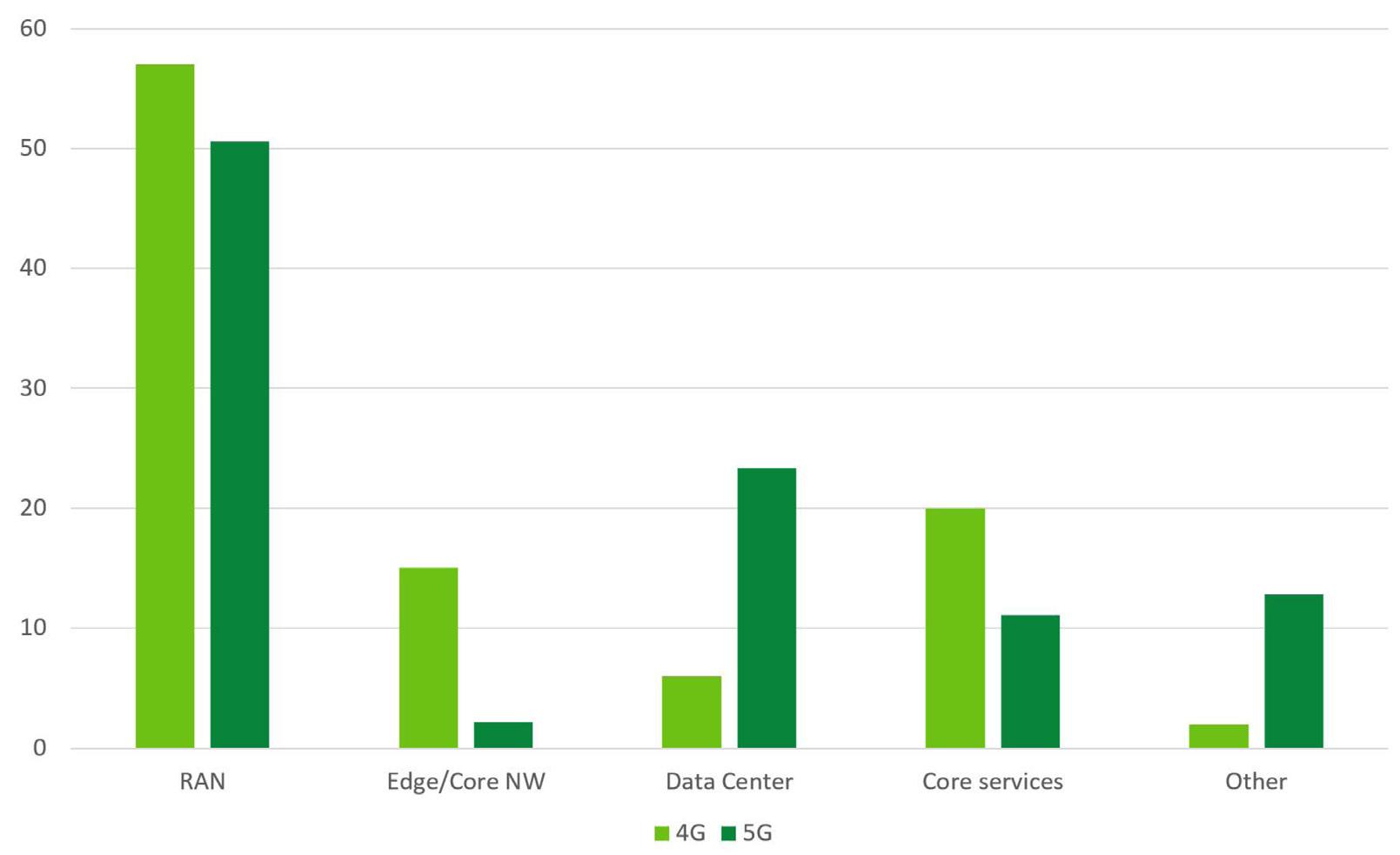
Sustainability is at the heart of 6G research, not just in telecom networks and equipment, but throughout the supply chain.
KeysightFigure 1. According to Next G Alliance, the largest portion of energy use in wireless networks comes from the radio access network. Image courtesy of NextG Alliance
Statistics like these make power reduction an easy area to focus on for future networks. Service providers are already making efforts to shift towards renewable energy sources to power their networks, with approximately 46% of electricity coming from renewable sources globally. This is a good first step, but reducing the energy needed is still required. Work has begun in 5G to make base stations more efficient, and 6G looks to take those efforts to the extreme. Techniques such as turning off power amplifiers and other components when they are not actively used, sometimes referred to as “sleep mode” or “deep sleep mode,” have proven successful in early trials; further work is needed to refine and optimize. The systems must remain off for a certain period to save enough energy to offset the energy required to turn them off and back on again, as demonstrated in Table 1. Machine learning can help to solve this optimization problem and obtain better results than a rulebased approach.
Improving the energy efficiency of Open RAN architectures is paramount as the industry shifts to these highly virtualized, open topologies. The RAN Intelligent Controller (RIC) that is a part of the architecture defined by O-RAN alliance is well positioned to take advantage of machine learning and artificial intelligence. The xApps and rApps that run on the RIC can optimize a range of applications
level performance of Open RAN architectures and defining best practices around reducing power consumption and overall optimization are active areas of research. Development should continue to improve over time.
including power efficiency. Whether Open RAN architectures will achieve greater efficiency than traditional networks remains to be seen.
Manufacturers and operators of traditional single-vendor networks can look at the efficiency of an entire base station and make tweaks throughout the entire chain to get the desired performance. That’s impossible with multivendor Open RAN systems — each component may be optimized for its individual function but could have worse overall performance when cascaded together with network components from other vendors. Looking at the system-
The power required to run a network is just one aspect of sustainability. With the shift towards more virtualization in the RAN, servers in data centers that run these virtual network functions will continue to use a larger portion of the network’s power needs. Most data centers today are, however, already highly optimized for power efficiency. Most of the cost to run them comes from electricity and the industry has spent years to reduce electricity costs by using evaporative cooling to keep data centers cool [4]. Evaporative cooling has become the de-facto cooling method because it uses significantly less electricity than other cooling methods. The tradeoff, however, is that it uses massive amounts of water. Estimates from the Water Resources Center at Texas Tech University show that a typical data center uses about the same
amount of water as a city of 30,000 to 50,000 people, and this high-water cost is causing cities in drought-prone climates to push back about building data centers. In 2020, Microsoft pledged to find a way to recycle water and be “water positive” by 2030 [6]. This is a step in the right direction; efforts like this need to continue and become adopted industry wide to make our shift to virtualized wireless networks green.
As an industry, and as consumers of mobile devices, we must look at the entire supply chain and lifecycle of our devices. Improving resource efficiency and recycling of electronics and batteries, using more sustainable materials, and using new materials for batteries are all important research areas for 6G sustainability. To define goals around sustainability and efficiency, new metrics and keyperformance indicators (KPIs) need to be developed and standardized. One challenge that the telecom industry must solve to create new metrics and KPIs is measuring the total carbon footprint of a wireless network.
Emissions are grouped into three different types: scope 1, 2, and 3 (Figure 2). Scope 1 emissions are direct emissions. These emissions include those from burning coal to create electricity at a power plant or emissions from vehicles in a company fleet. Scope 1 emissions are typically the easiest to measure.
Scope 2 emissions are emissions created from indirect use and come from purchased things such as electricity, heating, or cooling. For example, Scope 2 emissions can be reduced by purchasing electricity generated by renewable sources. They can also be measured with relative ease, but it requires transparency from vendors and suppliers.
Scope 3 emissions, classified as indirect emissions related to the upstream and downstream supply chain, account for the largest portion of emissions for most companies. They are the most difficult to measure and the most difficult to reduce. The telecom industry needs close partnership and collaboration between all vendors and suppliers across the entire supply chain. Efforts are underway to better measure emissions and to create standards around sustainability. These efforts will give both industry and consumers the transparency and clarity needed to make 6G green.
Enabling sustainability in other industries
5G brought a massive increase in the number of devices connected to cellular networks. That number will continue to grow as use cases such as private networks and the industrial internet of things reach critical mass. Massive amounts of data created by smart devices in combination with AI and ML built into 6G will give the industry deep insights that could appear in a wide variety of sustainability related applications.
In the manufacturing sector, having wireless connected machines will help with predictive maintenance by analyzing trend data and monitoring machine performance. Such activities can improve yield through trend and failure analysis. Augmented and virtual reality will make it easier for humans to interact with machines, helping them to troubleshoot problems quickly and reduce downtime. In farming, IoT devices connected to 5G and 6G can monitor soil conditions and help optimize the use of water and fertilizer. In automotive, V2X has started to define a way for cars to communicate with each other and the cellular infrastructure. 6G looks to leverage joint communications and sensing to help cars “see.” These added improvements will help autonomous vehicles become more advanced, which has the potential to greatly reduce traffic and some of the waste and inefficiencies associated with driving. As more devices and machines become wirelessly connected, we have an opportunity to optimize how they operate and reduce their carbon footprint.
Many challenges lie ahead for building a
sustainable, green wireless communications ecosystem. Developing and standardizing on ways to measure and communicate sustainability are crucial. Consumers will benefit from and are asking for markings such as the U.S Energy Star rating. Consumer demand for sustainable wireless technology is driving change around the world. Having a transparent, consistent, and easy-to-read rating system will let consumers make informed purchasing decisions. Standardizing on sustainability measurements will let companies quantify and improve the performance of their devices and systems. The focus and attention on sustainability in wireless communications shows the industry is serious about tackling these challenges - 6G can make the world a better place.
[1] “Country Analysis Executive Summary: China,” U.S Energy Information Administration, August 8, 2022. https://www.eia.gov/international/analysis/country/CHN
[2] “China 5G and Data Center Carbon Emissions Outlook 2035,” Greenpeace. https://www.greenpeace. org/static/planet4-eastasia-stateless/2021/05/ a5886d59-china-5g-and-data-center-carbon-emissionsoutlook-2035-english.pdf
[3] “Going green: benchmarking the energy efficiency of mobile,” GSMA Intelligence, June 2021. https:// data.gsmaintelligence.com/api-web/v2/research-filedownload?id=60621137&file=300621-Going-Greenefficiency-mobile.pdf
[4] Roland Kinch, “Understanding the benefits of evaporative cooling,” Data Center Dynamics, Dec. 2, 2016. https://www.datacenterdynamics.com/en/opinions/ understanding-the-benefits-of-evaporative-cooling/
[5] Olivia Solon, “Drought-stricken communities push back against data centers,” NBC News, June 19, 2021. https://www.nbcnews.com/tech/internet/ drought-stricken-communities-push-back-against-datacenters-n1271344
[6] Brad Smith, “Microsoft will replenish more water than it consumes by 2030.” https://blogs.microsoft. com/blog/2020/09/21/microsoft-will-replenish-morewater-than-it-consumes-by-2030/
RAN intelligent controllers, as defined by O-RAN Alliance, let cellular operators deploy intelligent RAN optimization applications. E2 is a key interface defined by O-RAN Alliance, but there are challenges in practically using it.
By Sridhar Bhaskaran, Rakuten SymphonyOpen radio-access networks (Open RAN) disaggregate a cell tower’s baseband unit into three units. The 5G Open RAN architecture specified by 3GPP separates functions into a centralized unit (CU) and distributed unit (DU), where these functions were otherwise contained in the baseband unit, which also included the radio. These units provide network operators with the ability to install units from different vendors rather than rely on a single source, enabling customized RANs. This disaggregation, however, depends on interoperable RAN units connected through standardized hardware and software interfaces. That’s more easily said than done. One of these interfaces is the E2 interface. Here’s where the E2 interface fits into a RAN and how it works.
The O-RAN Alliance has defined a disaggregated architecture of the 4G and 5G RAN. Some of the key aspects of disaggregated architecture are:
• Lower layer split: splitting the physical layer with the lower part of the physical layer running in a radio unit (RU) and the upper part of the physical layer running in the O-DU.
• Non-real-time RIC: running slower timescale control loop logic greater than 1 second.
• Near real-time RIC: running the low latency timescale control loop logic operating between 10 ms and 1 sec timescale.
• Service management and orchestration (SMO): running the management and orchestration of the RAN network functions. The non-RT RIC can be colocated with the SMO.
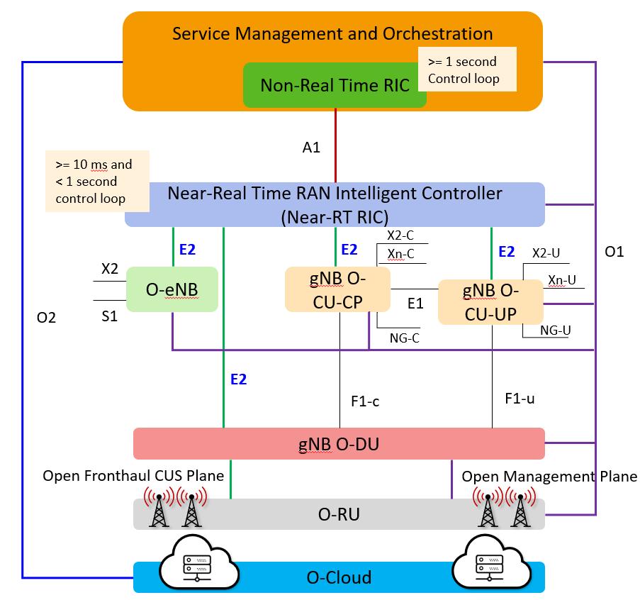
3GPP further specified a control-user plane split in the CU, splitting it into the CU-control plane (CU-CP) and the CU-user plane (CU-UP). The Open RAN concept further disaggregates the DU into two parts: the radio unit (O-RU), which runs the lower physical layer functions and the O-DU, which runs the higher physicallayer functions and the rest of the 3GPPdefined DU functions. When the 3GPP defined CU-CP and CU-UP functions, it also calls for additional interfaces defined by the O-RAN Alliance called O-CU-CP and O-CU-UP. (The term “interface” refers to the network protocol
interface carrying some payload information for software-based control of the Open RAN functions. When a 5G radio base station — called gNodeB or gNB — follows the O-RAN Alliance split architecture, they are called gNB O-DU, gNB O-CU-CP, and gNB O-CU-UP.)
The O-RAN Alliance has also specified splitting intelligence away from the CU-CP, CU-UP, and the DU into the RIC. You can view the RIC as a RAN’s software-defined network (SDN) controller. O-RAN Alliance has defined inner and outer levels of closed-loop control of the RAN through the RIC. The outer loop
is responsible for longer timescale (greater than 1 sec) control functions handled by non-real time RIC. In the inner loop, the near-real time RIC controls shorter timescale functions in the 10 msec to 1 second time scale.
For the inner loop, low latency control of the Open RAN network functions O-DU, CU-CP, or CU-UP, the O-RAN Alliance has defined the E2 interface; a network interface carrying events, control, and policy information to the Open RAN network functions.
Figure 1 shows the logical architecture. The O-RU is a physical appliance while the other components — gNB O-DU/ gNB O-CU-CP/gNB O-CU-UP/OeNB — can be either physical appliances or virtualized instances running over an O-Cloud layer. The interface lines shown in green are low-latency interfaces. The interface lines shown in purple are management plane interfaces, and the interfaces shown in black are the 3GPP-defined interfaces.
Traffic steering
QoS-based resource optimization
Massive MIMO optimization
• Load balancing handovers
• Selection of CA Scell/ENDC SN.
• Service based traffic steering.
• Monitor QCI/5QI specific statistics.
• Update resource allocation policies in RAN network functions.
• Monitor PRB utilization, UE level statistics from DU.
• Aid DU in massive MIMO beamforming and MU-MIMO pairing of users so that multiple UEs are scheduled in the same time-frequency resources but in different beams.
RAN slice SLA assurance
RAN analytics information exposure
General reporting of PM counters for all the above
• Monitor slice specific KPIs.
• Update resource partition per slice to meet SLA.
• Stream near-real time RAN statistics for analytics on QoE.
• All measurements are identified based on 3GPP defined measurement names (TS 28.552 and TS 32.425).
• Reporting granularity from 1 ms.
Role
The near-RT RIC is a platform that allows closed-loop control of RANoptimization applications to be onboarded as xApps. The xApps use platform services available in
the near-RT RIC to communicate with the downstream network functions through the E2 interface, where the downstream network functions can be gNB O-DU, gNB O-CU-CP, gNB O-CU-UP, or O-eNB. The E2 interface supports the following functions:
• Allows southbound nodes to set up the E2 interface and register the list of applications the southbound nodes support.
• Allows xApps running in the near-RT RIC to subscribe for events from the southbound nodes such as prescribe an action to execute upon encountering an event where the action can be to report the event, report, and wait for further control instructions from the xApp, or execute a policy.
• Provide control instructions.
Through these broad functionalities, the E2 interface is currently specified to support the RAN optimization use cases in Table 1.
The use cases in Table 1 occur through RAN control mechanisms including radio bearer control, radio resource allocation, connected mode mobility control, radio access control, carrier aggregation and dual connectivity control, and idle mode mobility control.
Now that we know the organization of RAN functions, we look at the E2 interface. Figure 2 shows the E2 interface protocol stack.
An application protocol called E2AP is specified by O-RAN Alliance over SCTP/IP as the transport protocol. On top of E2AP, application-specific controls and events are conveyed through E2 service models (E2SM). The xApps in the Near-RT RIC use the E2SMs.
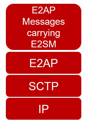
To get a deeper understanding of the E2 interface, you should first understand the E2AP terminologies. Key E2AP terminologies include:
• E2 node: in the O-RAN architecture, each of the disaggregated network function O-CU-CP, O-CU-UP and O-DU of a gNB or a combined O-eNB are called the E2 nodes. E2 nodes support E2 interface towards near RT-RIC and O1 interface towards non-RT RIC.
• RAN function: a specific function in an E2 Node; examples include network interfaces (i.e. X2AP, F1, S1AP, Xn, NGc) and RAN internal functions handling user equipment context handlers, call handlers, paging, and so on.
• RIC service: a service provided on an E2 Node to provide access to messages and measurements and / or enable control of the E2 Node from the Near-RT RIC. RIC Services Include:
• RAN function ID: local identifier of a specific RAN function within an E2 Node that supports one or more RIC Services using a specific E2 Service Model. Note that same E2SM may be used by more than one RAN function in the same E2 Node.
• Style: for each RIC service, different types of data can be grouped as a style. A given E2SM may support many styles for each RIC service.
An E2 node can consist of one or many RAN functions. Each RAN function is identified by a RAN function ID. The E2 node advertises to the E2SM the RAN functions it supports using the RAN Function OID as the identifier. Figure 3 shows a logical view of an E2 node. Each RAN function exposes a RAN function definition through its E2SM, which could contain some or all of the following definitions.
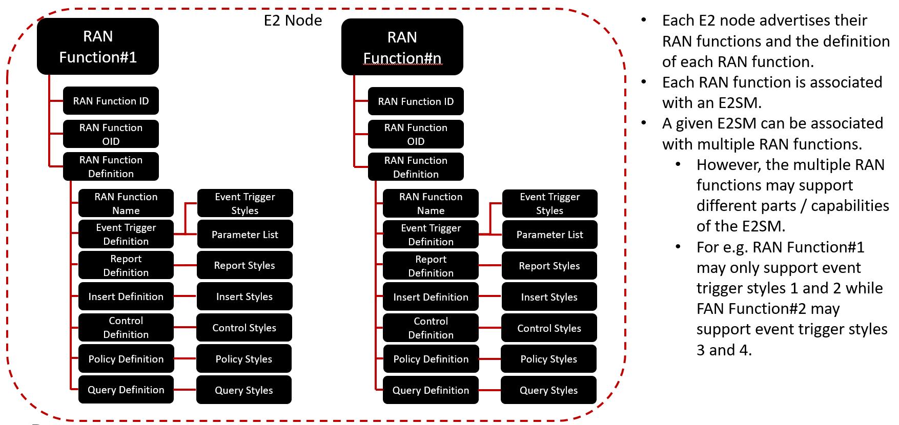
• Event trigger definition: contains the definition of event triggers for which E2 node can be requested to report the event to near-RT RIC. The definition includes the event styles supported by the E2 node.
• Report definition: contains the definition of event reports and the report styles supported by the E2 node.
• Insert definition: contains the definition of information on which the E2 node has to exhibit “report and wait for control” semantics and the insert styles supported by the E2 node.
• Control definition: contains the definition of attributes/ configurations/call parameters to be controlled on the E2 node and the control styles supported by the E2 node.
• Policy definition: contains the definition of policy to apply at the E2 node when the specified event trigger is hit.
The messages and procedures of the E2AP protocol are structured as given below:
• Global procedures are responsible for the setup and maintenance of the E2 link between the near-RT RIC and the E2 nodes. The global procedures supported on the E2 interface include E2 interface setup, E2 node configuration update, E2 service update, E2 connection update, E2 reset, and E2 error indication.
• Functional procedures are responsible for getting information and events from the E2 nodes to provide further control or policy information back to the E2 nodes. The functional procedures include RIC subscription request/deletion request, RIC indication (for REPORT service and for INSERT service from E2 node to nearRT RIC) and RIC control request (for controlling parameters in E2 node — from near-RT RIC to E2 node).
Using the procedures defined above, a general workflow to be followed between the near-RT RIC and E2 node appears in Figure 4.
First, the interface link between the E2 node and the Near-RT RIC is set up. During this process, the E2 node advertises the list of RAN functions it supports and the corresponding E2SM supported for each RAN function. The xApps running in the Near-RT RIC subscribe to the E2 node, providing the event triggers and what actions to perform upon hitting those event triggers. If the action to perform is either REPORT or INSERT, the E2 node notifies the near-RT RIC when the event occurs. If the notification is due to an INSERT action, the xApp in the near-RT RIC provides a corresponding CONTROL request to the E2 node. If the notification is due to a REPORT action, the xApp in the near-RT RIC may
provide a subsequent CONTROL request to the E2 node. Through the CONTROL request, the xApp can control the call processing, radio resource allocation, handover control, idle mode mobility control, radio admission,

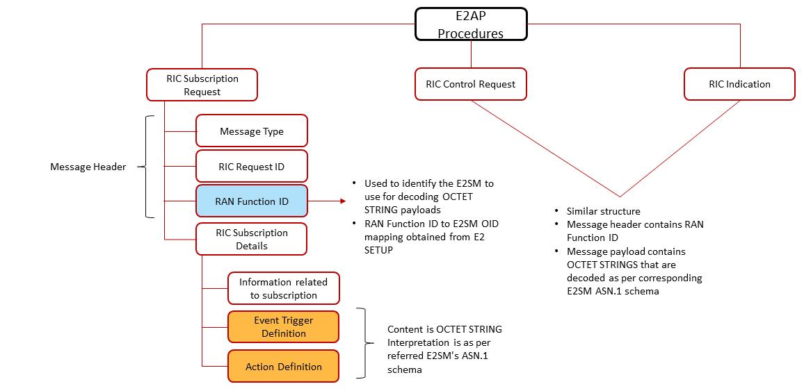
carrier aggregation, and dual connectivity behaviors on a per-user (UE) basis in the E2 node. All the red-colored items in Figure 3 are carried as opaque payloads over E2AP as OCTET STRINGs. The interpretation of these
OCTET STRINGS into the right structures is done based on the “RAN Function ID” carried in the message headers and the E2SM the corresponding RAN function advertised during the E2 setup process.
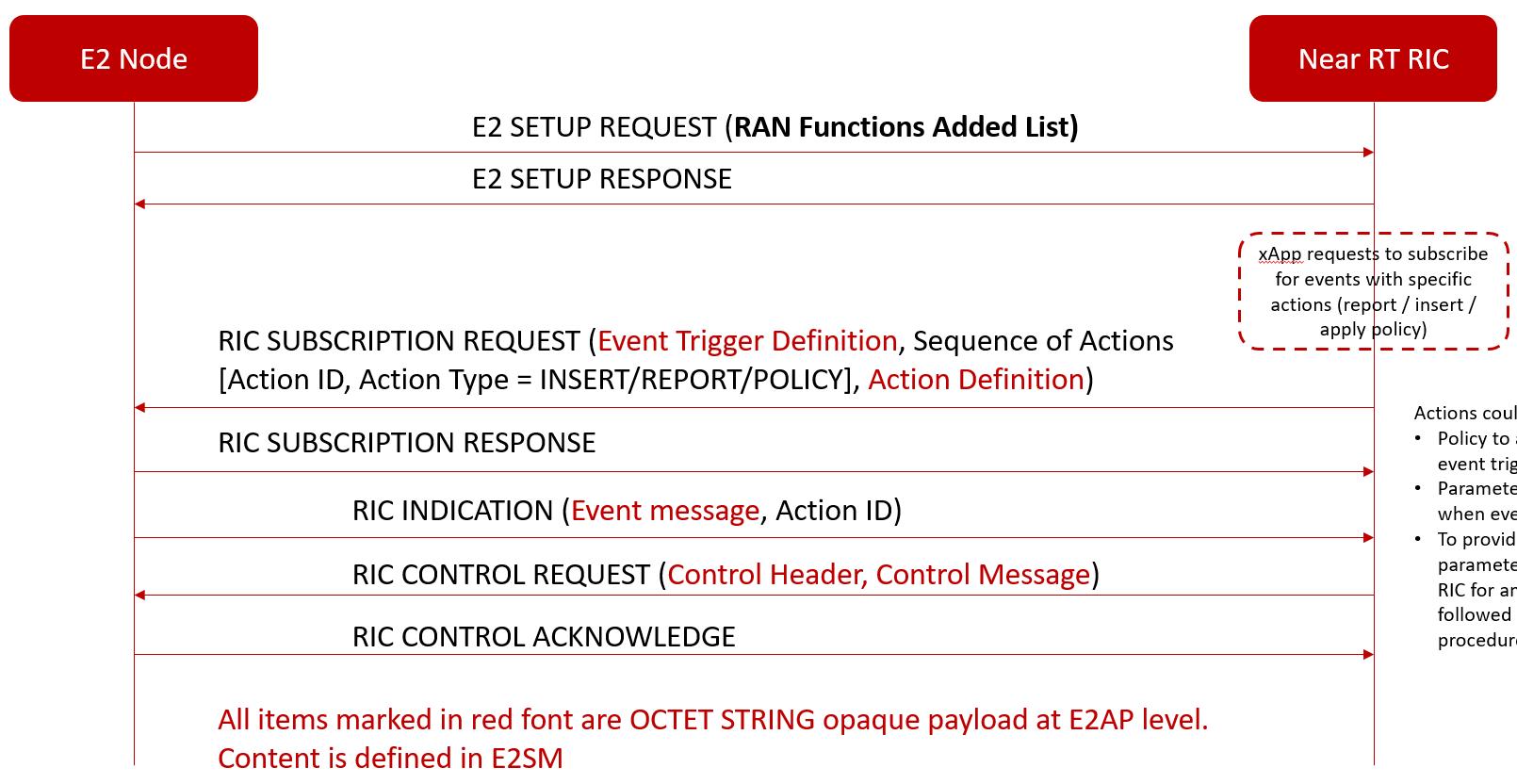
The E2AP protocol is defined generically to allow any application to run on top of it. Applications use E2 service models (E2SM) for the control and handling of specific RAN functions in E2 nodes. The messages and information carried in both E2AP and E2SM are defined using ASN.1 PER schema. The RAN function-related event triggers, actions and controls are carried as an OCTET STRING payload over the E2AP messages. The OCTET STRING is decoded using the ASN.1 PER schema of the E2SM. The RAN function E2SM ASN.1 to use for such decoding is identified by the “RAN function ID” in the header of the E2AP messages. The mapping of the “RAN function ID” to the E2SM OID is obtained from the E2 setup procedure. In the standard defined E2SMs, most of the information is again contained as OCTET STRING. The interpretation of such OCTET STRING is based on the normative tables in the respective E2SM specifications. Generally, such OCTET STRINGs refer to 3GPP-defined information. Such 3GPP-defined information is again to be decoded using 3GPP ASN.1 PER schema. This structuring of an E2AP message is shown in Figure 5.
While such a design of E2AP procedures allows for independent evolution of 3GPP and O-RAN specifications and makes the maintenance of O-RAN E2-related specifications easier, it has the following issues from a practitioner’s point. These make it challenging to adopt the E2SM models “as is” from standards:
• When message traces are taken, it is extremely hard to decode them with message parsers such as Wireshark because the decoding logic relies on prior information where “RAN function ID” was mapped to a specific OID in the E2 setup procedure. This makes the protocol decoding completely stateful. Network protocols are generally defined such that each message is self-contained and decodable in itself — each message is stateless on its own.
• Debugging the interface requires implementing stateful protocol dissectors, for example in Wireshark.
Conclusion
The original intent of the E2 interface was to allow any application (vendor-defined, operator defined, and third-party) to have a closed loop, low latency, feedback-based control of the RAN. The design of the E2 interface and the E2AP protocol makes integration and debugging hard.
To avoid such nested OCTET STRING decoding, alternate approaches taken include defining custom E2SMs with self-contained ASN.1 PER schema, which don’t define further nested OCTET STRINGs. Resorting to such custom approaches, however, defeats the purpose of standardization. If you were to develop applications using standarddefined E2SMs that are easy to integrate and debug, you need protocol dissectors that support full dissection and decoding of E2AP and E2SM in a stateful manner.

The demand for high data throughput, low power, and longer battery life is driving much of the breakthroughs and evolutions in connectivity technology.

In this Design Guide, we present the need-to-know basics, as well as the technology fine points aimed at helping you and your designs keep pace and stay competitive in the fast-changing world of connectivity.
BROUGHT TO YOU BY:





FOR UPCOMING AND ON-DEMAND WEBINARS, GO TO: www.designworldonline.com/designworld-online-events-and-webinars
DESIGN WORLD WEBINAR SERIES: Where manufacturers share their experiences and expertise to help design engineers better understand technology, product related issues and challenges.


PRICING & AVAILABILITY
Get real-time pricing and stock info from authorized distributors and manufacturers.
View and download product data sheets and technical speci cations.
Compare options from suppliers and buy direct from distributors and manufacturers.

DesignFast is a search engine for nding engineering components and products. With DesignFast, engineers and sourcing professionals can quickly search for products, compare prices, check stock, view data sheets and go direct to the supplier for purchase.

DesignFast aggregates product data from thousands of suppliers and distributors and makes it available for searching. DesignFast provides pricing, availability and product data sheets for free download.
designfast.com


