POWER ELECTRONICS HANDBOOK

A SUPPLEMENT TO DESIGN WORLD FEBRUARY 2023 How to control dc microgrids Page 12 Simplifying designs for high power density applications Page 16 Selecting dc-dc converters for railway applications Page 45


The most demanding applications require the world’s most reliable components. For over 50 years PICO Electronics has been providing innovative COTS and custom solutions for Military, Commercial, Aerospace and Industrial applications. Our innovative miniature and sub-miniature components are unsurpassed in any industry. PICO Electronics’ products are proudly manufactured in the USA and are AS9100D Certified.

To learn more about our products and how you can benefit from our expertise visit our website at picoelectronics.com or call us today at 800-431-1064.
TRANSFORMERS
• Ultra Miniature Designs
• MIL-PRF-27/MIL-PRF-21038
• QPL Approved DSCC

• Audio/Pulse/Power/EMI Multiplex Models Available

• For Critical Applications, Pico Continues to Be the Industry Standard
Surface Mount & Thru Hole Military • COTS • Industrial
• MIL/COTS/Industrial Models
• Regulated/Isolated/Adjustable Programmable Standard Models
• New High Input Voltages to 900VDC
• AS9100D Facility/US Manufactured
• Military Upgrades and Custom Modules Available

VISIT OUR EXCITING NEW WEBSITE: www.picoelectronics.com Transformers & Inductors, DC-DC Converters,AC-DC Power Supplies The big name in miniature components. The big name in miniature components.
CONVERTERS
1-300
DC-DC
2V to 10,000 VDC Outputs —
Watt Modules
& INDUCTORS
Think Pico SmallOver 5000 Std Ultra Miniature
.18" think... ht.
Certified to AS9100D ISO 9001:2015 low
Call Toll Free: 800-431-1064 E Mail: Info@picoelectronics.com • FAX: 914-738-8225 143 Sparks Ave, Pelham, NY 10803 PICO Electronics Inc.
profile from
08 Extended Power Range GaN-based USB-C adapters and chargers deliver increased performance

An innovative, highly integrated combo controller for the joint control of the PFC and the hybrid flyback stage.
12
How to control dc microgrids

Microgrids are a great way to power locations where grid connections are unreliable, though it can be tricky to control them in robust ways.
16 Simplifying designs for high power density applications

High-density power module technology for FPGAs, SoCs, & ASICs makes designing easy by providing the highest power densities in the smallest spaces.
20 Power optimization techniques for low-power signal chain applications
Several system-level techniques are available that can make signal chains designs more power efficient and reduce system design complexity.

26 A better way to handle dc-dc converter hold-up times


Converters with built-in holdup circuitry reduce the size and requirements for input capacitors.
28 Circuit boards don’t behave the way you think they do Circuit designers increasingly must concentrate on the design of transmission lines, or the “spaces” between traces, instead of the
32 The case for AEC-Q semiconductors in non-automotive uses


Specifying parts built in AEC-Q-certified fabs is an inexpensive way of creating exceptionally reliable, long-lasting designs.
34 Enabling a do-it-yourself hot-swap circuit design using a hybrid architecture
Implementing a hybrid hot-swap circuit can make your life easier by eliminating a complex design process while ensuring robust protection, reduced solution size, and cost.
38 Bidirectional power supplies support new UPS requirements

Bidirectional power supplies dynamically direct power from multiple sources to different loads, some of which are also power sources at other times.
42 Key considerations when integrating high voltage dc-dc converters into critical applications
Knowing precise parameters up front goes a long way to ensuring your critical application meets performance expectations.

45 Selecting dc-dc converters for railway applications
The wide range of voltages and power levels required in modern trains puts a special focus on the role of the dc-dc converter.
CONTENTS POWER ELECTRONICS HANDBOOK • FEBRUARY 2023 CHECK US OUT on ISSUU.COM! CONNECT WITH US!
Circuit Protection

•Fuses & Fuse Accessories
•PTC Resettable Fuses
•TVS Diodes
•Varistors
•ESD Suppressors
Supercapacitors Magnetics

•Coin Cells
•Cylindrical Cells
•Large Cells
•Modules
•Systems
•Hybrid Cells
•Power Inductor
•High Current
•Transformers
•EMC (RF / EMI) Filters
•DC-DC Converters
Terminal Blocks Sensors
•Single Row / Barrier Strip
•Euromag / IEC Style
•Edge Connector
•Temperature Sense
•Current Sense
Eaton offers a range of electronics components that include power and EMC magnetics solutions, circuit protection, supercapacitors and terminal blocks products. These products serve customers in computing, consumer, energy, industrial, medical and transportation markets. Learn more on our website: Eaton.com/electronics Contact us: Eaton.com/ELXContactUs


DESIGN WORLD
FOLLOW THE WHOLE TEAM ON TWITTER @DESIGNWORLD
EDITORIAL
VP, Editorial Director Paul J. Heney pheney@wtwhmedia.com

@wtwh_paulheney
Senior Contributing Editor Leslie Langnau llangnau@wtwhmedia.com
@dw_3Dprinting
Senior Editor
Aimee Kalnoskas akalnoskas@wtwhmedia.com @eeworld_aimee Editor Martin Rowe mrowe@wtwhmedia.com @measurementblue
Associate Editor Emma Lutjen elutjen@wtwhmedia.com
Executive Editor Lisa Eitel leitel@wtwhmedia.com @dw_LisaEitel
Senior Editor Miles Budimir mbudimir@wtwhmedia.com
@dw_Motion
Senior Editor Mary Gannon mgannon@wtwhmedia.com
@dw_MaryGannon

Managing Editor Mike Santora msantora@wtwhmedia.com
@dw_MikeSantora
VP, Creative Services Mark Rook mrook@wtwhmedia.com
@wtwh_graphics
Senior Art Director Matthew Claney mclaney@wtwhmedia.com @wtwh_designer
Senior Graphic Designer Allison Washko awashko@wtwhmedia.com @wtwh_allison
Graphic Designer Mariel Evans mevans@wtwhmedia.com @wtwh_mariel
Director, Audience Development Bruce Sprague bsprague@wtwhmedia.com
IN-PERSON EVENTS
Events Manager Jen Osborne jkolasky@wtwhmedia.com @wtwh_Jen
Events Manager Brittany Belko bbelko@wtwhmedia.com
Event Marketing Specialist Olivia Zemanek ozemanek@wtwhmedia.com
Event Coordinator Alexis Ferenczy aferenczy@wtwhmedia.com
MARKETING
VP, Digital Marketing Virginia Goulding vgoulding@wtwhmedia.com @wtwh_virginia
Digital Marketing Coordinator

Francesca Barrett fbarrett@wtwhmedia.com @Francesca_WTWH
Digital Design Manager Samantha King sking@wtwhmedia.com
Marketing Graphic Designer Hannah Bragg hbragg@wtwhmedia.com
Webinar Manager Matt Boblett mboblett@wtwhmedia.com
Webinar Coordinator Halle Kirsh hkirsh@wtwhmedia.com
Webinar Coordinator Kim Dorsey kdorsey@wtwhmedia.com
FINANCE
CREATIVE SERVICES & PRINT PRODUCTION Controller Brian Korsberg bkorsberg@wtwhmedia.com
Accounts Receivable Specialist Jamila Milton jmilton@wtwhmedia.com
ONLINE DEVELOPMENT & PRODUCTION
Web Development Manager B. David Miyares dmiyares@wtwhmedia.com @wtwh_WebDave
Senior Digital Media Manager Patrick Curran pcurran@wtwhmedia.com @wtwhseopatrick
Front End Developer Melissa Annand mannand@wtwhmedia.com
Software Engineer David Bozentka dbozentka@wtwhmedia.com
Digital Production Manager Reggie Hall rhall@wtwhmedia.com
Digital Production Specialist Nicole Lender nlender@wtwhmedia.com

Digital Production Specialist Elise Ondak eondak@wtwhmedia.com
Digital Production Specialist Nicole Johnson njohnson@wtwhmedia.com
VP, Strategic Initiatives Jay Hopper jhopper@wtwhmedia.com
VIDEOGRAPHY SERVICES
Videographer Garrett McCafferty gmccafferty@wtwhmedia.com
Videographer Kara Singleton ksingleton@wtwhmedia.com
PRODUCTION SERVICES
Customer Service Manager Stephanie Hulett shulett@wtwhmedia.com
Customer Service Representative Tracy Powers tpowers@wtwhmedia.com
Customer Service Representative JoAnn Martin jmartin@wtwhmedia.com
Customer Service Representative Renee Massey-Linston renee@wtwhmedia.com
Customer Service Representative Trinidy Longgood tlonggood@wtwhmedia.com
WTWH Media, LLC
1111 Superior Ave., Suite 2600
Cleveland, OH 44114
Ph: 888.543.2447

FAX: 888.543.2447
DESIGN WORLD does not pass judgment on subjects of controversy nor enter into dispute with or between any individuals or organizations. DESIGN WORLD is also an independent forum for the expression of opinions relevant to industry issues. Letters to the editor and by-lined articles express the views of the author and not necessarily of the publisher or the publication. Every effort is made to provide accurate information; however, publisher assumes no responsibility for accuracy of submitted advertising and editorial information. Non-commissioned articles and news releases cannot be acknowledged. Unsolicited materials cannot be returned nor will this organization assume responsibility for their care.
DESIGN WORLD does not endorse any products, programs or services of advertisers or editorial contributors. Copyright© 2023 by WTWH Media, LLC. No part of this publication may be reproduced in any form or by any means, electronic or mechanical, or by recording, or by any information storage or retrieval system, without written permission from the publisher.
SUBSCRIPTION RATES: Free and controlled circulation to qualified subscribers. Non-qualified persons may subscribe at the following rates: U.S. and possessions: 1 year: $125; 2 years: $200; 3 years: $275; Canadian and foreign, 1 year: $195; only US funds are accepted. Single copies $15 each. Subscriptions are prepaid, and check or money orders only.
SUBSCRIBER SERVICES: To order a subscription or change your address, please email: designworld@omeda.com, or visit our web site at www.designworldonline.com
POSTMASTER: Send address changes to: Design World, 1111 Superior Ave., Suite 2600, Cleveland, OH 44114


6 DESIGN WORLD — EE NETWORK 2 • 2023 eeworldonline.com | designworldonline.com
2011 - 2020 2014 Winner 2014 - 2016
2013- 2017
Ferrite Cores with Distributed Air Gaps


Increased power density and optimized efficiency
TDK’s new standards for ferrite cores with distributed air gaps, enables increased power density and a further degree of downsizing compared to other technologies. In addition, cores with distributed air gaps offer the possibility to optimize the design of transformers and chokes in terms of efficiency and thermal performance.
• ETD, PQ and E cores with distributed air gaps are available as standard catalog types for many core sizes and various Al values.
• Ferrite cores with distributed air gaps allow for the use of a larger winding areas by reducing the fringing flux losses, offer significantly increased power density and improve the winding window fill ratio.

Typical Applications include:
– Onboard chargers and DC-DC converters for xEV vehicles


– Charging stations for EV
– Solar inverters


– Uninterruptible power supplies (UPS)
– Industrial switch-mode power supplies
www.tdk.com
Extended Power Range GaN-based USB-C adapters and chargers deliver increased performance
Bredemeier, Principal Engineer for Power Systems and Solutions Division, Infineon Technologies
TheUniversal Serial Bus Power Delivery Specification (Revision 3.1, Version 1.1)

(USB-PD) standard enables higher power levels of up to 240 W. The wide output voltage range of 5 V to 48 V, however, raises new challenges for currently used converter topologies. The combination of an AC-DC power factor correction (PFC) boost and a DC-DC hybrid flyback (HFB) stage, also known as an asymmetrical half-bridge flyback topology, can provide the right solution for USB-PD chargers and adapters with wide input and output voltage ranges. Before discussing this approach, a little background on the latest USB standard is in order.
USB-PD Extended Power Range standard
The latest IEC 62680-1-2:2022 specification defines a power delivery system that addresses all elements of a USB system. This includes hosts, devices, hubs, chargers, and cable assemblies. The USB-PD Extended Power Range (EPR) standard with 28 V, 36 V, and 48 V fixed voltages offers a universal AC-DC adapter for many different purposes, charging a whole range of end devices, from smartphones to gaming laptops, up to power tools, and even e-bikes. It defines an adjustable voltage supply (AVS) mode that allows the device being powered to request intermediate voltages between 15 V and up to the maximum available fixed voltage in these systems. Electromagnetic compatibility, power factor correction, standby power, and average efficiency requirements raise challenges for the converter topologies
8 DESIGN WORLD — EE NETWORK 2 • 2023 eeworldonline.com | designworldonline.com POWER ELECTRONICS HANDBOOK
Topology Size Efficiency Comments PFC+Flyback Requires bulky transformer Good Limited in switching frequency. PFC+LLC+Buck Small Very good Output voltage range limitations require a buck converter that negates the inherent size and efficiency. PFC+Hybrid Flyback Very small Very good Wide output voltage range. Transformer size can be reduced considerably from conventional flyback variants.
Peter
delivery.
Table 1. Comparison of key design characteristics for mid-power/ wide output voltage power
An innovative, highly integrated combo controller for the joint control of the PFC and the hybrid flyback stage.
used up to now. Additionally, the size and, consequently, the power density becomes a more critical factor for the end users.
Design options for state-of-the-art mid-power range with wide output voltage range circuit topologies include PFC+Flyback, PFC+LLC+Buck, and PFC+Hybrid flyback topologies. Table 1 summarizes the characteristics of these approaches.
With its small size and efficiency, the PFC+Hybrid flyback topology was chosen to meet the latest USB-PD EPR V3.1 standard. This architecture also enables a high-power density with high power efficiency design to meet other international regulatory standards, such as the European Union Code of Conduct (EU CoC) Version 5 Tier 2 requirements for external power supplies, and the U.S. Department of Energy (DoE) Level VI.
Since a wide variety of devices now rely on USB Type-C for connection, communication, and power, the USB Implementers Forum (USB-IF) uses independent test labs to certify conformance to the standard before manufacturers can identify and claim conformance on specific products.
Other certifications, such as IEC623681:2018, “Audio/video, information, and communication technology equipment – Part 1: Safety requirements,” need to be considered as well. In this case, non-compliant products cannot be sold in major markets after the effective date.
XDP™ Digital Power Controllers
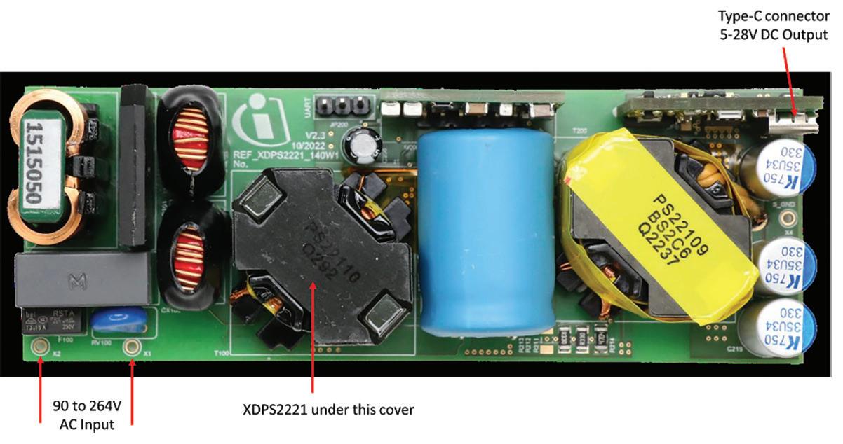
Allowing system designers to easily implement a USB-PD EPR solution, a highly integrated XDP™ controller XDPS2221 controls both the PFC and the hybrid flyback stages. This integration offers optimal control of both stages to deliver maximum performance. To further simplify the system designer’s task, a 140 W ACDC reference design has been developed that achieves a full load peak efficiency of up to 95 percent and a high-power density of 22.67 W/ in3 (uncased) while delivering an output voltage from 5 VDC to 28 VDC, with input voltage range from 90 VAC to 264 VAC.
Proposed architecture
To achieve the highest power density, the proposed two-stage solution consists of an AC-DC PFC boost stage and the DC-DC hybrid flyback, combined with synchronous
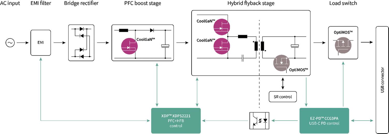
rectification (SR) at the output. Figure 1 shows the details of the converter architecture. Gallium nitride (GaN) power devices were chosen for the switches of the PFC+HFB power stage. In addition to the three CoolGaN™ IGLD60R190D1 600V enhancement mode (e-mode) devices, the architecture uses OptiMOS™ FETs for the load switch and SR control, and the EZ-PD™ controller CCG3PA CYPD3175 for communication with the end device and output voltage management.
The XDPS2221 integrates an AC-DC power factor correction controller with a DC-DC hybrid flyback (HFB) controller, also known as an asymmetrical half-bridge (AHB), into a single 9.9 x 3.9-mm DSO-14 package. The integration includes a high-side driver coupled with a coreless transformer and a low-side driver driving the high- and low-side switches of the HFB stage, as well as a driver for the PFC switch. It enables a simple system structure out of the traditional flyback topology and provides the performance of a resonant half-bridge converter. Regulatory requirements can easily be met through the coordinated operation of the two stages.
Integrating all gate drivers, the GaN 600 V high voltage start-up cell for the initial IC voltage supply, and the certified active X-capacitor discharge for IEC62368-1:2018 conformance allow for a low external bill of material (BOM) and component count. Based on the zero-voltage switching (ZVS) HFB topology and GaN-based power devices, the design brings efficiency across various line/ load conditions. With these features and inherent topology advantages, such as ZVS and resonant energy transfer for transformer size reduction, system designs using the XDPS2221 can achieve very high-power densities.
The combo IC controller features a synchronous PFC and HFB burst-mode operation. The converter is switched on and off during light or no load to reduce the standby power for the lowest possible no-load input standby power performance. The quasi-resonant multimode PFC stage is enhanced with automatic PFC enable/disable functionality and adaptive PFC bus voltage control to maximize average and light load efficiency. Optionally, the integrated PFC function can also be disabled to support the use case with any external PFC controller.
The hybrid flyback stage uses peak current control operation for well-controlled regulation and fast dynamic load response. To ensure ZVS operation under all conditions, the hybrid
9 DESIGN WORLD — EE NETWORK 2 • 2023 eeworldonline.com | designworldonline.com G a N-BASED USB-C
Figure 1. Proposed power architecture for a USB-PD EPR converter.
Figure 2. 140 W prototype USB-PD EPR 5 V – 28 V converter based on the XDPS2221 has a power density of 22.67 W/inch3
flyback features ZVS pulse insertion, including body diode cross-conduction prevention in the discontinuous conduction mode. Additionally, the XDPS2221 provides easy-to-configure parameters via a graphical user interface (GUI) to optimize system performance.
The embedded digital core of the integrated controller allows a sophisticated control algorithm to optimize the performance of both power stages. For optimum system efficiency and reduced standby power, the PFC stage will only be enabled depending on input and output voltage conditions and load conditions. In addition, a bus voltage target modulation, depending on the operation point of the HFB, helps to increase the efficiency even further.
To reach the highest power density, it is desired to maximize the efficiency at the maximum load, typically the worst case in terms of power losses. With the newly implemented PFC modulation, it is possible to improve the efficiency for the lower output voltage levels; the modulation can enhance efficiency by nearly five percent for the lowest output voltage.
The embedded digital core supports system fine-tuning by configurable parameters. This gives designers the flexibility to adapt to different power levels and application requirements. Additionally, very high-frequency switching applications can be supported and enable the usage of a planar transformer due to zero voltage switching and zero current switching (ZCS).
Practical prototype
To demonstrate the described advantages, a 140 W (28 V/5 A) prototype has been developed (Figure 2). In this case, two-layer PCBs and standard magnetic cores are utilized to achieve low system cost.
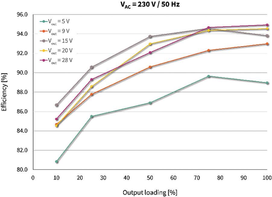
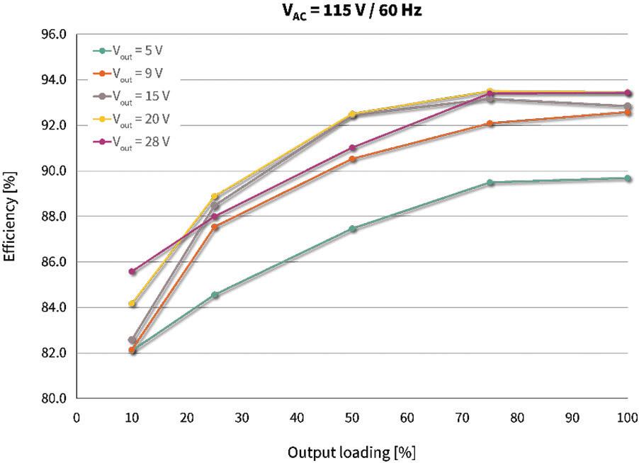
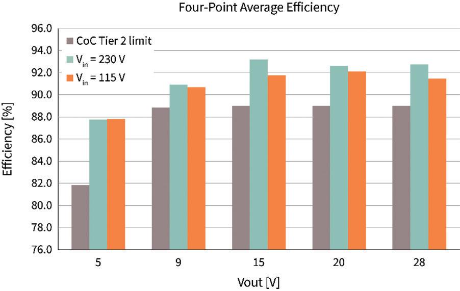
The efficiency results are shown in Figures 3 (low line) and 4 (high line). The results cover the output voltage range of 5 V – 28 V with load variation from 10 – 100%. The circuit reaches a peak efficiency of 95% at maximum load but stays above 80% efficiency at minimum load. This results in the following four-point average efficiency shown in Figure 5. With the integrated sophisticated control algorithm between PFC and HFB, the CoC Tier 2 limits can be easily achieved.
Due to the synchronous PFC and HFB burst mode operation, the standby losses in the input voltage that range from 90 VAC up to 264 VAC could be decreased below 70 mW over the entire input voltage range.
Meeting evolving standards
The USB-PD Extended Power Range standard defines requirements for power delivery in higher power ranges for a variety of applications that use the USB Type-C connector. Combining the HFB and the PFC-boost with the control strategy demonstrates the potential for USB-PD EPR adapters to reach high efficiencies from light load to maximum load. The highly integrated controller with combined PFC and HFB operation enables a simple design in a small size to achieve a high-power density. The benefits of the proposed solution have been demonstrated with a 140 W USB-PD EPR prototype achieving high peak efficiency of 95% and a power density of 22.67 W/in3 with a low-cost two-layer PCB.
10 DESIGN WORLD — EE NETWORK 2 • 2023 eeworldonline.com | designworldonline.com POWER ELECTRONICS HANDBOOK
Figure 3. Low line efficiency vs. output loading for a voltage range of 5 – 28 VDC.
Figure 4. High line efficiency vs. output loading for a voltage range of 5 – 28 VDC.
Figure 5. Four-point average efficiency results indicate that the CoC Tier 2 limits can be easily achieved.
Capacitor Solutions for Aerospace, Defense, Energy & Communications


Hybrid wet tantalum capacitors—the most power dense in the industry; SWaP optimized for missioncritical applications.


Patented ceramic capacitors for the most demanding high-frequency microwave, millimeter-wave, and 5G applications.


Multi-layer Polymer (MLP) capacitors, including our recently released hi-rel MLP capacitors, which provide the industry’s highest ripple current rating per C*V.
Standard and engineered high-reliability multilayer ceramic chip capacitors (MLCCs) and leaded MLC devices.


Visit us at APEC booth #842
How to control dc microgrids
Microgrids are a great way to power locations where grid connections are unreliable, though it can be tricky to control them in robust ways.
Daniel Zammit, Dept. Industrial Electrical Power Conversion, University of Malta
Microgrids
get a fair amount of press coverage these days thanks to their role in distributed power generation. A typical microgrid consists of distributed electrical power sources (e.g. photovoltaic systems, wind generation systems, etc.) and loads which together form a self sustainable electrical supply system, basically a small electrical grid.
The levels of control involved in a typical microgrid present challenges, giving rise to research opportunities aimed at perfecting the control systems that handle power converter integration in microgrid systems. Research in the field of dc microgrids spans topics ranging from control algorithms to improved load sharing among converters within the microgrid to algorithms that reduce operational costs,
all while simultaneoulsy trying to establish common standards with regard to control strategies, stabilization techniques, and standardization issues. Energy management within dc microgrids is also a popular research topic.
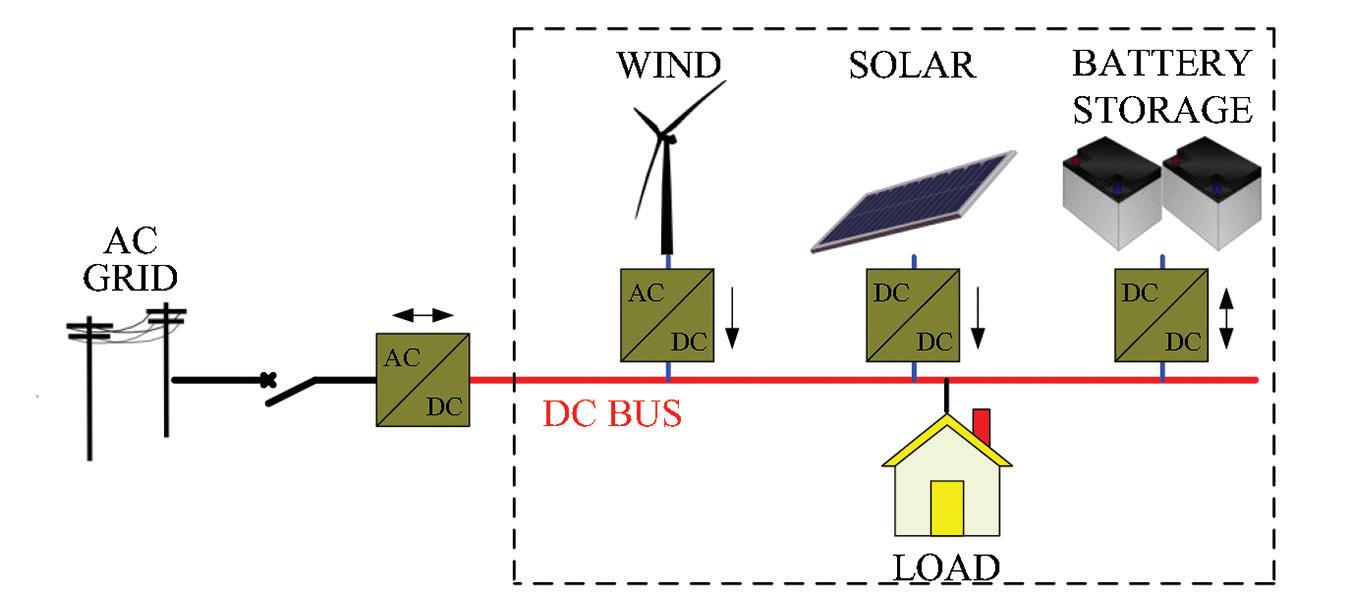
Microgrids can be ac, dc, or a combination of both. An attractive aspect of microgrids is the ability to connect with the grid as well as operate completely alone and autonomously in islanded mode. Of course, islanded mode operation is a great feature to have if the electrical grid fails. Different scenarios call for different ac or dc microgrid configurations. However, dc microgrids in particular are attracting a lot of research because they have lower conversion losses and fewer power conversion stages, no synchronization issues, and independence from power quality issues that arise on the ac grid.
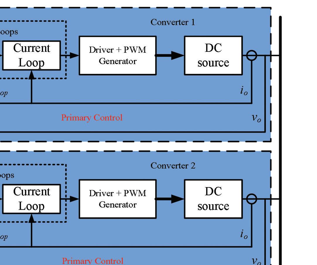
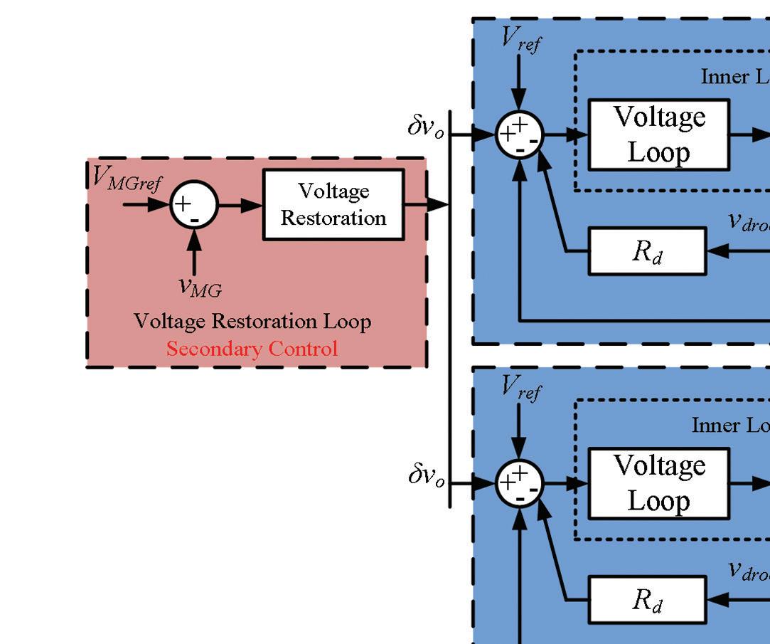
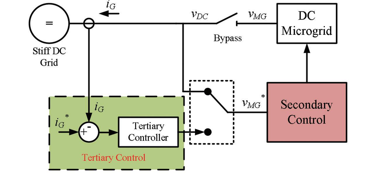
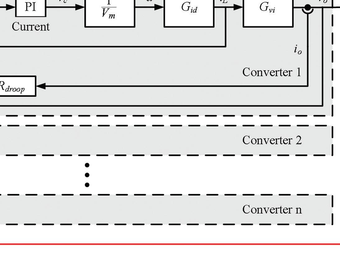
One of the main challenging aspects of microgrids is their internal controls. Different control systems within the microgrid system take care of the voltage, sharing of load current between the power converters, as well as charging and discharging of energy storage systems like batteries and supercapacitors. These control systems are generally organized in a hierarchical control system consisting of three levels: primary control local to each converter in the microgrid, including current and voltage control based on what’s called a droop control system; secondary control which restores deviations caused by the primary control, and tertiary control which handles the power flow between the microgrid and any outside electrical distribution system.
12 DESIGN WORLD — EE NETWORK 2 • 2023 eeworldonline.com | designworldonline.com
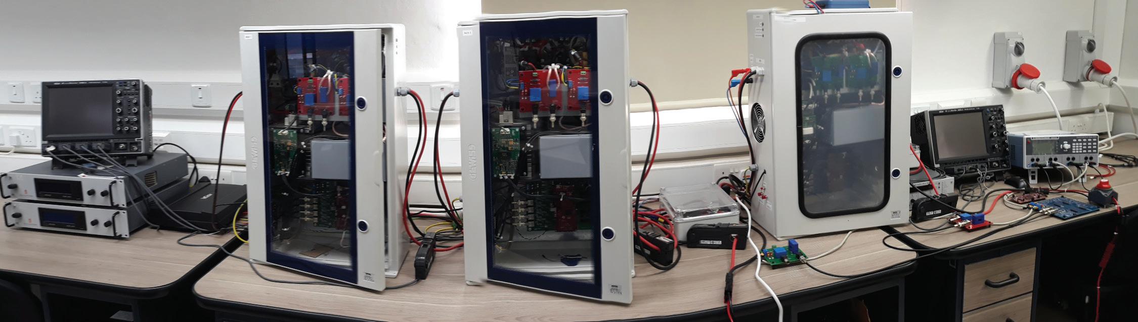
Experimental dc microgrid setups under investigation at the University of Malta. Research there has produced an innovative control system that shares current well within a dc microgrid.
POWER ELECTRONICS HANDBOOK
DC Microgrid Control System
Droop control is basically a way of equalizing current sharing among converters — it is analogous to reactive power sharing in an ac grid. Conventional droop control works by adding virtual resistance in various lines to equalize the currents. Droop control also prevents circulating currents between the power converters.
However, droop control creates voltage deviations in the microgrid, which creates a need for a voltage restoration controller within the secondary control. This voltage restoration controller is common to all power converters within the dc microgrid. It corrects the dc microgrid bus voltage to the desired value. In addition, another layer of control called tertiary control takes care of the flow of power inwards and outwards between the microgrid and the electrical grid.
Today, all these control algorithms are applied using microcontrollers, and the variables (like output current and output voltage) are sampled using ADCs. Generally, a microcontroller local to each power converter handles the primary control. Secondary control is taken care of by another microcontroller. It executes a secondary control algorithm which is common to all power converters within the dc microgrid.
A common microcontroller also generally takes care of tertiary control by monitoring and controlling the power flow or
Hierarchical Control System for dc Microgrids
current within, in, and out of the microgrid. Other higher-level control systems like Energy Management Systems (EMSs) are then employed to decide on any need to connect or disconnect to the main grid. These algorithms are generally based on the energy available in the microgrid.
Storage systems made up of battery banks integrated in the microgrid also have their higherlevel control algorithms like Battery Management Systems (BMSs) which decide when to charge and when to utilize the batteries. The power converter is controlled by the BMS, connecting the battery bank to the dc bus.
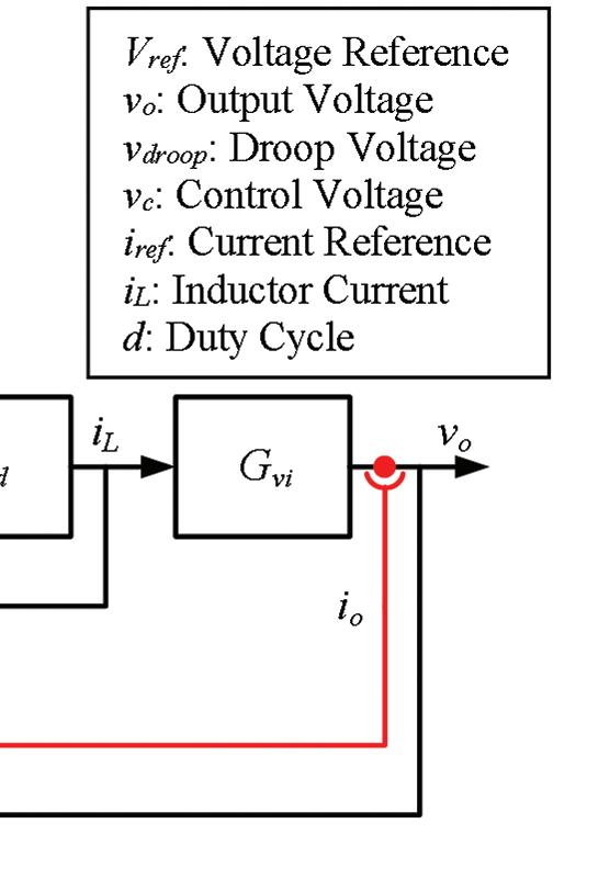
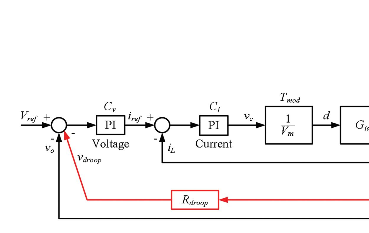
Primary control
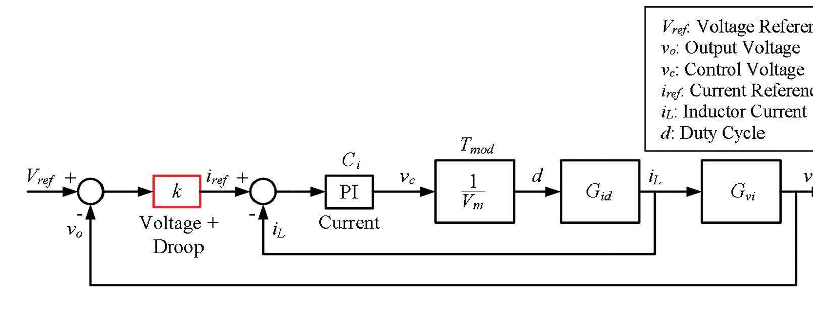
The main or primary control system for a dc/dc converter generally consists of nested current and voltage loops. When the converters are connected in parallel within a dc microgrid, droop control handles load sharing among the converters. The inner current loop controls the inductor current, while the outer voltage loop controls the converter output voltage. The inner current control
loop must be faster than the outer voltage control loop to minimize interaction between the two loops and prevent instability. Proportional Integral (PI) controllers control
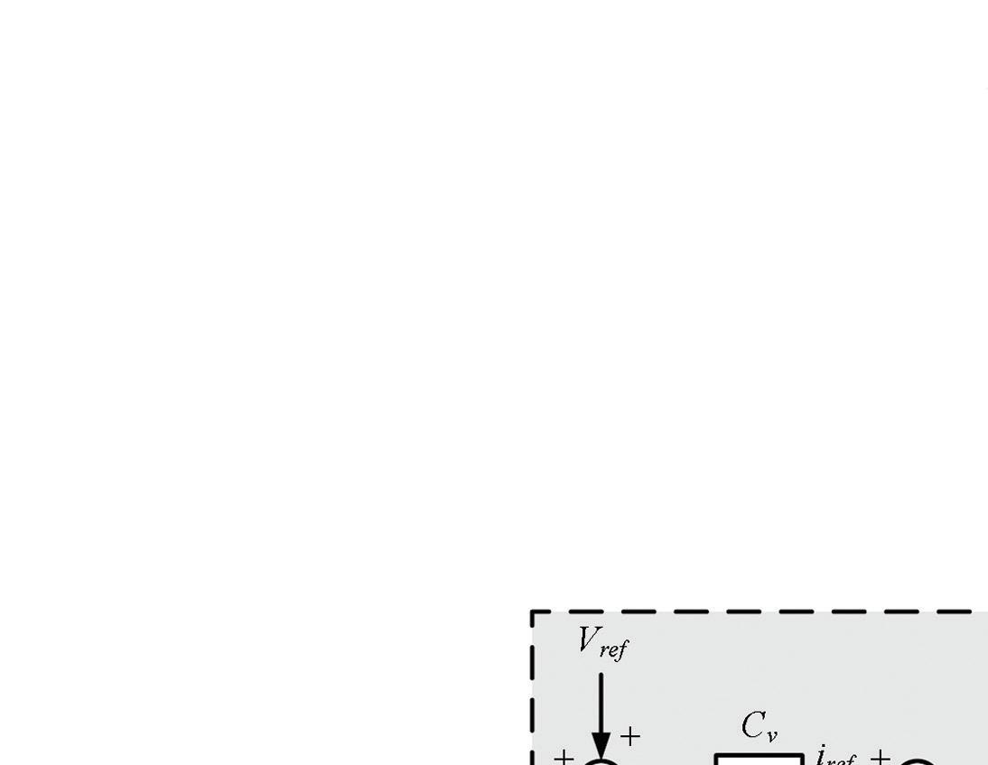
the inductor current and output voltage. The current and voltage PI controllers, C (s) and Cv(s), are of the form C(s) = Kp +(KI/s), where KP is the proportional gain term and KI is the integral gain term.
The PI controllers are designed to produce the desired response and bandwidth of the control loop. These controllers make use of the transfer functions as shown in the nearby block diagram (Figure 3), where Tmod is the transfer function representing the pulse width modulation stage, Gid(s) is the transfer function of the relationship between the duty cycle and the inductor current, and Gvi(s) is the transfer function of the relationship between the inductor current and the output voltage. These transfer functions are based on the type of power converter in use (Buck, Boost, etc.).
13 DESIGN WORLD — EE NETWORK 2 • 2023 eeworldonline.com | designworldonline.com
Figure 2. (a) Primary and Secondary Control (b) Tertiary Control
CONTROLLING DC
Figure 3. Block Diagram of the Control System with Current and Voltage Control including V-I Droop
MICROGRIDS
In many of the dc microgrid operating modes, droop control handles load sharing between parallel-connected energy source converters by adjusting converter voltage and current control loop references. As mentioned before, this method prevents circulating currents among the parallelconnected converters, which would result if there were any differences in the converter output voltages.
There are two main types of droop control methods: the impedance droop method (also referred to as V-I droop); and the admittance droop method, also referred to as I-V droop.
The V-I method can be considered the traditional droop control method. V-I droop is applied by inserting an additional loop containing a virtual resistance (Rdroop). The product of the output current and the droop virtual resistance is subtracted from the voltage reference. This causes a load-dependent deviation in the output voltage of the converter and thus a load sharing behavior between the parallel-connected
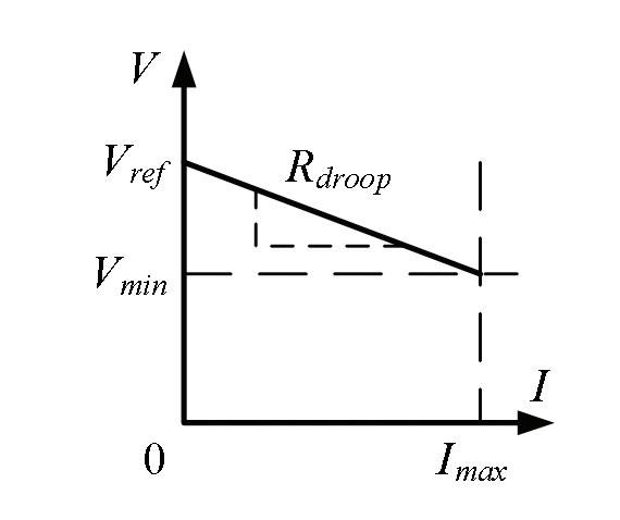
converters. The value of Rdroop is the slope of the V-I curve: Rdroop=(VrefVmin)/Imax = v /io_max where Vmin is the converter’s minimum permitted output voltage, Vref is the no-load output voltage reference, and Imax is the converter maximum current. io_max is the maximum output current and v is the maximum permissible voltage deviation calculated by v = Vref − Vmin
Therefore, the converter output voltage (vo) can be expressed as vo =Vref − Rdroopio, where io is the output current. In the case of a buck converter where the average inductor current and output current are about equal, the inductor current iL can be used instead of io in the control loop.
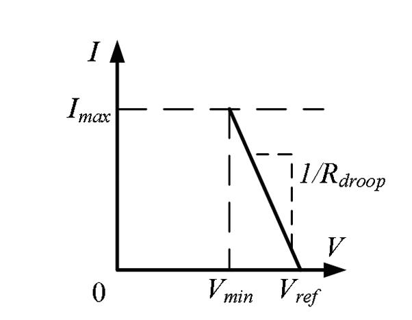
Now consider the I-V or Admittance Droop control method. Here the voltage PI controller is replaced with a multiplier term,
transfer function of the relationship between the inductor current and the output voltage.
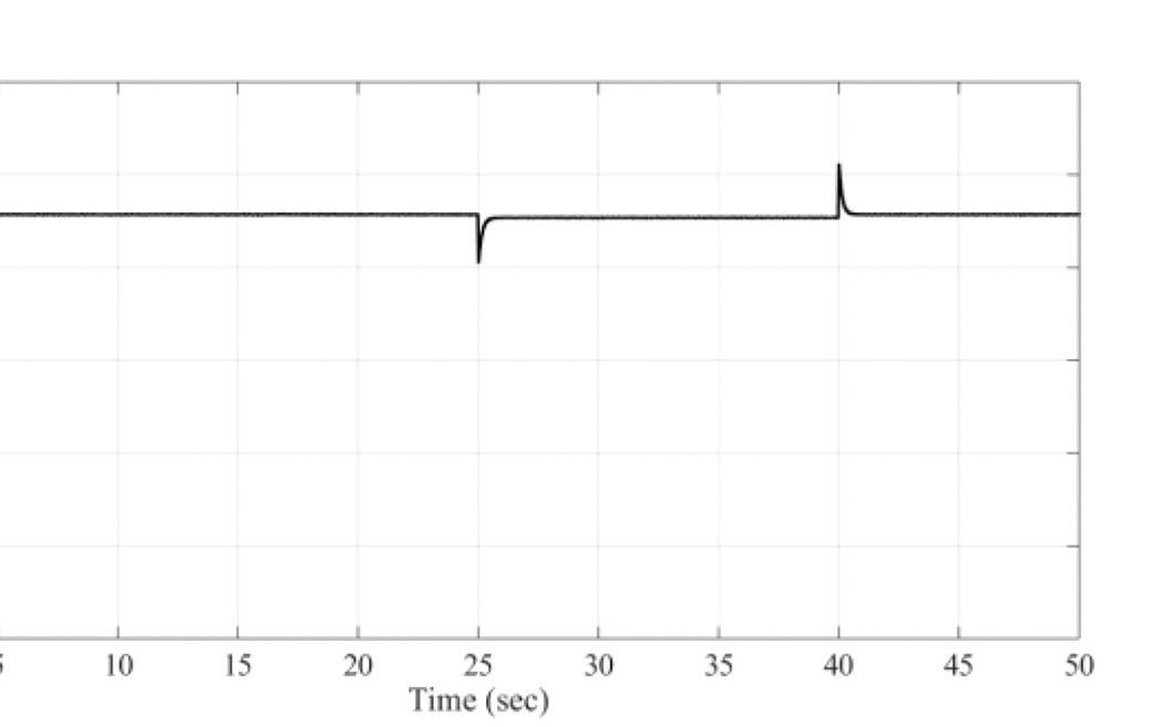
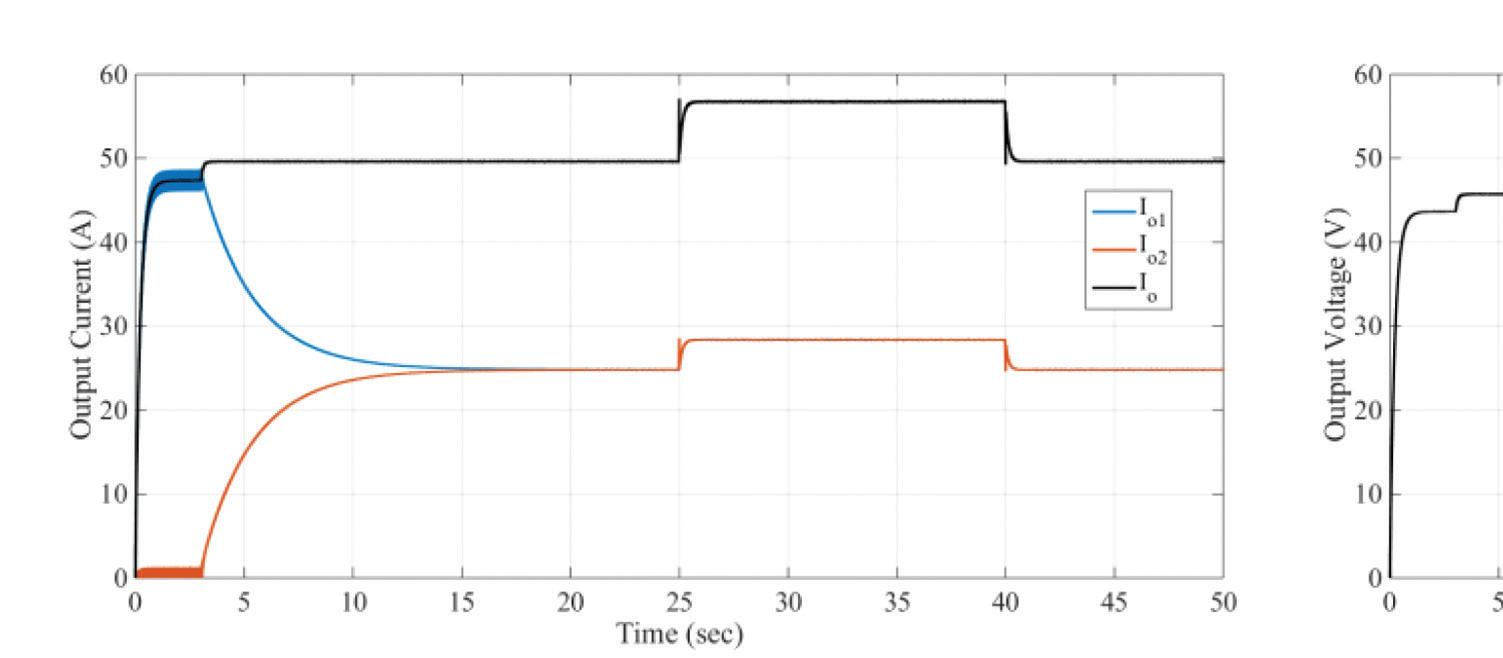
It is interesting to consider the simulation of two buck converters sharing a resistive load, Figures 6 and 7. The two converters were controlled by nested current and voltage PI controllers with a V-I droop loop. The droop resistance Rd was set to 0.092 Ω for both converters to share loads equally. The reference voltage for the voltage loop was 48 V.
Initially only one converter was switched on, supplying a resistive load of 0.92 Ω (52.08 A at 48 V for 2.5 kW). At t = 3 sec, the second converter was connected in parallel with the first and started sharing the resistive load. When the two converters operated in parallel, their respective droop loops adjusted each converter output
faster sharing, but at the expense of a bigger deviation in output voltage. Thus there’s a compromise between sharing speed and output voltage regulation.
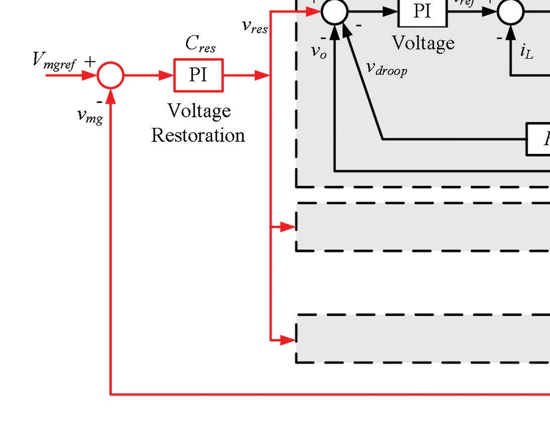
Secondary control
As mentioned before, though droop control permits the sharing of a common load among paralleled converters, it also causes an output voltage deviation that depends on the load. The voltage deviation problem can be solved with a secondary controller. This controller forms an outer control loop common to all the converters/sources in the microgrid. This control loop compares the microgrid voltage with the desired voltage, and the PI compensator of the loop generates
thus this is strictly a proportionaltype controller. The multiplier is denoted by a constant value k, which effectively is the inverse of the droop virtual resistance Rdroop, k = 1/Rdroop. The multiplier term k is multiplied to the difference between the voltage reference and the actual output voltage to obtain the current reference for the current PI controller.

The plant transfer functions that are used to design the current PI controller and used with the multiplier term k are the same transfer functions as discussed earlier; Tmod is the transfer function representing the pulse width modulation stage. Gid(s) is the transfer function of the relationship between the duty cycle and the inductor current. Gvi(s) is the
voltage to share the load current. There was a change in load at t = 25 sec, decreasing the total resistive load to 0.8 Ω and causing a 15.2% change in load current. At t = 40 sec the resistive load changed back to 0.92 Ω.
Figure 7 shows the output current from each converter (Io1 and Io2) and the total output/load current (Io), during start-up, load sharing, and the load change, while Fig. 8 shows the output voltage (Vo) during the same process. It took about 13 seconds for load sharing between the two converters to reach steady state. The total output voltage rose from about 43.64 to 45.71 V, boosting the total output current from about 47.35 to 49.6 A. Increasing the droop resistance would make for
the voltage restoration needed for the primary control loops of each converter in the microgrid.
The demanded value of the voltage restoration loop (Vmgref in figure 9) is set to the desired dc microgrid voltage. The actual dc-bus microgrid voltage (vmg) is measured and fed back to this loop. This lets the controller generate the required restoration voltage (vres). The value of vres is restricted to prevent it from exceeding the maximum allowed voltage deviation.
With the V-I droop method, the equation for the output voltage (vo) is modified to include the restoration voltage: vo =Vref +vres − Rdroopio
Tertiary control manages power flow between a microgrid and external grid networks.
14 DESIGN WORLD — EE NETWORK 2 • 2023 eeworldonline.com | designworldonline.com
Figure 4. V-I DroopGraphical Representation
Figure 5. Graphical Representation of a I-V droop
POWER ELECTRONICS HANDBOOK
Figure 6. Block Diagram of the Control System with Current and Voltage Control including I-V Droop
This power flow management helps reduce power losses and optimizes power generation sources. Level of control can have various complexities that range from managing the connection of the microgrid to the grid, according to the load requirements and power availability within the microgrid, to complete management of the various power sources to maximize their output within the microgrid.
Research on dc microgrids
Many research groups in universities are interested in dc microgrid research. For example, the Dept. of Industrial Electrical Power Conversion at the University of Malta has researched microgrids, both ac and dc systems. There, an experimental laboratorybased 5-kW dc microgrid was set up for studies on energy control algorithms and converter prototypes. The experimental dc microgrid was designed and built in-house consisting of three power converters; two buck converters used to emulate energy sources and one bidirectional converter connecting a battery storage system.
Each converter prototype was designed to be open for further research development. Research has produced an innovative control system offering good performance in load current sharing within a dc microgrid. A battery management system was also designed to control energy flow in the battery storage unit. The plan is to keep developing the dc microgrid setup and the power converter prototypes, as well as the control system.
Companies and entities with interests in research collaborations and/or sponsorships are welcome, and can contact Dr Daniel Zammit using email daniel.zammit@um.edu.mt.
The research work in the area of dc microgrid at the Faculty of Engineering was carried out as a project by engineer Daniel Zammit as part of his doctorate studies, under the guidance of Prof. Cyril Spiteri Staines, Prof. Maurice Apap, and Dr. Alexander Micallef.
References
J. M. Guerrero, J. C. Vasquez, J. Matas, L. G. de Vicuna, and M. Castilla, “Hierarchical Control of Droop-Controlled AC and DC Microgrids – A General Approach Toward Standardization,” IEEE Transactions on Industrial Electronics, vol. Vol. 58, January 2011.
T. Dragicevic, X. Lu, J. C. Vasquez, and J. M. Guerrero, “DC Microgrids – Part I: A Review of Control Strategies and Stabilization Techniques”, IEEE Transactions on Power Electronics, Vol. 31, Issue 7, pp. 4876 – 4891, July 2016.
T. Dragicevic, X. Lu, J. C. Vasquez, and J. M. Guerrero, “DC Microgrids – Part II: A Review of Power Architectures, Applications and Standardization Issues”, IEEE Transactions on Power Electronics, Vol. 31, Issue 5, pp. 3528 - 3549, May 2016.
F. Gao, Y. Gu, S. Bozhko, G. Asher, and Pat Wheeler, “Analysis of Droop Control Methods in DC Microgrids”, IEEE 2014 16th European Conference on Power Electronics and Applications (EPE’14-ECCE Europe), 26-28 August 2014, Lappeenranta, Finland.
Y. Han, X. Ning, P. Yang, and L. Xu, “Review of Power Sharing, Voltage Restoration and Stabilization Techniques in Hierarchical Controlled DC Microgrids”, IEEE Access, Vol. 7, pp. 149202 –149223, 11 October 2019.
K. M. Bhargavi, N. S. Jayalakshmi, D. N. Gaonkar, A. Shrivastava, and
V. K. Jadoun, “A Comprehensive Review on Control Techniques for Power Management of Isolated DC Microgrid System Operation”, IEEE Access, Vol. 9, pp. 32196 – 32228, 19 February 2021.
S. Ali, Z. Zheng, M. Aillerie, J. P. Sawicki, M. C. Péra, and D. Hissel, “A Review of DC Microgrid Energy Management Systems Dedicated to Residential Applications”, Energies, Vol. 14, Issue 14, 17 July 2021.
D. Zammit, C. S. Staines, M. Apap, A. Micallef, ‘Alternative Droop Control Method using a Modified Lag Compensator for Paralleled Converters in DC Microgrids’, IEEE 6th International Conference on Control, Decision and Information Technologies (CoDIT’19), Paris, France, 23-26 April 2019.
D. Zammit, C. S. Staines, M. Apap, A. Micallef, ‘Paralleling Converters in DC Microgrids with Modified Lag I-V Droop Control and Voltage Restoration’, ELECTRIMACS 2019, Salerno, Italy, 21-23 May 2019.
D. Zammit, C. S. Staines, M. Apap, A. Micallef, ‘Paralleling Converters in DC Microgrids with Modified Lag I-V Droop Control and Voltage Restoration’, Chapter in book ELECTRIMACS 2019Selected Papers - Volume 2, Springer, 2020.
D. Zammit, M. Apap, A. Micallef, C. S. Staines, ‘A Battery Management System Applied to a Bidirectional Converter for a DC Microgrid Application’, publication in process.
15 DESIGN WORLD — EE NETWORK 2 • 2023 eeworldonline.com | designworldonline.com
Figure 7: Output Currents – V-I Droop – Two Buck Converters – Load Changes 0.92Ω - 0.8Ω
Figure 8: Output Voltage – V-I Droop – Two Buck Converters – Load Changes 0.92 Ω – 0.8 Ω
Figure 9. Block Diagram of the Voltage Restoration Control Loop
CONTROLLING DC MICROGRIDS
Simplifying designs for high power density applications


High-density power module technology for FPGAs, SoCs, & ASICs makes designing easy by providing the highest power densities in the smallest spaces.
 Tony Ochoa, director of marketing,


Semiconductor integration has been proceeding at its typical breakneck pace, still following Moore’s Law. Each generation of ICs introduces new power demands with less space to satisfy them. As clever as some have been, powering solutions have always traded off power density against size and ease of use; a power module that does not force engineers to play any of these qualities against any other can go a long way to eliminating those trade-offs.
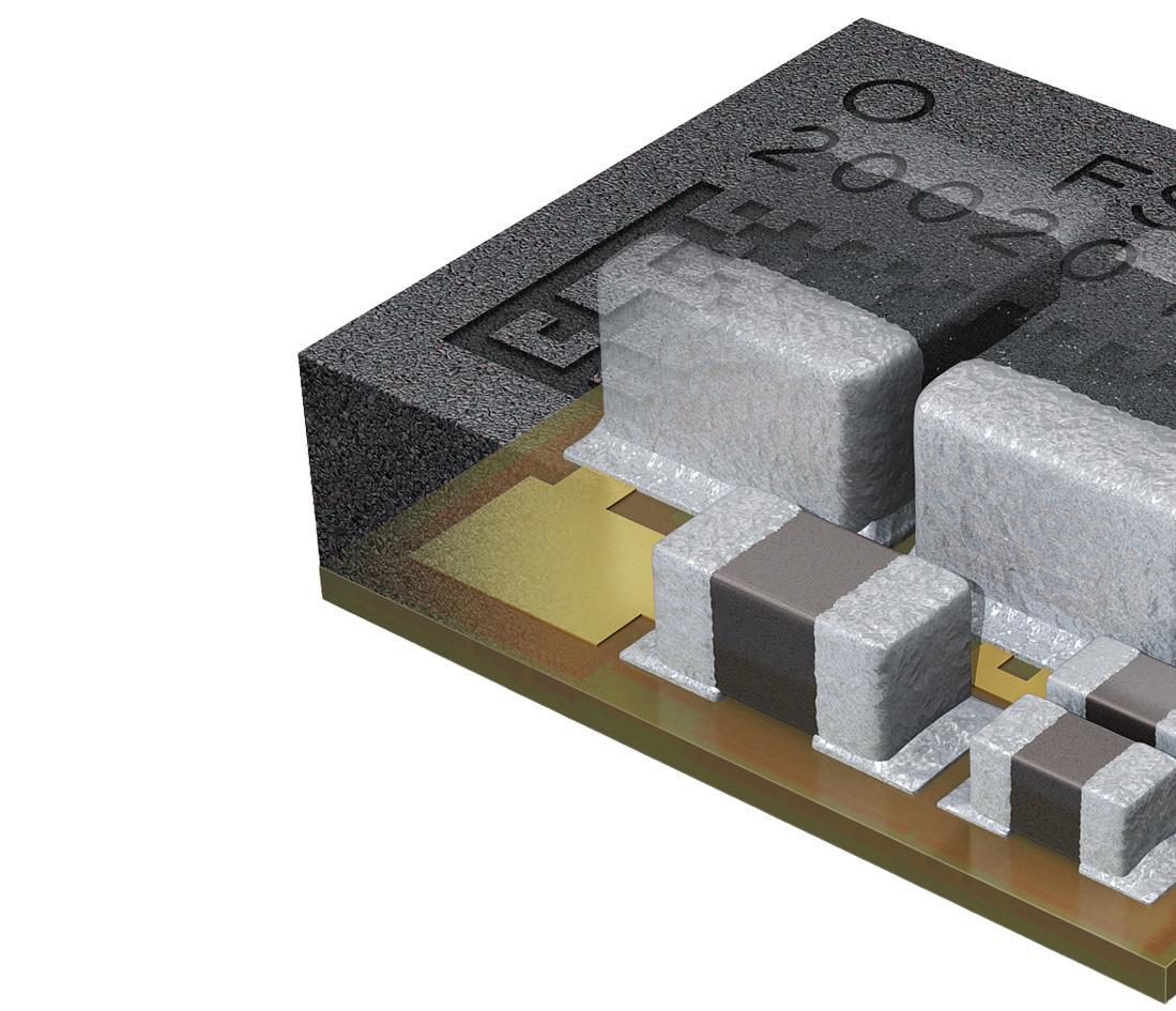
The recently announced μPOLTM power modules (see Figure 1) incorporate power circuitry built directly into a substrate to create a module that can be mounted on the front or the back of a PCB. FPGAs, SoCs, and ASICs can be mounted (as usual) nearby, and yet have shorter interconnect paths leading to better performance.
This approach has achieved 1 watt per cubic millimeter and a 15W in 49 mm3 (a typical solution with output capacitance). This technology enables the designer to achieve the highest power density in the smallest space while providing all three target benefits — power, size, and ease of use.
There are reference layouts for the most commonly used FPGAs, several Arm-based processors, and SoC (system on chip) solutions from different manufacturers. The technology behind TDK’s micropower modules is fully scalable, enabling designers to feel confident in their product roadmaps.
Ease and speed
When designing with μPOL, a designer needs only specify input capacity, output capacity, and voltage divider, then match requirements
to an available μPOL product. That is admittedly an over-simplification — but not by much. A significant amount of engineering and support resources have ensured that this technology can handle a high level of design complexity.
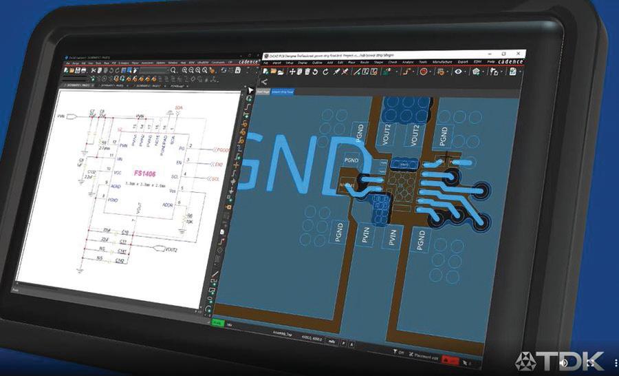
The micropower modules range from 0.6 V to 5 V output voltage, covering most designs for communication infrastructure applications, data computing, IoT, embedded vision, real-time signal processing with FPGA, robotics, and AI. Layout files that cover most of the FPGAs used in these applications are provided. Registered users can access the layouts free through Ultra Librarian, the online PCB CAD library; Cadence, Altium, Mentor, and Eagle.

16 DESIGN WORLD — EE NETWORK 2 • 2023 eeworldonline.com | designworldonline.com
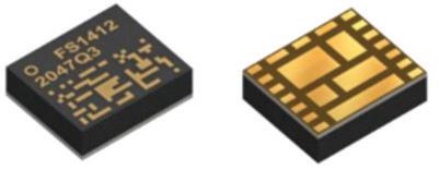
Figure 1. TDK’s μPOL power module
Figure 1. Example of an OrCAD starter design layout
µ POL DC-DC product group, TDK
POWER ELECTRONICS HANDBOOK
Figure 2. TDK’s μPOL power module product line. The maximum output voltages are dependent on the maximum output currents.
Following schematic guidelines and adhering to the suggested layouts will, in most cases, save board space, minimize the bill of materials, and allow for easy and quick design completion.
The path to power density
The micro power modules are based on TDK’s proprietary semiconductor embedded substrate (SESUB) technology, enabling 15 W power modules to be achieved in 3.3 x 3.3 x 1.5 mm packages, and 20 W+ modules in a 5.8 x 4.9 x 1.6 mm package.
Usually, high power density typically comes with thermal constraints. To overcome those
constraints, these modules integrate a chip-embedded IC, monolithic in that it comes with a DC-DC regulator, MOSFETs, and driver. A copper heat plate is added to the die, and a chip is embedded for optimal thermal flow from the die to the package, achieving as much as 4x to 8x better thermal design than competitive technologies. This assembly is incorporated directly into a four-layer, 300-micronthick substrate.
This substrate has no wire bonds. Wire bonds introduce parasitic losses, and as integration has progressed over the years, the problem has inexorably grown more severe, making it increasingly more difficult for designers to
DESIGN FOR HIGH-POWER DENSITY


applications such as drones.
space bonds and deal with the thermals. This, in turn, complicates the interconnect. The additional benefit of the chip-embedded
Because the thermal sink is positioned on the bottom of the SESUB, heat flows directly into the board, leading to substantially better thermal flow and minimizing the space necessary for the modules. With inductors, bootstrap, and Vcc capacitors are integrated, this architecture also allows the unique capability of full-rated current implementations
approach is high reliability — critical for shock and vibration prevalent in industrial and mobile
without the need for external air flow and output current deratings.
The layouts TDK has prepared for the most commonly used FPGAs and several processors include recommendations for output capacitors that will work best with each design.
Designing-in
Designers start the process by identifying each power rail’s voltage and maximum current requirement. The power map will indicate which power module is the best choice for each targeted voltage rail. A power map can additionally show where common modules can be used in multiple locations on the same design to help reduce costs through economies of scale.
Some voltages overlap values between modules. If there is a choice, the maximum current required for each power rail will determine the choice of module.
17 DESIGN WORLD — EE NETWORK 2 • 2023 eeworldonline.com | designworldonline.com TDK μPOL™ Model Output voltage A max Dimensions W rating FS1403 3.3 - 5V max 3A max 3.3x3.3x1.5mm 15W FS1404 .5 - 3.3V max 4A max 3.3x3.3x1.5mm 15W FS1406 0.6V – 2.5V max 6A max 3.3x3.3x1.5mm 15W FS1412 0.6V – 1.8V max 12A max 5.8x4.9x1.6mm ~21.5W LGA / 17PIN LGA / 22PIN
Figure 3. Example power design schematic from Ultra Librarian.
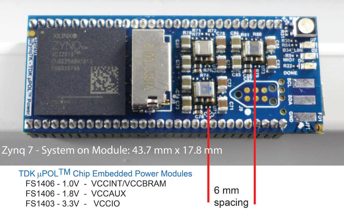
Figure 4. TDK mPOL with Xilinx SoM shows a tight power design.
When in analog mode, voltage programming for devices is not required. In this case, a simple change of a resistor is all that’s needed to set the desired output voltage accurately.
Design tools
Multiple design tools are available to engineers, making the design process easier and faster. Information found here shares links to starter power schematics and PCB layout templates in Ultra Librarian, as well as links for:
• Xilinx Artix, Spartan, and Zynq FPGAs
• Intel Cyclone, Arria, and other FPGAs
• Microchip PolarFire FPGAs and SoC FPGAs
These designs address each of the key power rails, recommend the best module for each power rail, and provide a solution tested by both TDK and the FPGA supplier.
In addition to FPGAs, there are starter power schematics for other communication processors and Ethernet chipsets:
• Marvell Armada and Cavium Octeon Arm processors
• NXP LayerScape QoriQ Arm processors
• Broadcom Ethernet controller
• Intel Ethernet controller
• Marvell Ethernet PHY
Selecting components
Once the starter schematic has been chosen, the designer must determine the required input and output capacitors. The capacitors provided in the baseline solutions address typical requirements and, though they have margin built in, still need to be thoroughly evaluated if Vin is noisy or unstable and/or if Vout supplies a high transient load.
It remains the responsibility of the designer to determine the actual capacitance needed (bulk capacitance for energy storage), the type of capacitor technology to be used, and the allowable parasitic values of the capacitors, in terms of equivalent series resistance (ESR) and equivalent series inductance (ESL). These parameters are typically dictated by the transient response requirements for di/dt (change of current per change of time).
If the design requires the support of a large di/ dt transient event, additional output capacitors may be required; the type of output capacitors may need to change based on the power distribution network’s requirements for the capacitor’s equivalent ESR and ESL.
Resistor divider values should be verified for final Vout by point-of-load measurements; the designer should adjust the resistor value if needed. Due to all the output voltage options, TDK has created support tools
that include optimized standard baseline circuits with the appropriate external passive components, schematic generation, and design layouts — minimizing board space while addressing thermal considerations.
Component design and layout
Thoughtful distribution of capacitors on the output is also essential to minimize circuit board parasitics, which can impact the supply of stored energy (current) flowing to the electrical load when needed quickly.
Connections to each power plane should be kept simple and clean to ensure no lengthy ground loops are being created, or schemes that add a high level of parasitic inductance and/or capacitance. To ensure proper performance, it is recommended that the input communication pins be electrically grounded on the PCB design if I2C or PMBUS are not used in the application.
While the power modules’ current ratings do not require additional airflow, designers still need to include enough PCB thermal vias, properly designed and located, to adequately support the system power while still maintaining thermal needs (see example below for recommended designs). For example, with effective thermal via placement on the PCB, the FS1403 at 12Vin to 5V at 3A (15W at 3.3x3.3x1.5mm) requires no airflow up to 90C board ambient.
A thorough review of the proposed final thermal via solution is recommended. It is also essential to consider the copper weight on the PCB and the number of layers. Both will impact the thermal performance.
Summary
As power demands continue to rise and space becomes ever more valuable, advances in power module technology offer intriguing design opportunities. While Moore’s Law continues to prevail, power technology is moving at a similar speed, making it easier to realize its benefits.
18 DESIGN WORLD — EE NETWORK 2 • 2023 eeworldonline.com | designworldonline.com POWER ELECTRONICS HANDBOOK
Figure 5. Layout example of the thermal vias allowing effective thermal design.
SEQUOIA & TAHOE SERIES
Precision Programmable AC and DC Sources
SEQUOIA SERIES
• Four-Quadrant Regenerative Grid Simulator with Add-On Electronic Load Option
FEATURES AND CAPABILITIES


TAHOE SERIES
• Two-Quadrant High Power AC/DC Source with Advanced Power Analyzer
• Dual Voltage ranges that support over voltage testing on 480V based systems
• 500uS time resolution for Transients


• Virtual Panels control software included


• Trigger In & Out to permit extensive coordination with external systems
• Intuitive 5” color display for ease of navigation
• Auto-paralleling for maximum flexibility with multi-chassis configurations

www.programmablepower.com 9250 Brown Deer Road, San Diego, CA 92121, USA I +1 858-458-0223
Power optimization techniques for low-power signal chain applications
Several system-level techniques are available that can make signal chains designs more power efficient and reduce system design complexity.
Low-power
signal chains
are critical when designing a batterypowered measurement system for applications such as field instruments (sensing temperature, pressure, or flow) or remote vital sign monitoring devices. Even for mains-powered systems, minimizing the environmental impact of the energy costs pushes hardware designers to improve system power efficiency. A low-power design may have indirect benefits, like smaller solution size, if enabling to reduce the number of battery cells in parallel. A further advantage of the low-power design is the lower IC die temperature due to the lower energy the system consumes, thereby extending product lifetimes.
Precision low-power signal chains are a great starting point for quickly getting a low-power hardware design done. Beyond choosing low-power components, several power optimization techniques, such as power scaling, power cycling, and duty cycling, can be implemented to reduce the system’s power consumption further. Also, design choices like appropriate resistor values or memories can be a excellent differentiator for achieving stringent lowpower targets and optimal battery life.
For example, identifying building blocks in the signal chain that can be
eliminated or powered down momentarily when certain conditions are met makes it possible to implement low-power techniques. This will require a good timing analysis1, 2, and staging or duty cycling the operation. If several building blocks are idling for the greatest portion of the time, then these can be placed into shutdown mode or directly switched off. Note that fully power cycling a device will have some implications in terms of power and timing compared to shutdown modes when available.
Once this timing is implemented correctly, significant system-level power consumption improvements can be achieved even further by minimizing the microcontroller interaction. This will require using external or internal memories to store data while the host controller is shut down.
There are some differences in how to apply power-saving techniques at the system level, depending on the type of ADC used for digitizing the sensor information, among SAR and sigma-delta, as detailed in the following sections. Also, hardware design decisions like digital comms pull-up/pulldown resistors, resistive dividers, and gain setting resistors will make a difference in the overall signal chain power consumption.
Pin naming may vary from device to device. For consistency, we will refer to AVDD for analog supply, VIO for digital supply, and VREF for reference voltage.
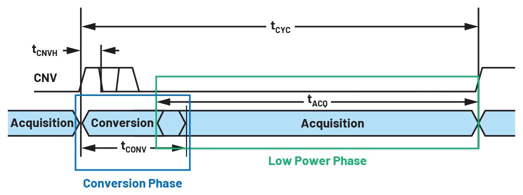
Power optimization on a SAR ADC-based signal chain SAR ADCs perform conversions on demand — that is, they toggle from sample mode to hold mode after the assertion of the CONVERSION START
 Lluis Beltran Gil, Analog Devices
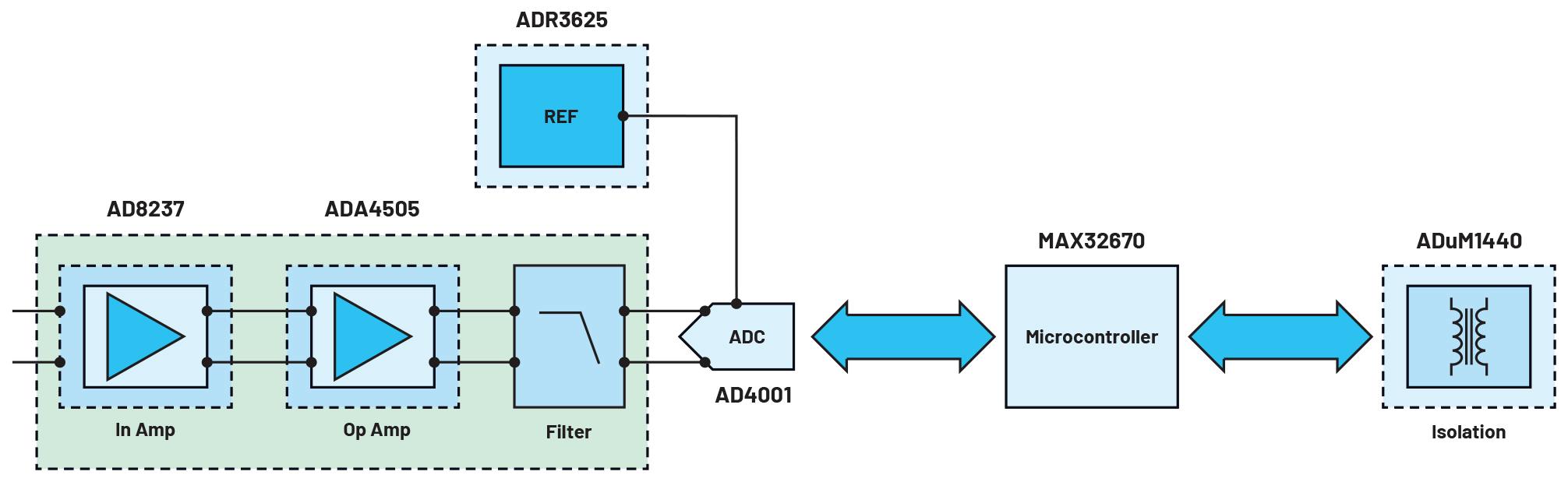
command. The conversion process starts, and once completed, it toggles back to sample mode to acquire the signal. SAR ADCs, like the AD4001 converter used in the signal chain shown in Figure 1, consume most of the power during the conversion phase, whereas consumption is minimal during the acquisition phase, as shown in Figure 2. So, despite being capable of throughputs as high as a few MSPS, power can be significantly optimized by running these converters at the minimum speed required by the application.
SAR ADC: power scaling with throughput
In many low-power applications, sensor information is not needed continuously but at much lower rates — on the order of kSPS or tens of kSPS. In these cases, power consumption of the SAR ADC can be scaled down with throughput, both for analog and digital supply rails.
Most precision SAR ADCs have an internal clock that manages the conversion process, so the conversion time (tCONV) is fixed. With tCONV being set, the lower the throughput and the longer the cycle time (tCYC), the longer the acquisition time (tACQ), the period where the ADC minimizes its power consumption. In other words, the lower the throughput rate, the lower the power consumption per sample acquired.
Conversions are triggered externally through a digital signal so that the conversion speed can be tightly controlled. A slower sampling rate results in a longer acquisition phase and, therefore, a lower average power consumption. This can be observed in
20 DESIGN WORLD — EE NETWORK 2 • 2023 eeworldonline.com | designworldonline.com
Table 1. Common Sampling Frequencies at Different End Applications
Application Common Sampling Frequency Field Instruments 60 SPs to 600 SPS Condition-Based Monitoring 1 kSPS to 10 kSPS Vital Sign Monitoring <1 kSPS POWER ELECTRONICS HANDBOOK
Figure 1. Single-channel voltage, current measurement in SAR ADC signal chain.
Equation 1:
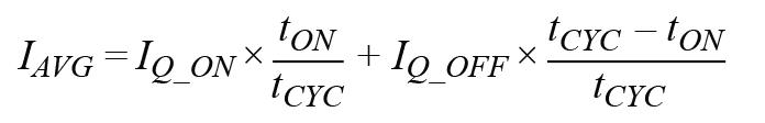
Where:
tCONV is the conversion time
tCYC is the inverse of the sampling rate
VDD is the analog supply
VIO is the digital supply
nBITS is the resolution of the ADC
tSCLK is the serial clock period time (1/fSCLK)
VREF is the reference voltage, and IREF is the current at maximum throughput (max_tput)
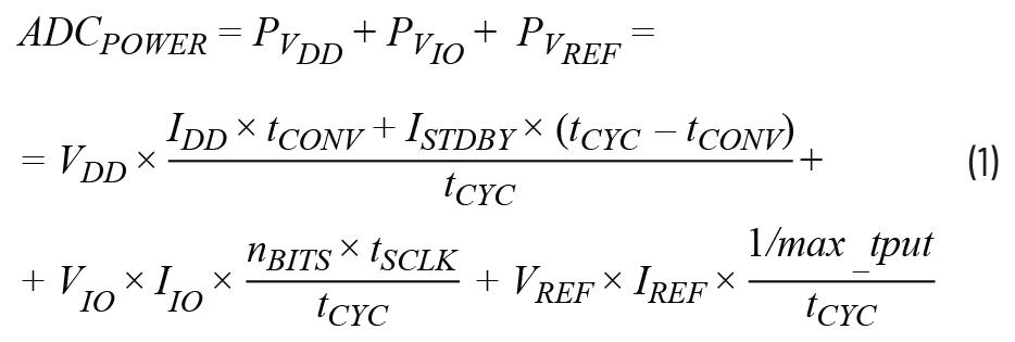
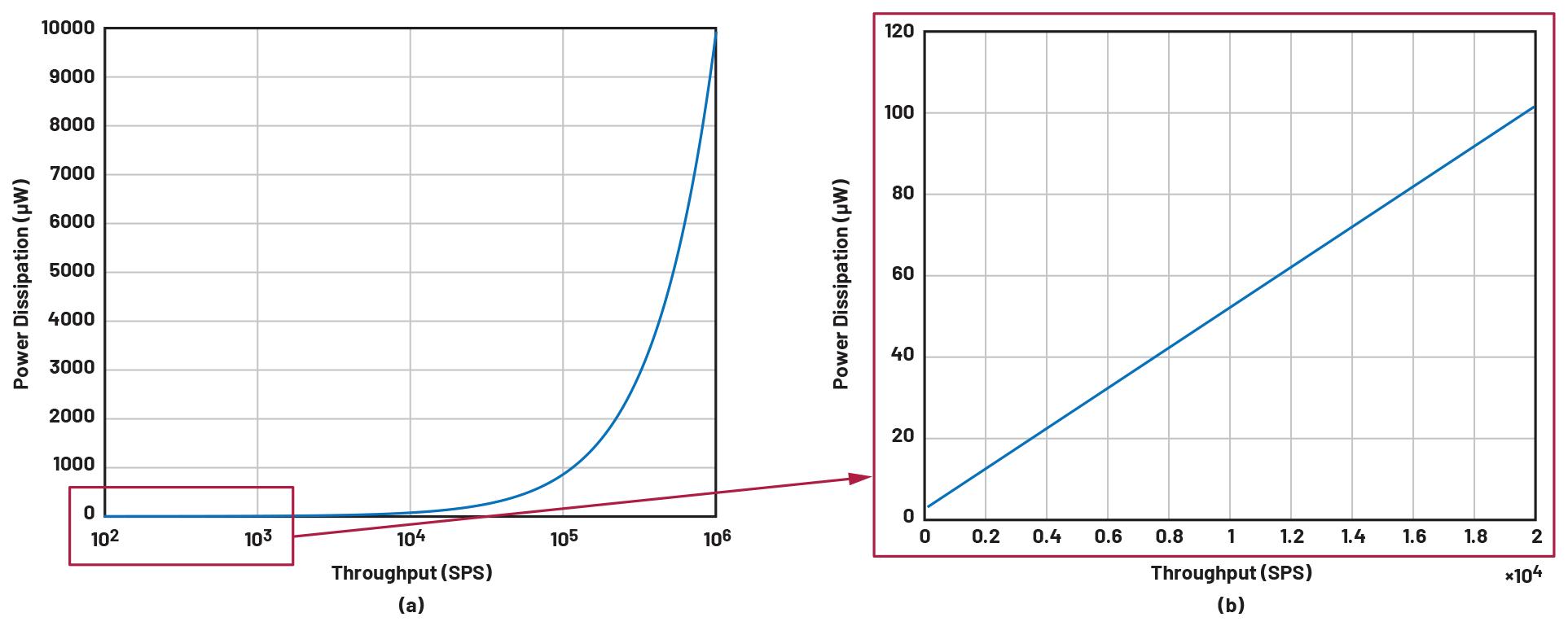
The ADC average analog power consumption will be inversely proportional to the sampling rate — according to Equation 1 and as seen graphically in Figure 4 — if tCYC is extended while tCONV remains constant.
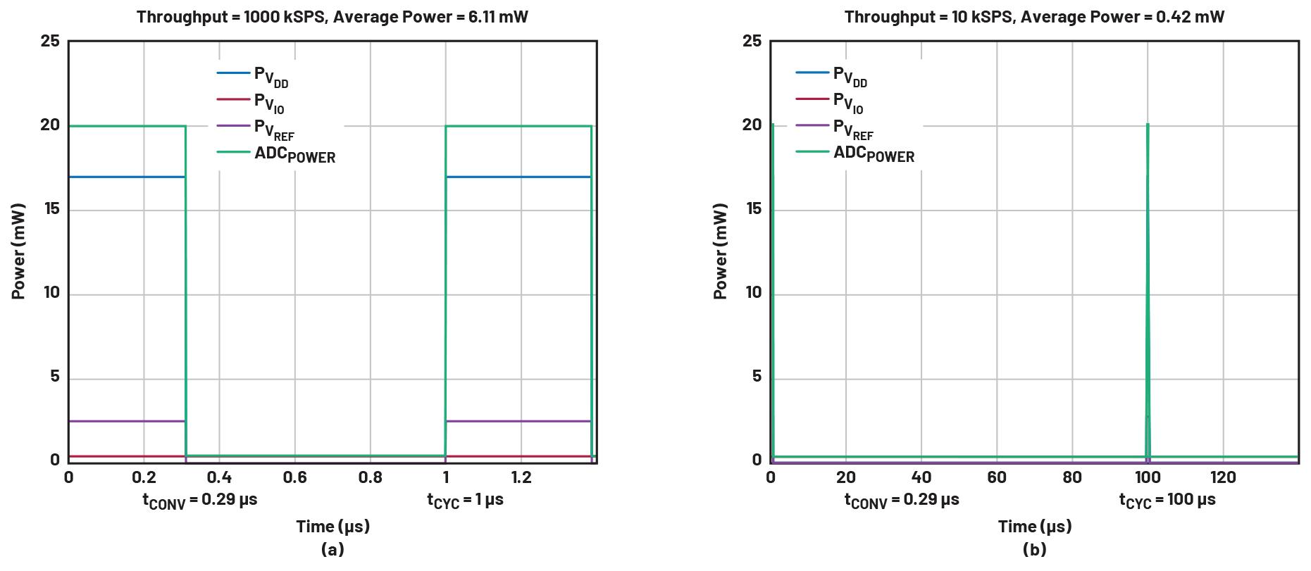
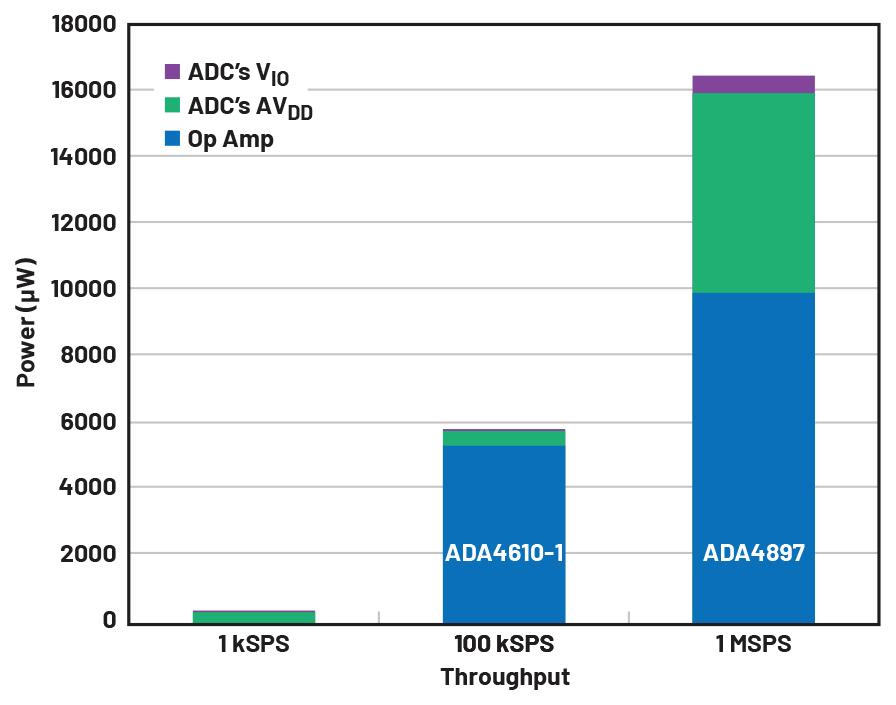
The power consumption of the ADC shown in Figure 1 is dominated by the analog supply during its conversion phase, as shown in Figure 2. For example, in a strain gauge sensing circuit, the data acquisition rate can be as low as 1 kSPS, which reduces power consumption by 20-fold compared to running the AD4001 at maximum sampling speed. A graphical representation of Equation 1 shows how the power increases exponentially with throughput, as shown in Figure 4.
Reducing the ADC sampling rate results in a longer acquisition time, which reduces the bandwidth requirements of the ADC driver amplifier, allowing a larger base of devices to choose from. Lower bandwidth amplifiers tend to have comparatively lower quiescent current. Lower ADC sampling rates lower not only ADC power consumption but also lower power requirements for companion amplifiers.
POWER OPTIMIZATION TECHNIQUES
However, selecting a lower bandwidth operational amplifier has its trade-offs. The lower bandwidth means a lower quiescent current (IQ), but it comes at the expense of increasing the voltage noise density (eN), as shown in Table 3. As a rule of thumb, lowering the quiescent current implies that the noise density increases at a ratio of 1/√IQ. However, note that the rms noise will be filtered by the adjusted bandwidth. In other words, a hardware designer might trade off power consumption (or battery life) vs. rms noise performance for the given sample rate, amplifier, and RC net bandwidth.
Furthermore, the feedback resistors used to set the operational amplifier gain will also impact power consumption: the larger these resistors are, the less power they will consume. This, again, comes with a noise trade-off as larger resistors generate more noise. A good design practice is to make the resistors as large as possible but not large enough that their contribution to the total noise is substantial. As individual noise contributions are root sum squared for obtaining total noise, following a common rule of thumb would lead us to set a maximum limit for resistor noise
(a) avg. power = 6.1113 mW at 1 μs, (b) avg. power = 0.93756 mW at 10 μs, (c) avg. power = 0.36845 mW at 1 ms.
rms of 1/3 of that of the op amp to keep their noise contribution less than 5% of the total. This would keep the op amp noise dominant. In some applications where lowfrequency input signals are sampled at low throughput rates (a few kSPS), like the ones shown in Table 1, the driver amplifier could be removed, if no signal conditioning, like a gain stage or low output impedance, is needed. In higher-speed applications, newer ADCs like the AD4000 or AD4696 families offer high input impedance (high-Z) modes that allow lower bandwidth (and lower power) amplifiers to drive the analog inputs, sometimes even eliminating the driver. Removing this op amp will also minimize total power consumption by eliminating its contribution, as indicated by the blue bar portion shown in Figure 5. This results in significant power savings compared to traditional SAR ADCs that almost always require a driver amplifier. In the case of the AD4696, a 16-channel device, this power savings is multiplied by 16 times. The reference high-Z mode feature reduces the reference input current and the overall system power consumption.
21 DESIGN WORLD — EE NETWORK 2 • 2023 eeworldonline.com | designworldonline.com
Figure 3. AD4001 SAR ADC timing diagram and power consumption during one cycle. The longer the cycle time, the lower the average power consumption:
AD4001 Throughput Rate Total Power Consumption 1 kSPS 300 μW 10 kSPS 400 μW 1 MSPS 6 mW Table 2. AD4001 Power Scales with Throughput
Figure 2. An SAR ADC timing diagram.
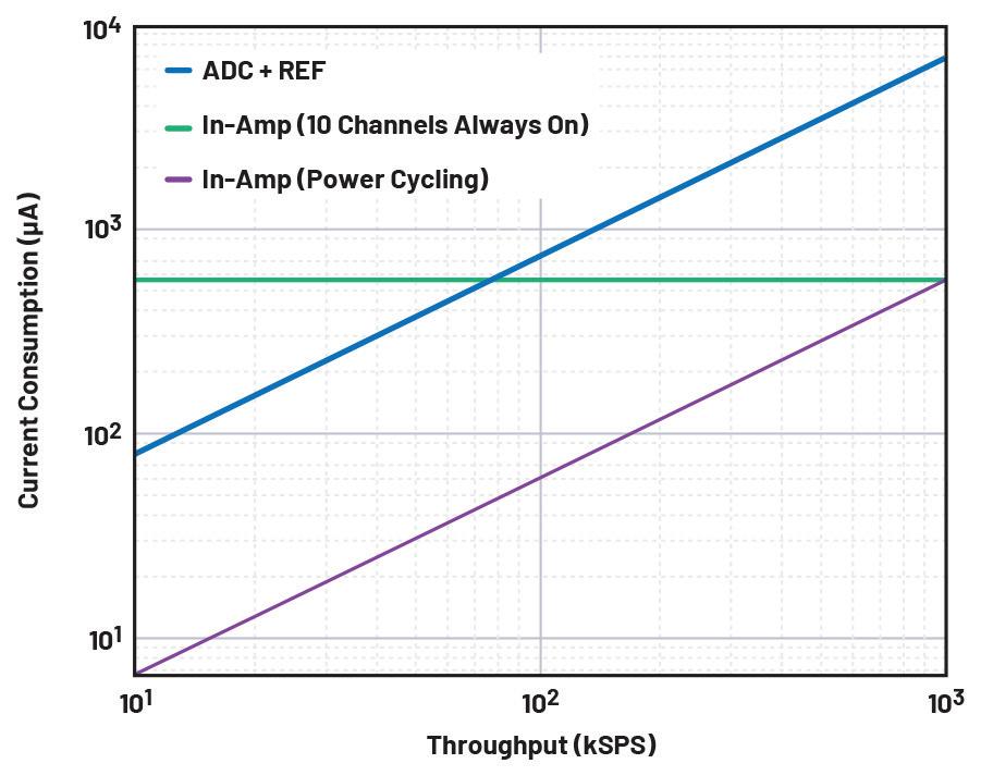
SAR ADC signal chain: AFE dynamic power scaling
As described in the previous section, SAR ADC power consumption inherently scales with sample rate, but this is not true for other signal chain components. Amplifiers and voltage references consume constant quiescent current while they are powered up. Power cycling these components between ADC samples reduces the average power consumption of the signal chain. Waiting for signals to be settled on every power cycle limits the time left for powering the system on and off. This is well explained in “What Are the Most Important Timing Factors for Low Power Precision Signal Chain Applications? Part 1”and “What Are the Most Important Timing Factors for Low Power Precision Signal Chain Applications? Part 2”(although an accurate analysis for each particular signal chain design is recommended).
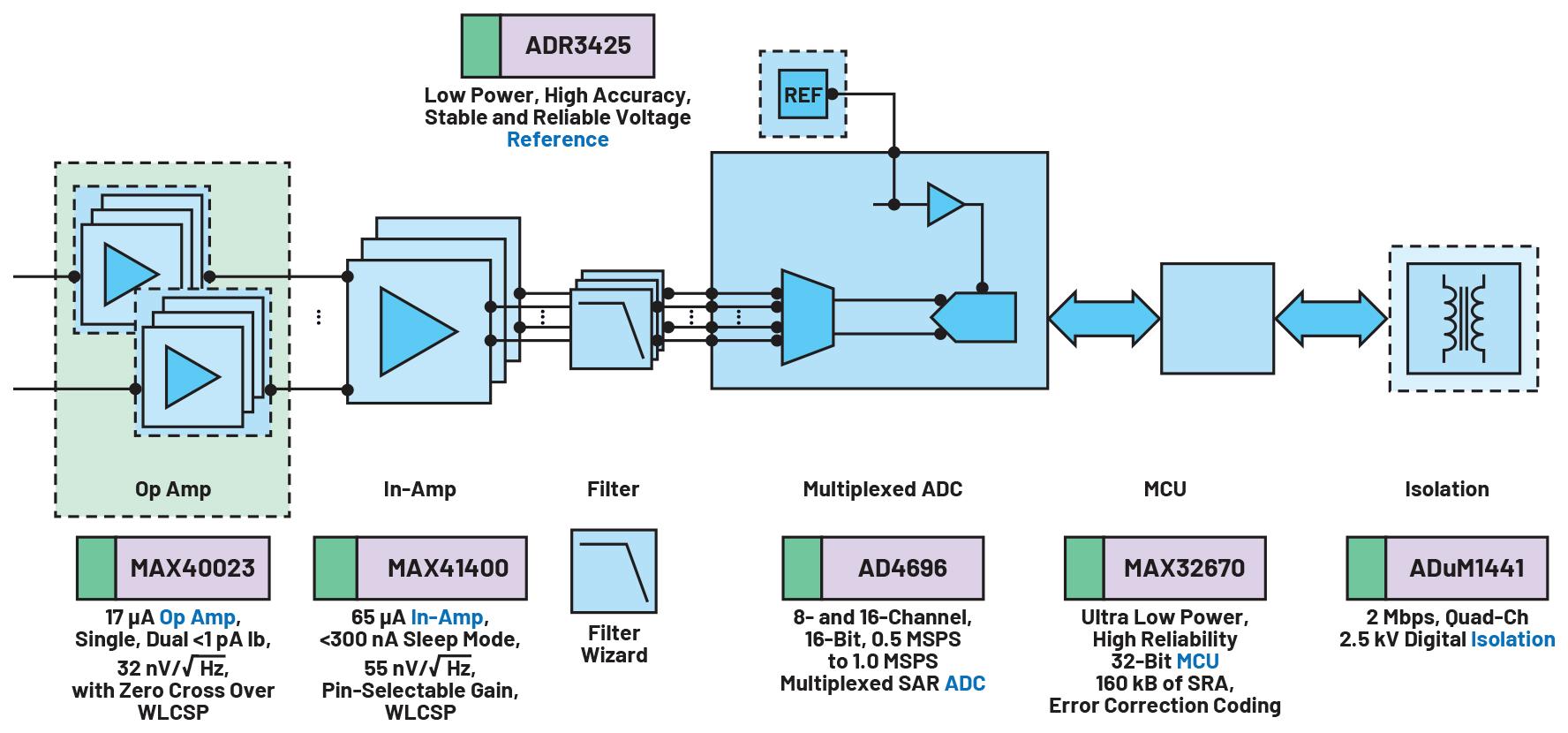
Using highly integrated ADCs, with more analog front-end (AFE) blocks on chip, enables faster power-up and power-down transitions without compromising the performance. However, in many scenarios, a design may use discrete components for optimal performance. An example is shown in Figure 6.
This signal chain is multichannel and is comprised of one MAX41400 plus one antialiasing filter per channel, feeding into a 16-channel SAR ADC (the AD4696) with an ADR3625 precision reference.
As shown in the previous section, running the ADC at the lowest acceptable throughput
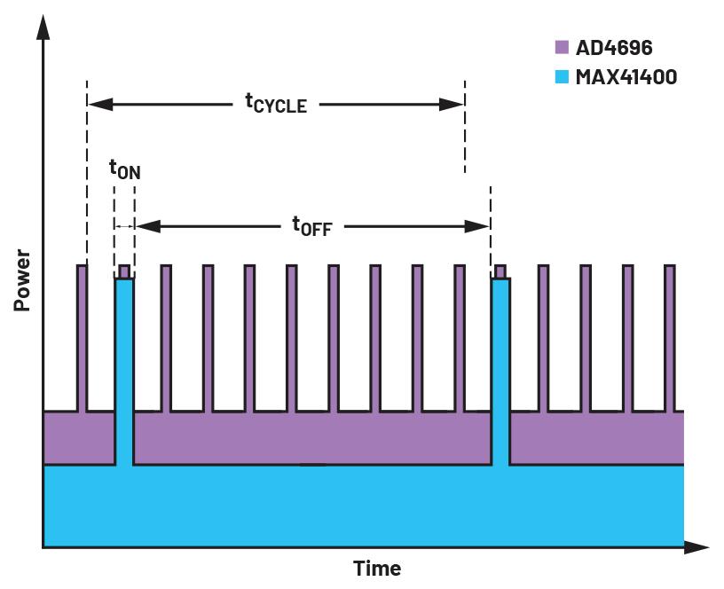
reduces its power consumption. Beyond that, if the idle time is large enough, the amplifier can be put into shutdown mode during a portion of the acquisition time, given that for a multiplexed system like this, only one amplifier needs to be powered up at a time. The frequency at which the amplifier needs to be powered up is tCYC/LSEQ, where LSEQ is the length of the sequence, which is ten in the example given in Figure 7. For example, if running conversions at 1 kSPS per channel and
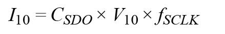
the higher the tCYC, and the lower the IAVG tON is the time during which the amplifier is turned on. When the ADC switches from the acquisition to conversion phase, the amplifier can be powered off, as extending tON longer than the minimum required does not yield any benefit. This off-time (tOFF = tCYC – tON) should be maximized for minimum power consumption, not to the extent of compromising SNR or THD. Finding the right timing will depend on the application, the devices used, and the throughput rates. In fact, tON and throughput are inversely proportional: lower throughputs lead to longer idle time, and longer idle time requires longer tON to power the amplifier back up. Based on the datasheet, the typical conversion time of the SAR ADC is 415 ns. This conversion time plus the 100 μs required to power up the amplifier after shutdown will add up to the minimum tON time. So, the average current consumption will be:
Compared to an amplifier that is always enabled, the shutdown modes and fast powerup time of the MAX41400 result in a 10× reduction in current consumption.
For a more general view, besides power savings calculated on the examples shown so far at a given throughput rate, all these equations can be represented graphically as in Figure 9, with the specifications taken from the data sheets (assuming reference and analog input high-Z mode are enabled).
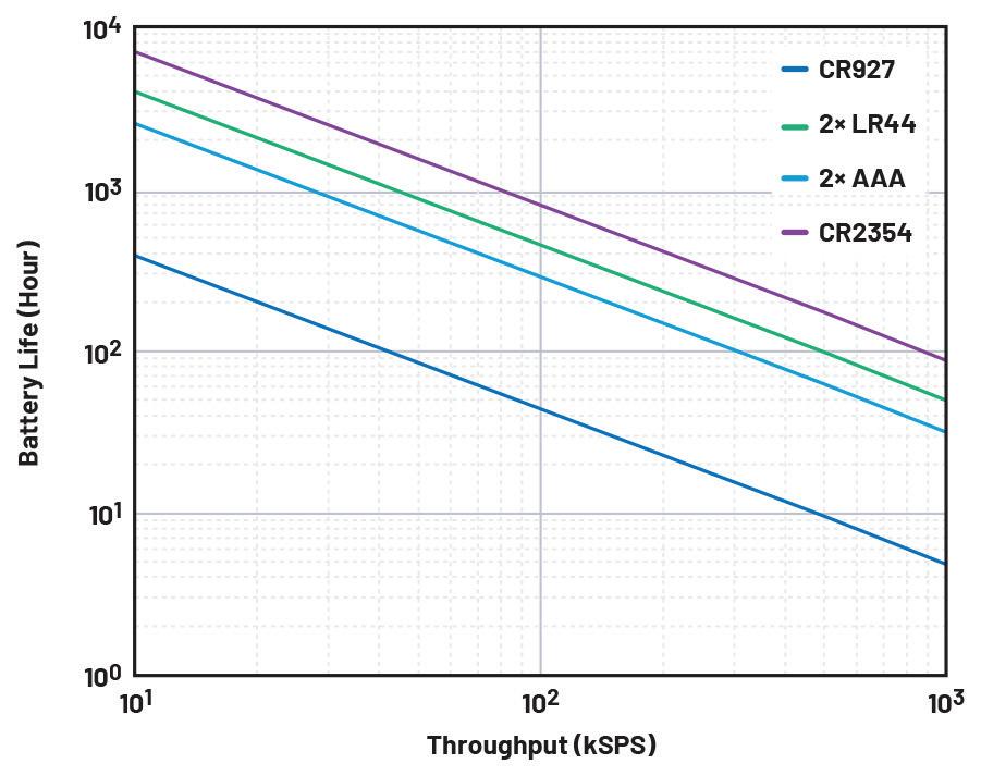
This same analysis can be done for battery life instead of power consumption by dividing the battery capacity by the average current drawn.
In this case, the relationship is inversely proportional — the lower the throughput, the longer the battery will last.
the conversion time is a maximum of 415 ns, the amplifier on each channel can be placed into shutdown mode for around 10% of the cycle time.
The quiescent current (IQ_ON) of the amplifier is 65 μA when fully powered up, but it can be reduced to 0.1 μA when placed into shutdown mode (IQ_OFF). The average current consumed (IAVG) by the amplifier can be scaled with throughput by powering it down in between samples.
Once again, the slower the throughput,
Any amplifier, even if it does not have a shutdown mode, can be power cycled. That is, powering it on and off entirely instead of entering shutdown mode. However, care must be taken. On the one hand, the wake-up time will be longer to get the amplifier ready so that the minimum tON will be longer. On the other hand, charging and discharging the decoupling capacitors repeatedly will have implications on the current drawn to charge them up every power cycle, increasing the overall power consumption compared to using shutdown modes. Also, if the sensor is still driving the amplifier inputs while the rails are not powered up, this may lead to damage if they are unprotected.
22 DESIGN WORLD — EE NETWORK 2 • 2023 eeworldonline.com | designworldonline.com
Figure 5. Power distribution per supply rail (op amp, analog, and digital rail) at various throughputs Different amplifiers were used depending on the bandwidth needs, as per Table 3.
Op Amp Bandwidth IQ eN
90 MHz 3 mA 1 nV/√Hz
16 MHz 1.6 mA 7.3 nV/√Hz
80 kHz 17 μA 32 nV/√Hz
Figure 4. (a) AD4001’s power scaling with throughput, graphical representation of (b) zooming in for the frequency range of interest—that is, under 10 kSPS.
ADA4897-1
ADA4610-1
MAX40023
POWER ELECTRONICS HANDBOOK
Table 3. Operational Amplifier Bandwidth vs. Current Consumption and Noise Performance; Bandwidth and Power Are Inversely Proportional
SAR ADC-based signal chain: digital supply power scaling
The previous section focused on reducing the analog supply power consumption, given it is the maximum contributor to the total power consumption. Reducing the throughput also has an impact on the digital power consumption as it allows the serial clock to run at a lower frequency:
Another point to note is the value of the pull-up/pull-down resistors used in the digital communication lines. These resistors ensure a proper logical level at the digital input/ output, and their value may impact the overall system power consumption. Using too low a resistor value, also known as strong pull-up, will cause a high current to flow through it. Hence, unnecessarily low values should be avoided. On the other end, if the resistance is too high, the voltage drop caused by the leakage current could result in the interpretation of an incorrect logic level. In addition, the voltage drop impacts the propagation. Designers must use the highest resistor value without compromising the voltage level (this will depend on the digital supply voltage and leakage current) or the signal integrity.
POWER OPTIMIZATION TECHNIQUES
Sigma-delta ADC-based signal chain
In the case of sigma-delta ADC-based signal chains, the power scaling concept described in previous sections is not applicable straight away. This is because conversions are not externally triggered; instead, they work from a free-running clock.They cannot remain idle for a certain period of time as a function of an external conversion start signal.
However, many sigma-delta ADCs feature standby modes that can be used if the ADC does not need to convert continuously. As in previous sections, timing considerations need to be considered as recovering the device from standby mode requires a wake-up time during which no samples can be taken.
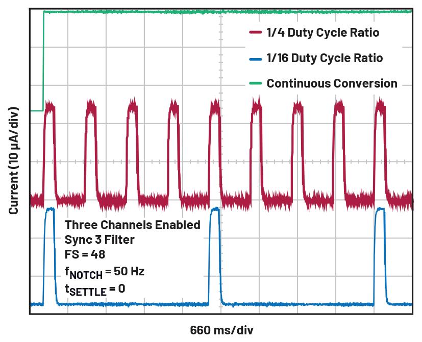
Highly integrated sigma-delta ADCs offer duty cycling and standby modes. That way, the ADC powers up and down automatically without the need to interact with the host every cycle. The AD4130 offers two modes, 1/4 and 1/16, which means it is active during 1/4
or 1/16 of the time. That leads to significant power reduction compared to continuous conversion mode, as shown in Figure 10. Depending on the required throughput rate, techniques for optimizing power consumption can be either using one of the duty cycling modes or just putting the part into standby mode for a given period. Indeed, the AD4130 has many operating modes that may impact power consumption of the ADC. The active functional model in ACE6 shows the power consumption and the expected battery life for the selected ADC configuration.
Sigma-Delta ADC-based signal chain: AFE dynamic power scaling with duty cycle
Just as with the SAR ADC-based signal chain, a sigma-delta-based signal chain can take advantage of the duty cycle to power down certain blocks when the ADC is placed into a low-power state (Figure 10). That would allow AFE power savings similar to the ones shown in Figure 9.
Sensor excitation
A complete solution provides the core converter, the internal programmable gain
amplifier, and sensor biasing and excitation (selectable current source and precision voltage reference). This integration has implications in terms of ease of use, size, and optimization on biasing, timing, or power cycling among the different building blocks. The ADC reduces the overall system power consumption by
23 DESIGN WORLD — EE NETWORK 2 • 2023 eeworldonline.com | designworldonline.com
Figure 6. A multichannel measurement signal chain.
Battery Capacity (mAh) CR927 30 2x LR44 158 2x AAA 1000 CR2354 560
Figure 7. Power cycling the MAX41400 in a multichannel multiplexed application, based on the AD4696 ADC (assuming only ten channels are used for easier visualization).
Figure 8. Signal chain power consumption vs. throughput, with and without power cycling at the front end.
Figure 9. Battery life extends with power cycling/scaling.
Table 4. Batteries’ Capacity
housing all these blocks on chip. Furthermore, it simplifies the design cycle thanks to its flexibility in many different platforms like RTD, thermistor, or bridge sensors, to name a few. It also reduces the BOM count and the need for several power supply rails.
Other power optimization techniques
Throughout this article, several ways to minimize the signal chain power consumption have been presented. However, one portion of the signal chain has not been considered yet is the host controller. If the controller is powered up all the time because it needs to read and post-process data from the ADC, it will sink a good portion of the power. Placing the controller into sleep mode while not in use will help achieve extra power savings.
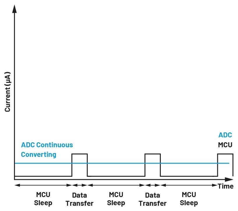
ADCs with on-chip FIFO
If the application does not need real-time data but must read data points at a much lower rate, ADCs with on-chip FIFO might play a role. The AD4130 incorporates such a block, and this FIFO can store up to 256 conversions, so if the output data rate (ODR) is, for example, 2.4 kSPS, instead of reading every 416 μs, the microcontroller can be put to sleep mode and wake up every 100 ms to read the whole data memory in one go (see
the Data Transfer section in Figure 11). In other words, having an ADC with memory that stores up to the latest 256 samples also enables power cycling of the microcontroller, thereby drastically reducing the overall system power consumption.
Streaming ADC data to memory through Direct Memory Access (DMA)
An alternative for ADCs that do not include on-chip FIFO would be to use the direct memory access (DMA) available in most microcontrollers. DMA enables the passing of data directly from a peripheral (in this case, the SPI) to memory (SRAM) without CPU intervention or interrupts for every single ADC sample received. The chosen microcontroller will have a direct impact on achievable power savings. In many cases, the microcontroller can stay in sleep mode most of the time and trigger an event only when an ADC sample is received. This event will then briefly alert the DMA to start performing the SPI transactions and to return to sleep after that, thus minimizing the microcontroller power consumption compared to having the CPU fully awake for the whole SPI transaction. Note that using the DMA is only applicable if the format of the ADC data matches the destination memory. For most microcontrollers, the DMA can be easily used only when the ADC data is 16 or 32 bits long.
Interrupt-driven programming
Many low-power applications do not require the recording and processing of every single data point but rather monitoring that the magnitude sensed is within certain thresholds. Traditionally, to do this, the host controller needed to be constantly awake to read each ADC sample and decide if the value was acceptable or not. Consequently, it would trigger an interrupt routine if need be.
Thresholds can be programmed such that a GPIO pin asserts only if the ADC output code is out of the user-defined bounds. This way, the host controller can stay in sleep mode most of the time and only wake up when the GPIO asserts, minimizing its power consumption, given it will only be active when it is necessary to perform an action.
Conclusion
When designing a battery-powered measurement system for applications such as portable field instruments, condition monitoring, or vital sign measurements (VSM), low-power signal chains are ideal for achieving poweroptimized solutions. Analog Devices’ precision low-power signal chains ease the journey for
designers building low-power measurement solutions, which offer the optimal combination of precision amplifiers, voltage references, ADCs, and isolation products. In these signal chains, power consumption is optimized while keeping noise performance, size, and ease of use as key vectors. These signal chains come in different flavors: single-channel, discrete multichannel (multiplexed), fully integrated multichannel solutions, and ready-to-go poweroptimized designs, offering an excellent starting point for low-power design.
References
Padraic O’Reilly. “What Are the Most Important Timing Factors for Low Power Precision Signal Chain Applications? Part 1.” Analog Dialogue, Vol. 56, No. 3, August 2022.
Padraic O’Reilly. “What Are the Most Important Timing Factors for Low Power Precision Signal Chain Applications? Part 2.” Analog Dialogue, Vol. 56, No. 3, August 2022.
The Data Conversion Handbook. Analog Devices, Inc., 2005.
Michael Clifford. “Fundamental Principles Behind the Sigma-Delta ADC Topology: Part 1.” Analog Devices, Inc., January 2016.
Bruce Pepitas. “Introduction to Dynamic Power Scaling.” Analog Devices, Inc., January 2016.
Analysis | Control | Evaluation (ACE) Software. Analog Devices, Inc.
Brandon Hurst. “How to Accelerate Peripheral Monitoring in Low Power Wearables with DMA.” Analog Dialogue, Vol. 56, No. 1, January 2022.
Maithil Pachchigar and Alan Walsh. “NextGeneration SAR ADC Addresses Pain Points of Precision Data Acquisition Signal Chain Design.” Analog Dialogue, Vol. 50, No. 4, December 2016.
Sanjay Rajasekhar and Arvind Shankar. “How to Leverage Input High-Z Technology to Reduce Solution Power and Size.” Analog Devices, July 2022.
24 DESIGN WORLD — EE NETWORK 2 • 2023 eeworldonline.com | designworldonline.com POWER ELECTRONICS HANDBOOK
AD4130 Power Mode Typical Current Consumption Continuous Conversion 32 μA Duty Cycling 5 μA Shutdown Mode 0.5 μA
Figure 11. Microcontroller power reduction by using the ADC’s onchip FIFO.
Table
5.
AD4130 Current Consumption for Each Power Mode
Figure 10. AD4130 current consumption under different modes of operation: continuous conversion, 1/4 duty cycle, and 1/16 duty cycle.
REGISTRATION IS NOW OPEN
A better way to handle
dc-dc converter hold-up times
Converters with built-in holdup circuitry reduce the size and requirements for input capacitors.
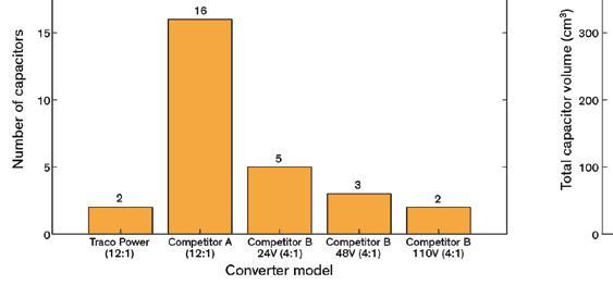
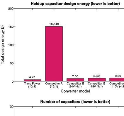
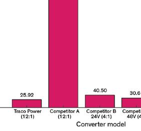
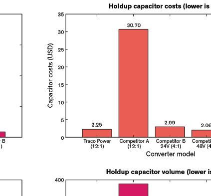
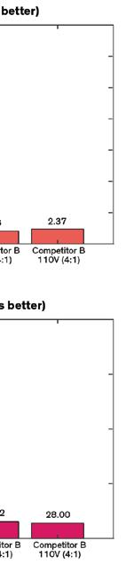
DC-DC converters are generally designed to maintain their output despite brief interruptions of their input power. The duration of this output hold-up often is set by the value of an external capacitor connected across the converter input terminals. However, some types of converters now feature a dedicated holdup capacitor connection (Bus pin). This scheme can save up to 93% on external capacitor costs while reducing their volume by up to 93% as well.
A case study helps illustrate the benefits of the approach. Consider as an example the power supply for a passenger information system as used on (light) rail vehicles. Light rail applications can experience long supply voltage interruptions. The EN 50155 standard for railway applications — rolling stock spells out requirements for the operation, design, and testing of electronic equipment on rail vehicles. Thanks to its comprehensive consideration of “harsh” environmental conditions, the EN 50155 is often considered for design of ruggedized industrial applications. This includes continued operation during an interruption of the supply voltage for a duration of up to 20 msec, a common occurrence in battery powered applications.
During the interruption, the input may be shorted. Power must come from an (external) hold-up capacitor bank. The design of the holdup circuit and the dimensioning of the capacitor bank are important parts of the overall application design process.
Light rail passenger information systems typically include a small screen, a field computer and networking peripherals such as industrial ethernet and/or IEEE 802.11 wireless communication. A 40-W power supply is typically adequate for handling these demands. Important electrical requirements of the dc supply include providing the industry standard 24, 48, 96, and 110-V battery system voltages as well as high and low input voltage limits, a maximum transient input voltage, and the maximum duration of an interruption the supply can handle.
We’ll consider three scenarios involving three different holdup circuits. Scenario A presents the use of a supply which also contains a dedicated holdup capacitor connection. Scenario B uses a comparable 12:1
Dr. André Buffing, L. Dinkelmann, Traco Power
Key requirements of the power circuit for a passenger information system on light (rail) vehicles.
Dimensioning and design of the capacitor bank used to ride through supply voltage interruptions.
26 DESIGN WORLD — EE NETWORK 2 • 2023 eeworldonline.com | designworldonline.com POWER
ELECTRONICS HANDBOOK
Scenario A Scenario B Scenario C Application Passenger information system Design channels Single Multiple Holdup connection Dedicated With input Power converter TEP 40UIR Competitor A Competitor B Output power Pnom 40 W 40 W 40 W 40 W 40 W Lowest nominal input voltage Vnom,min 24 V 24 V 24 V 48 V 96 V Highest nominal input voltage Vnom,max 110 V 110 V 24 V 48 V 110 V Maximum (transient) input voltage Vin,max 154 V 154 V 154 V 154 V 154 V Output voltage Vout,max 24 V 24 V 24 V 24 V 24 V Duration of interruption Tholdup 20ms 20ms 20ms 20ms 20ms Scenario A Scenario B Scenario C Worse-case power-conversion efficiency ηwc 90% Minimum required holdup capacitance Ch.min 10’641 μF 7’234 μf 5’349 μF 1’335 μF 0.358 μF Maximum UVLO threshold Vuvlo 14.4 V 14.4 V 8.8V 17.5 V 42 V Capacitor rated voltage Vh,rated 25 V 200 V 50 V 100 V 200 C Capacitor Nichicon UPW1E682 MHD Nichicon UPW2C471 MRD Nichicon UPW1H12 2MHD6 Nichicon UPW2A5 61MHD Nichicon UPW2C2 21MRD6 Number of capacitors in parallel 2 16 5 3 2 Cost per capacitor $1.12 $1.91 $0.60 $0.69 $1.19 Total capacitor volume (box) 26 cm3 387 cm3 41 cm3 31 cm3 28 cm3 Total capacitor costs $2.25 30.70 $2.99 $2.06 $2.37 Comparison of the design energy, capacitor costs, number of capacitors and volume for all three scenarios.
ultra-wide input voltage range product which does not include a dedicated lowvoltage holdup capacitor circuit. Scenario C presents a reference design based on a state-of-the-art 4:1 wide input voltage range dc-dc converter which also does not incorporate a dedicated holdup capacitor connection.
The sizing of the holdup capacitor bank differs for all three scenarios. In scenario A, normal operation charges the holdup capacitor through an internal circuit of the dc-dc converter. If there is an interruption in the supply voltage, the dedicated holdup circuit automatically switches the power over from the input clamps to the external holdup capacitor. A diode in the input of the dc-dc converter prevents an accidental reversal of the supply voltage from damaging the converter and prevents the hold-up capacitor bank from discharging into the main power source.
The minimum holdup capacitance C1 = Ch,min is calculated according to
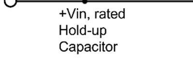
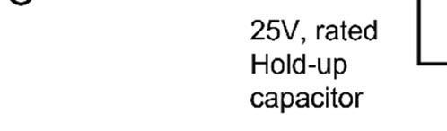
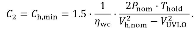
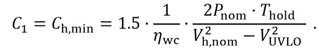
feature, Vh,nom is a constant 21.4 V for all nominal input voltages during normal operation. This allows the application designer to use low-voltage capacitors for the holdup energy storage with a Vc1,rated rated voltage of 25 V. The fact that Vc1,rated is only slightly above Vh,nom underlines the effectiveness of the design. The holdup time can be reached even if an interruption occurs at the lowest nominal voltage, as required by the EN 50155.
Scenario B employs a dc-dc converter input circuit that contains the holdup capacitor, two diodes, and a resistor R1. During normal operation, the holdup capacitor charges via the resistor. In case of a supply voltage interruption, the holdup capacitor supplies its stored energy to the dc-dc converter via one of the diodes. The other diode prevents converter damage in case of an accidental reversal of the input voltage.
The selection of R1 presents a tradeoff between limiting the inrush current and minimizing the (re-)charge time of the capacitor bank. The minimum holdup capacitance C2 = Ch,min is calculated according to
a high input voltage presents a significant drawback for the conventional design. To provide a cushion for safe operation, a Vh,rated of 200 V might be specified.
Turning to scenario 3, dc-dc converters with a 12:1 ultra-wide input voltage range are still relatively new on the market. So we will consider a state-of-the-art design using a dc-dc converter with a 4:1 wide input voltage range. The limited input voltage range forces the use three different dc-dc converters, one for each nominal system voltage. But the design methodology for the holdup circuits is virtually identical to that in scenario B.
Test results
Tests reveal that thanks to its dedicated holdup capacitor connection, the scenario A converter (Traco Power TEP 40UIR) can employ an external holdup capacitor 93% smaller than that necessary in scenario B, along with a similar reduction in holdup capacitor costs. Compared to scenario C--a 4:1 wide input voltage range dc-dc converter — scenario A capacitor volume can be up to 36% smaller and 25% less expensive while simultaneously reducing the number of assembly variants from three to just one.
While the requirements and design decisions in this comparison have been simplified for clarity, they accurately reflect the core engineering challenges of overcoming short interruptions of the dc supply voltages. Nevertheless, it is worth noting that these scenarios present theoretical considerations based on ideal operating conditions and ideal component qualities.
where the variables represent the same entities as in equation one. Because there is no dedicated holdup circuit, the holdup capacitor voltage Vh,nom follows the input voltage, thus Vh,nom = Vnom,min = 24 V. The capacitor bank must be designed for the maximum (transient) input voltage of Vh,rated ≥Vin,max ≥154 V. The need to handle
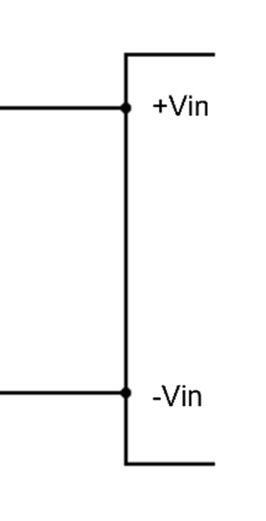
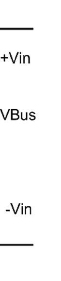
Of course, real applications require additional input filters, thermal considerations, and so forth. Compliance guidelines and (technical) regulations may also affect the design. Tolerances, aging, and environmental conditions may require their own risk management measures. Different circuit variants (e.g., with active changeover of the input voltage) require different design methodologies.
where wc = dc-dc converter power conversion efficiency at full load, Vuvlo = the lowest input voltage at which the converter can operate properly, Vh,nom = the charge voltage of the holdup capacitance during normal operation, Pnom = dc-dc converter nominal power, and Thold = holdup time, seconds. A factor of 1.5 is included to account for component tolerances and other non-idealities.
Thanks to the extended holdup
All in all, when using a converter like that in scenario A, such as the Traco Power TEP 40UIR dc-dc converter, the application engineer can save up to 93% on holdup capacitor costs and reduce the volume of the holdup capacitors by up to 93% compared to an approach without a dedicated holdup circuit. And developers can reduce engineering, certification, testing, assembly, retooling, stocking, maintenance, and support
as well.
References
Traco Power, www.tracopower.com
EN 50155- Railway applications - Rolling stock - Electronic equipment, www.en-standard.eu/bsen-50155-2021-railway-applications-rolling-stockelectronic-equipment/TEP 40UIR dc/dc converter, www.tracopower.com/series/tep-40uir
CONVERTER HOLD-UP TIMES 27 DESIGN WORLD — EE NETWORK 2 • 2023 eeworldonline.com | designworldonline.com
costs
Example, no dedicated hold-up
Example, no dedicated hold-up cap
Simplified circuit diagram of the holdup circuit when using a dc-dc converter with a dedicated holdup capacitor connection (“Bus pin”).
Simplified circuit diagram illustrating the connection of the holdup capacitor bank when the dc-dc converter does not feature a dedicated holdup circuit.
Circuit boards don’t behave the way you think they do
Circuit designers increasingly must concentrate on the design of transmission lines, or the “spaces” between traces, instead of the “wires” on a circuit board.
Whenit comes to the design of printed circuit boards, the industry focus has been on the movement of charges in the traces. The fact that design engineers don’t always appreciate is that current flows only because electric fields are moving. More to the point, the fields carry the energy, not the displacement current. My apologies to EM physicists for oversimplifying these concepts, but this approach will boost the chances of success for most designs.
Engineering teams worldwide face increasingly difficult challenges in designing electronic products and realizing good signal integrity and compliance. Today, it’s common to expect that a design will fail EMC testing not just once but three, four, maybe even five times. Each time the design is retested, there is little confidence in success.
This cycle is expensive in both the time for a redesign and the cost of urgently refabricating the new PCB and assembly. The numbers add up quickly. The expense and delay in product certification are seldom budgeted or scheduled and directly affect the bottom line and the customers waiting for the product. Instead of designing the next big thing, teams are trying to fix the current one. Billions of dollars are lost each year designing products that most likely won’t work.
What is wrong here? This “Billion-dollar mistake” is rooted in the misunderstanding of the nature of electromagnetic energy.
One drawing is to blame: It depicts a simple on/off switch controlling a light bulb powered by a battery. The perspective from this simple drawing has set the tone and philosophy for PCB design (Figure 1).
The focus has been on the current flowing in the conductor, and the result has been a steady rise in EMC failures as IC geometries grew smaller and switching frequencies rose. From this diagram, the wires started to be called “conductors” because the energy flowed in the wires. The current flowed in a loop, so the idea that this was a “circuit” was born.
But not so fast: If the energy was instantly seen at the load when the switch closed, there would be no signal integrity or EMC problems. There would also be no such thing as radio because the same energy in an electrical system is also in the air. Also, there would be no life on earth, as the light from the sun would not travel here without wires.
News flash: The wires are not conductors; they form boundaries, much like the banks of a stream. The energy does not flow through the wires; it travels in the space between them. This space, or dielectric, is the conductor. The energy is carried by the moving
EM fields in the dielectric, not by electron flow in the wires. The current flow is the amount of EM field moving past a point in the transmission line.
Ralph Morrison — a pioneer in high-frequency/high-reliability electronic design — taught how important language is. In this case, incorrect language focusing on current in wires rather than fields sets the stage for bad design practices.
The norm became to design the conductors, connecting the battery or power source to the load. As long as the speed of the switch was relatively slow, this practice appeared to be the correct path. But as frequencies rose, the misconception led to design practices that almost guaranteed failure. The situation is analogous to the tale of the frog in the pan of water. The frog does not notice the water heating up until it is too late.
The reality
We are taught that electrical energy comprises electrons moving in the conductors. Switches add conductors, and the current instantly starts to move in the loop. The wires carry the energy, and the load instantly sees the energy
28 DESIGN WORLD — EE NETWORK 2 • 2023 eeworldonline.com | designworldonline.com
Daniel Beeker, Technical Director, Automotive Field Applications Engineering, Senior Member, IEEE, NXP Semiconductors
POWER ELECTRONICS HANDBOOK
Figure 1. A battery connected by wires to a light bulb. The arrows are supposed to show the current flow. Image courtesy of Mammothmemory.net
flow. Wrong! Switches add new spaces, and the moving field carries the energy. It takes time for the field energy to move into that space. The moving field energy has no idea what is at the end of the new space. Current flow is the field energy moving through space.
Current (noun): a flowing; flow, as of a river; something that flows, as a stream, a large portion of air, a large body of water, etc., moving in a particular direction; the speed at which such flow moves; velocity of flow.
Notice that this definition (from dictionary.com) has nothing to do with the stream bed or the banks. The water flows in the space, not the land. The river’s current flow reflects the amount of water passing through, and the same is true for electromagnetic energy. Electrical current flow is a measure of moving EM fields in the space between the conductors that bound them.
The path to good design, when the focus is on the EM fields, is quite simple and can be summarized in three sets of three realities that Ralph Morrison called the rules of triplets: 1. You only need three components to contain EM energy: a space (dielectric) bounded by two conductors. 2. It takes just three components to build electronic systems: conductors, spaces (dielectric), and switches. 3. You can only do three things with electromagnetic field energy: Store it, move it, and convert it to kinetic energy (Figure 2).
EM field behavior on a PCB is equally simple to understand. The field goes where it is told. Managing the spaces is the key.

Consider the case of a switch closing on a PCB where the EM field is contained in a dielectric between a top and bottom conductor. When the switch is open, the field in the dielectric stops at the switch. The field starts moving beneath the switch in the dielectric as the switch closes and quickly fills the dielectric beneath the switch at switch closure. If the switch opens, the EM field stops moving and once again stops at the open switch.
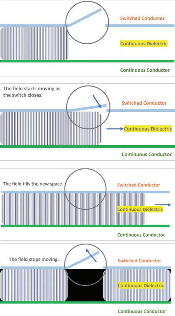
Put simply, we are all just plumbers
using leaky water pipes that happen to reside on a PCB. We design three-dimensional spaces for managing EM field movement (Figure 3).
Now consider power supplies. In a good design, energy is available whenever there is a demand, in the correct location, and connected with the appropriate plumbing. The impedance of the transmission line, not the resistance of the copper, is critical here. Adding heavier copper or more power vias is not the answer for higher current requirements. Matching the impedance to the demand is the key. Remember, the energy travels in the space. The solutions include wider power conductors, thinner dielectrics, or (my favorite) parallel dielectrics. You cannot get five gallons of water a minute through a one-gallon-a-minute hose by making it out of steel. The same goes for electromagnetic energy.
New problem: Moving this energy from storage to a load takes time. Wave velocity v for traces on a circuit board v = c/√ , where c is the velocity of light and is the relative dielectric constant: v = 150 mm /nsec or 6 in/ nsec. Electrons “drift” at the rate of 10-4 m/ sec. They have mass, so they cannot approach the speed of light — more evidence that the fields, not the electrons, are doing the work. All energy is moved by wave action. When a switch closes, a voltage drop sends a wave to get more energy. Each reflected wave can carry a limited amount of energy.
The job of the PCB designer is to match
5 MHz HMOS
the energy required for each type of switching event. As the geometry of the ICs we use continues to shrink, so does the area of effective power delivery. Well-defined power delivery transmission lines and small geometry, lowimpedance field storage devices are essential.
Switching Frequency vs. Power Source
4.92 feet
Rise time equivalent, 100 nanoseconds
Rise time distance, 100 feet
50 MHz (TTL Logic) UDR HCMOS
Rise time equivalent, 10 nanseconds
Rise time distance, 10 feet
500 MHz (BiCMOS Logic) IDR HCMOS
Rise time equivalent, 1 nanosecond
Rise time distance, 1 foot
5 GHz (GaAs Logic) 65 nm HCMOS
Rise time equivalent, 100 picoseconds
50 GHz 32 nm HCMOS
Rise time equivalent, 10 picoseconds
Rise time distance, 0.12 inches
Somewhere in the room
0.492 feet (5.9 inches)
Somewhere on the board, should be routed as co-planar pairs
0.0492 feet (0.59 inches)
Width of your finger, time to look at small geometry capacitors and power islands
0.00492 feet (0.059 in. or 1498.6 μm)
In the package
0.000492 feet (0.0059 in. or 149.86 μm)
On the die
29 DESIGN WORLD — EE NETWORK 2 • 2023 eeworldonline.com | designworldonline.com
Figure 2. Ralph Morrison’s rules of triplets
Wavelength
Frequency 1/20
Figure 4.
Figure 3. How energy really propagates in a circuit board.
PCB DESIGN
Ultra Precision High Reliability Resistors - RS73

• Excellent long-term stability with ΔR of ±0.2% & ±0.5% in reliability test
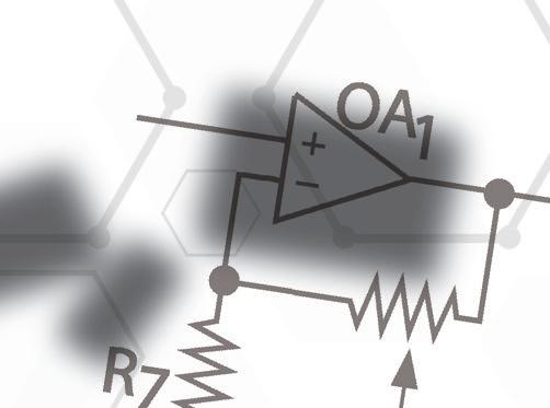
• Tolerance: ±0.1% ~ ±1%
• Resistance range: 10 ~ 10MΩ
Thin Film Resistor for Automotive - RN73H

• Improved moisture resistance by special protective coating

• High precision tolerances ±0.05% ~ ± 1%
• High performance TCR ±5 ~ ±100ppm/°C
Concept Reality to
Bring Your Designs to Life with Our Passive Components


Energy storage component geometry and placement requirements are determined by the device’s switching speed, not the clock frequency. The faster the switch, the more critical the geometry and placement. Do not expect behaviors from energy storage devices that are not possible due to their physical position or composition.
Critical factors include the distance from the switch, capacitor package size, and technology. The frequency at which capacitors can respond to energy requirements is determined by their physical geometry and the connecting transmission line, not by their value. Smaller capacitor packages respond faster because their terminals are closer together and provide more energy per wave cycle. Devices closer to the switch respond faster because it takes less time to request and deliver energy (Figure 4).
Oh, and by the way, energy delivery from power supplies is a one-way path! Current does not flow in a loop; it flows from the power source to the load. Each node in the power supply should be considered a discrete domain, with field energy traveling downstream from the power source to the switching device.
The key points to remember are:
• Electromagnetic fields travel in the space between the conductors, not in the conductors.

• Transistor switching speed determines the operation frequency, not the clock rate.
• Switching speed determines the power supply requirements, not just the dc current specification.
• Signal and power connections must be one dielectric from ground for their entire length (including layer transitions).
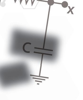
It’s All About the Space!
Surge Precision Resistors - SG73S

• ESD withstanding; down to ±0.5% tolerance
• Suitable for high peak voltages with short duration
• Resistance range: 1 ~ 10MΩ

Precision Thick Film Resistors RK73G
• High precision resistor with T.C.R. ±50ppm/°C
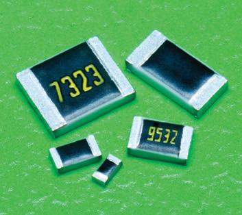
• Resistance range: 10 ~ 1MΩ
• Tolerance: ±0.25%, ±0.5%, ±1%

Anti-Sulfur Resistors - RT
• Broad family of resistors with excellent anti-sulfur characteristics


• Passes ASTM-809 anti-sulfuration testing


• Excellent heat resistance and environmental resistance
References
NXP Semiconductors, www.nxp.com
Ralph Morrison high-frequency design class, www.ralphmorrison.com
“A novel approach to power distribution: Building a solid foundation,” notes, https:// community.nxp.com/pwmxy87654/attachments/ pwmxy87654/connects/197/1/AMFAUT-T3882%20A%20Novel%20Approach%20 to%20Power%20Distribution_rev.pdf


POWER ELECTRONICS HANDBOOK
make your
To
design a reality, check
out our products!
www.KOASpeer.com
CommunicationAd_DW8_22.qxp 6/30/22 12:54 PM Page 1 30 DESIGN WORLD — EE NETWORK
2023 Webinar Series
Today’s electronic engineers are challenged by multiple factors. Research over the years has illustrated common trends that you, as engineers, deal with including keeping your skills up-to-date, shrinking time-to-market windows, fewer engineers and smaller design teams for large projects and evolving technological trends. The bottom line is that you must continually update your engineering knowledge base to be successful in your work.

Throughout 2023, we are presenting a series of online educational days where you can learn how to address specific design challenges, learn about new techniques, or just brush up your engineering skills. We are offering eight different Training Days. Each day will focus on helping you address a specific design challenge or problem. These are not company sales pitches! The focus is on helping you with your work.
MARCH 8, 2023
THERMAL MANAGEMENT
APRIL 12TH DESIGNING FOR SUSTAINABILITY
MAY 3RD EMI/RFI/EMC
AUGUST 9TH BATTERY MANAGEMENT
SEPTEMBER 13TH
MOTOR DRIVES DESIGN
OCTOBER 11TH IOT DESIGN / WIRELESS

NOVEMBER 8TH
For more information and to register for these webinars, go to:
EETRAININGDAYS.COM
ELECTRIC VEHICLE DESIGN
DECEMBER 6TH 5G / RF DESIGN
The case for AEC-Q semiconductors
in non-automotive uses
Specifying parts
in AEC-Q-certified
Kevin Parmenter,
Taiwan
Semiconductor USA
Electronic
components used in vehicles must have an AEC-Q100 qualification; this qualification means the device has passed specific stress tests and guarantees a certain level of quality and reliability. Of course, reliability is increasingly important in a variety of uses in those vehicles. So, it makes sense that parts manufactured to meet automotive quality and reliabilty standards would be used in other applications.
For example, emergency and medical systems leave no room for failure. One other advantage of AEC-Q parts: Automotive designs usually require an assured source of supply (not discontinuing components) contractually for 10 years or more. This assurance of supply can come in handy for other designs having life spans approaching those of vehicles.
High-reliability markets
It may be useful to review some of the details entailed in AEC qualification tests and what they demand on the part of component manufacturers. Devised by the Automotive Electronics Council, AEC-Q100 is basically a stress test qualification for packaged integrated circuits; it defines four temperature ranges that all start at -40°C and span progressively wider ranges with the highest at 150°C. There are similar standards for passive components (AEC-Q200), discrete semiconductors (AEC-Q101), discrete optoelectronic semiconductors (AEC-Q102), and multi-chip modules (AEC-Q104). Other than radiation testing, automotive qualification is equal to or more stringent than military requirements.
All these standards spell out numerous reliability tests. The entire list of tests is quite long, but the major categories
cover accelerated environment stress tests, accelerated lifetime simulation tests, packaging/assembly, die fabrication checks, electrical verification, defect screening, and package integrity.
Specific tests in the above categories include high-temperature storage, powered temperature cycling, and highly accelerated stress tests; checks of wire bond shear and pull, solder ball shear, and lead integrity; die checks for electromigration, stress migration, and time-dependent dielectric breakdown; and, of course, electrical tests. These can include fault grading, ESD and EMC checks, soft error rate and latch-up stress checks, and many others.
The AEC demands that these tests take place on random production parts, not on prototypes or hand-selected samples. Manufacturers must pull samples from three unique lots with a sample size of 77 per lot. Accelerated tests must run for 1,000 hours, and the manufacturing process must demonstrate repeatability; manufacturing parameters must have a CPK — a measure of the process spread and location — of at least 1.67. Specifically,
CPK=the distance from the mean parameter value to the nearest spec limit, divided by the distance from the mean parameter value to the process edge.
It is also interesting to contrast expectations for parts in ordinary consumer devices with those in vehicles. Where AEC-Q100 spells out a -40 to 150°C maximum ambient range, consumer goods typically get designed for only 0 to 85°C. Parts destined for consumer goods can have failure rates of 300 ppm and still be considered acceptable; in automotive uses, the acceptable failure rate is zero. Finally, new chips for consumer uses may only be produced for a few years; chips for new car models must still be in stock 20 years later.
Expectations for more robust electronic systems increasingly affect markets where products must operate in harsh environments. In many cases, product manufacturers have extended their warranty periods from three to five to seven, to now 10 years. In even the best-case scenarios, product failure can bring returns or repairs that nullify any sales profit
A search for a diode qualified for AEC-Q results in the 1SMA4741H, as shown. Search for part “1SMA4741” (no “H”) for non-automotive applications. The parts are identical –except that the “H” device comes with supporting AEC-Q paperwork.
32 DESIGN WORLD — EE NETWORK 2 • 2023 eeworldonline.com | designworldonline.com
built
fabs is an inexpensive way of creating exceptionally reliable, long-lasting designs.
POWER ELECTRONICS HANDBOOK
margins. In the worst cases, unsafe products can put customers at risk.
Industrial lighting is one such market. Service calls can be expensive, when it takes a union worker and a bucket truck to replace a fixture on a light pole or stadium catwalk. Many outdoor lighting devices see long periods of cold-soaking and hot sunlight, like those placed in potted modules. Yet they are expected to work flawlessly and last for many years.
Likewise, consider the HVAC and appliance market. As with industrial lighting, these systems must operate in extreme conditions. If HVAC systems fail during heat waves or freezing weather, the consequences can lead to safety issues and property damage (freezing water lines, elderly shut-ins put at risk and such).
The merchant power supply market is another area that requires reliability. These systems are used in a number of mission-critical medical applications. They also power public safety communications systems for fire, police, and EMS must remain operational.
The computing and networking markets also depend on servers, networking switches, and routers that are reliable. In these markets, profit margins are thin and expectations for uptime are high. More crucially, many industrial computing and industrial process control systems can create unsafe conditions on a wide scale if they fail. Again, these systems must continue to operate in electrically and environmentally challenging situations. Medical, avionics, broadcast electronics, plus a plethora of other applications must always remain operational.
Automotive-grade reliability for max advantage
Ten-year assured supply contracts are normal for
automotive suppliers. This situation has created a demand for semiconductor components with longer life cycles. The automotive industry already uses semiconductors in high volumes, and the electrification of transportation and advent of autonomous driving could make automotive the largest electronics market to ever exist. For this reason, suppliers often qualify entire families of parts to meet the automotive-grade standard, even if they do not label them as such.
Additionally, automotive suppliers see more price pressure than OEMs in many other areas. Semiconductor volumes in the medical industry, for example, are too low to impact supplier pricing. But medical instruments have long life cycles and need an assured source of supply. Ditto for numerous other electronics markets.
The factors at work in the automotive industry lead to this advice: when looking for a part for industrial lighting, safety, or similar applications, consider selecting an “automotive” device of the same type. In most cases, the top device suppliers do not classify parts families as “military,” “commercial,” or “automotive” by running multiple processes. Rather, they find it less expensive to run a single, zero-defects AEC-Q line to meet economies of scale. So, parts may be automotive qualified though they are not labeled as such.
A search for an AEC-Q qualified “diode” on Taiwan Semiconductor’s website will result in the 1SMA4741H device as one option. But note: The part number 1SMA4741 (no “H” in the part number) is identical. The only difference is paperwork. The “H” device is labeled as an “AEC-Q” part, which means it comes with paperwork showing it meets this qualification.
Both diodes were run on
the same factory control line and provide the same reliability. In other words, a designer with a non-automotive application can select the 1SMA4741 part and receive an AEC-Q audited part at no extra cost.
Designers selecting parts for non-automotive applications can ask suppliers like TSC to provide downloadable reports, including Mean Time to Fail-Failure in Time (MTBF-FIT), AEC-Q Standard Reliability Qualification reports and Production Part Approval Process reports (PPAPs). These reports prove the part meets AEC-Q standards in accordance with qualification processes and that the SPC controls and audits are set up for a zero-defects result. These reports further ensure that not only will the device meet the AEC-Q testing and qualification requirements, but also that production processes align with the requirements of the automotive industry from a quality, changecontrol, and lifecycle perspective.
Questions for suppliers
When specing an automotivegrade device for a non-automotive application, it’s helpful to ask a few basic questions:
1. Can the part be used for automotive as well as commercial applications and, if so, what are the differences in qualification and production between the two?
2. Does the supplier have MTBFFIT, AEC-Q Reliability and PPAP reports for the devices on their website, or can you obtain copies on request?
3. Can you see an AEC-Q qualification test report on the parts you are considering? (Often qualification is grouped by device family. For example, a specific 5-V Zener part number will be shown on the report alongside every part in its Zener family, ranging from
the lowest and highest voltages, i.e., a family qualification.)
4. Does the supplier have a “zero defects” approach, and can they pass an automotive audit? What is the supplier’s AQL level presently – it should be in the single digit parts per billion region.
5. Does the supplier sell to other top organizations that audit them on a regular basis to keep their qualifications current? Hint — so you do not have to.
6. Are the supplier’s certifications assigned numbers, proving that they are not counterfeit certifications? Some organizations “borrow” certifications from other websites and simply use adobe editor and modify them and use them as their own.
7. Finally, Is a contact available in your region or country? Some lesser organizations have no personnel in your time zone to talk to or often do not reply to attempts at communications. Field applications engineers and field quality managers in your region are a great place to start asking these questions.
In a nutshell, design engineers can benefit from using a component supplier that lets them select a part identical to one labeled as AEC-Q qualified. There are no downsides to designing a better quality, more reliable system at no extra cost. References
33 DESIGN WORLD — EE NETWORK 2 • 2023 eeworldonline.com | designworldonline.com
Semiconductor, www.taiwansemi.com AEQ SEMICONDUCTORS
Taiwan
Enabling a do-it-yourself hot-swap
circuit design using a hybrid architecture
Implementing a hybrid hot-swap circuit can make your life easier by eliminating a complex design process while ensuring robust protection, reduced solution size, and cost.
Durga Praveen G and Rakesh Panguloori, Texas Instruments
Thereis unprecedented demand for highly available and redundant systems to offer the best user experience. For example, in communications, banking, and industrial automated systems, any system downtime could potentially lead to lost customers.
The implementation of a hotswap circuit at the input of these systems protects against system faults and avoids system resets during power-supply disturbances. A hot-swap circuit comprises a hot-swap controller along an external metal-oxidesemiconductor fi eld-effect transistor (MOSFET) and sense resistor in the power path, as shown in Figure 1. As the power level of the module increases, the circuit requires more MOSFETs in parallel for lower path resistance and better thermal management.
A hot-swap controller generally has the option to program the current limit threshold (ILIM), power limit threshold (PLIM), and timer duration. During fault scenarios, the hot-swap controller regulates the MOSFET’s gate, forcing the MOSFET to operate in the saturation region so as to limit the current flowing in the power path, or power dissipation in the FET to their respective thresholds. If the fault condition persists, the MOSFET turns off after the timer expires; therefore, the MOSFET
used in the design must have safe operating area (SOA) limits high enough to withstand power loss during the timer period. For a more detailed understanding of MOSFET stress in different fault scenarios, see the Texas Instruments application report, “Robust Hot Swap Design.”
Challenges in traditional hot-swap designs
The traditional hot-swap circuit design process is complicated, involving multiple parameters and complex calculations. Selecting a MOSFET with an appropriate SOA that can withstand power stress in various fault conditions is one of the most important steps in a hot-swap design implementation. Designers also need to consider system-level specifications such as the maximum input voltage (VIN(MAX)), maximum load current (ILOAD(MAX)), total output capacitance (COUT), duration of transient load, and the maximum ambient temperature (TAMB(MAX)), along with FET parameters such as SOA, the drain-to-source onresistance (RDS(ON)), and the thermal resistance (R JA).
At the start of the design
process, you will not know which FET is right for your application. As you can see in Figure 2, the designer picks a FET based on VIN(MAX) and ILOAD(MAX) and goes through a series of complex design steps to find out whether the selected FET has an
SOA strong enough to meet the application requirements.
Here are the steps involved in the design flow:
1. Calculate the number of MOSFETs required in parallel based on ILOAD(MAX), TAMB(MAX), FET RDS(ON), and R JA.
34 DESIGN WORLD — EE NETWORK 2 • 2023 eeworldonline.com | designworldonline.com
Figure 1: Hot-swap circuit configuration
POWER ELECTRONICS HANDBOOK
Figure 2: Traditional hot-swap circuit design flow chart.
2. Calculate the time required for starting up into output capacitance. Designs with a large COUT require a transient voltage (dv/dt) control circuit with a capacitor (Cdv/dt) from gate to ground in order to limit the inrush current. Your startup time calculations should consider VIN(MAX), COUT, PLIM, and Cdv/dt.
3. Select a timer duration greater than the startup time and load transient duration.
4. Calculate the energy dissipated in the FET based on VIN(MAX), PLIM and the timer in different conditions, especially startup into an output short-circuit fault. To simplify the analysis, assume that the calculated energy is a square pulse with time (for example, tx) and that the power is the peak power dissipated (PFET) during a fault condition.
5. Estimate the amount of power stress that the MOSFET can handle for tx duration, as the FET data sheet may not provide the power-handling capability for the exact tx. This step involves the proper extrapolation of data in the SOA graphs approximating that the FET power handling vs. time follows a line on the log-log plot.
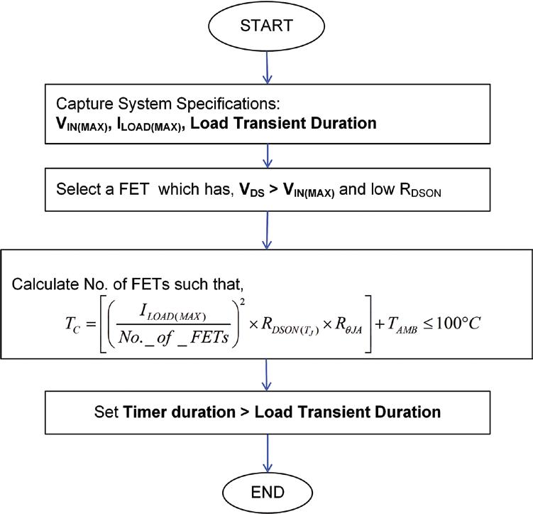
6. Derate the FET’s power-handling capacity for the maximum FET junction temperature based on ILOAD(MAX), TAMB(MAX), FET RDS(ON), and R JA.
7. Compare the power dissipated (PFET) in the FET during fault conditions to the derated power-handling capacity of the FET, checking whether there is at least a 20% SOA margin.
8. If the margin is less than 20%, restart the design process after improving at least one of these parameters:

• Selecting a FET with a lower RDS(ON).
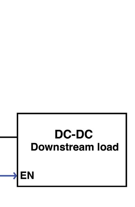
• Increasing the number of FETs in parallel.
• Reducing R JA by improving the layout.
• Selecting a FET with a stronger SOA.
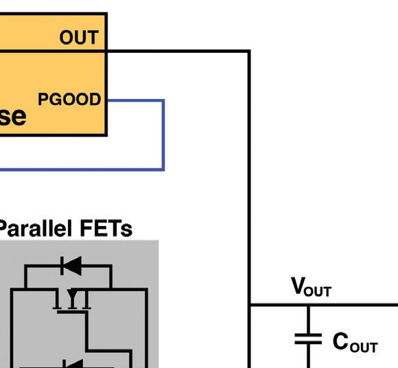
Every parameter change requires that the designer rerun the entire design flow to confirm whether the SOA margin is satisfactory. The entire design process is highly iterative and cumbersome until the designer finds a suitable FET. Texas instruments has design calculators for hot-swap controllers that can help when designing and reviewing the SOA margin for designs; however, engineers inexperienced in hot-swap circuit design may still find it difficult to select the most suitable FET.
Simplifying hot-swap design using a hybrid hot-swap circuit
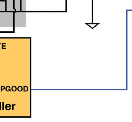
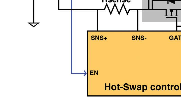
A hybrid hot-swap circuit consists of an eFuse connected in parallel with a traditional hot-swap circuit, as shown in Figure 3. An eFuse is a hotswap controller and MOSFET integrated into a single package, along with additional features such as thermal protection which protects the FET during power stress and ensures its operation within SOA limits. The power-good signal of the eFuse connects to the enable pin of the hot-swap controller, and the power-good signal of the hot-swap controller connects to the enable pin of the downstream load. These connections ensure that:
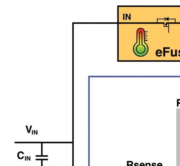
• The hot-swap FETs turn on only after the eFuse charges the large output capacitor close to the input voltage. The FETs start up with almost zero voltage across them, eliminating power stress during startup.
• The downstream load is enabled only after the hot-swap FETs are fully enhanced; the FETs can offer a low impedance path (compared to the eFuse) and share the majority of the load current.
• The eFuse endures power stress during all fault conditions, and the hot-swap FETs are not subjected to stress in any condition.
eFuses have an integrated overtemperature protection function that protects the internal FET by turning it off when the junction temperature reaches a certain threshold. eFuse devices such as the TPS1663 from Texas Instruments also have a thermal regulation loop that maximizes its internal FET power-handling capability during startup into capacitive loads and other fault conditions. Using this protection feature, the hybrid hotswap circuit is designed so that the eFuse is subjected to all stressful events. The hot-swap FETs are off during these conditions, thereby eliminating the most critical challenge in a traditional hot-swap design – the FET SOA. Using a hybrid hot-swap circuit and a FET with the lowest RDS(ON), eliminates the FET SOA, dramatically simplifying the design procedure. The design flow chart for the hybrid hot-swap circuit is shown in Figure 4. For highcurrent applications, you can simply calculate
35 DESIGN WORLD — EE NETWORK 2 • 2023 eeworldonline.com | designworldonline.com
Figure 3: Hybrid hot-swap circuit block diagram.
Figure 4: Hybrid hot-swap circuit design flow chart.
HOT-SWAP CIRCUIT DESIGN
the number of parallel FETs based on ILOAD(MAX), TAMB(MAX), FET RDS(ON), and RθJA. Choosing a lower RDS(ON) FET can reduce the number of FETs required in parallel, saving board space and reducing solution cost. Since the eFuse manages startup, you can set the timer duration solely based on the load transient duration.
Hybrid hot-swap circuit test results
The advantages of a hybrid hot-swap circuit over a traditional hotswap circuit become more significant when you realize that the power rating of the design increases. To easily understand these advantages, consider two test conditions: startup into a capacitive load and startup into an output short-circuit fault.
Figure 5 shows the waveform capture of a traditional hot-swap circuit during dv/dt startup into output capacitance. The math function signal in the waveform shows the power loss in the FET during startup. For higher output capacitance values, the power loss in the FET exists for longer durations, making it challenging for the FET to operate within its SOA. Similarly, Figure 6 shows startup into an output short-circuit fault waveform for a traditional hot-swap circuit. You can see that the FETs are stressed for the timer duration before the controller turns the FETs off, proving that FET SOA is a critical design parameter in a traditional hot-swap circuit, as the FET is stressed in different conditions.
Figures 7 and 8 show the waveform captured for the same test conditions with a hybrid hot-swap solution. Because the hot-swap controller is only enabled once the eFuse ramps the output voltage up to the input voltage, there is no current flow through the hot-swap FETs, and thus no power loss in them. The eFuse with integrated thermal protection handles stressful events and keeps the hot-swap FETs completely free from SOA limits, thereby simplifying circuit design procedures.
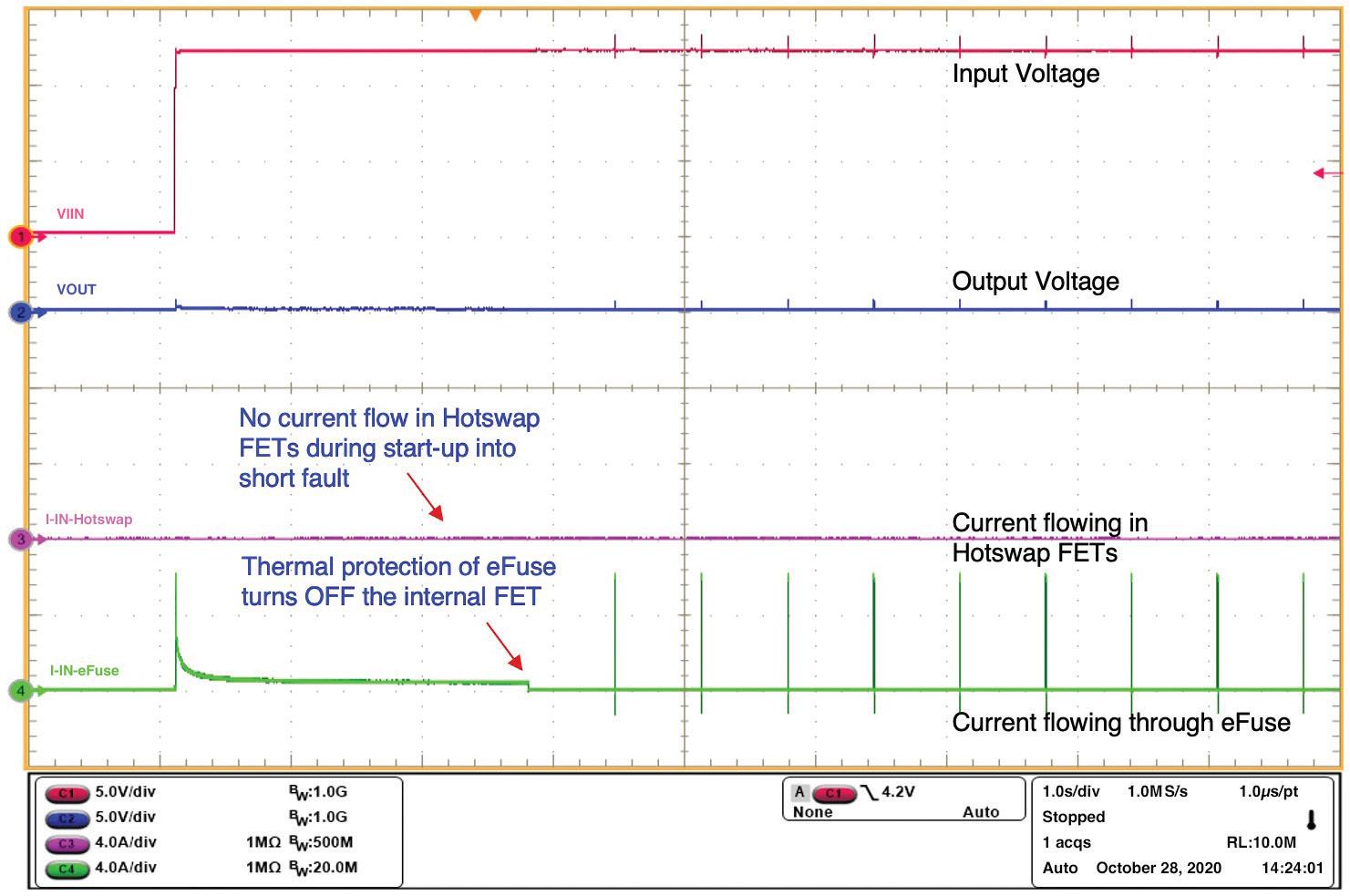
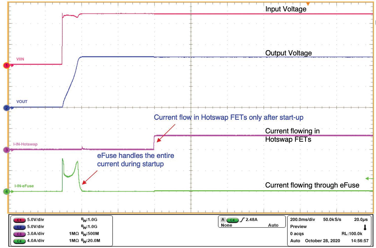
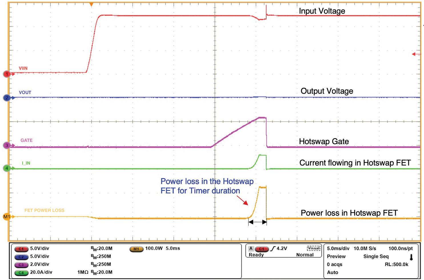
Designing an input hot-swap protection circuit is no longer a headache. Implementing a hybrid hot-swap circuit can make life easier by eliminating a complex design process while ensuring robust protection, reduced solution size, and cost. For a more detailed description of circuit functionality, advantages, design calculations, and test results of a hybrid hot-swap circuit, see the Texas Instruments Analog Design Journal article, “Protect Against High-Current Faults Using Hybrid Hot-Swap Architecture.”
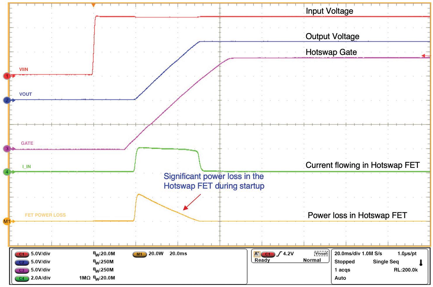
36 DESIGN WORLD — EE NETWORK 2 • 2023 eeworldonline.com | designworldonline.com POWER ELECTRONICS HANDBOOK
Figure 5: Traditional hot-swap circuit dv/dt startup into a 5-mF output capacitance.
Figure 6: Traditional hot-swap circuit startup into an output short-circuit fault.
Figure 7: Hybrid hot-swap circuit startup into a 30-mF output capacitance
Figure 8: Hybrid hot-swap circuit startup into an output short-circuit fault.
Find the Right Part Faster
Designed by Engineers for Engineers, our DC-DC Optimizer helps you find the optimal power inductors for your converter designs quickly and easily, reducing your design cycle time.
Coilcraft’s MAGPro suite of online inductor analysis tools are designed to enable inductor selection and circuit optimization based on sound engineering principles and measured data.

The DC-DC Optimizer starts with your power converter parameters, calculates the needed inductor specifications, identifies off-the-shelf part numbers, and provides
side-by-side performance analysis.
The tool identifies optimal inductors for buck, boost, and buck-boost converters. With just a few clicks you can go from VIN/VOUT converter requirements to inductor selection complete with losses and saturation analysis, all based on verified inductor data.


Reduce your design cycle time with confidence at www.coilcraft.com/tools.

WWW.COILCRAFT.COM ®
MAG Pro MagPro TM TM
MAGProTM
Bidirectional power supplies support new UPS requirements
We recently had a shortterm power failure in the neighborhood due to a storm and a downed tree. As the outage lasted only about eight hours, it was a minor inconvenience in the bigger picture of things but a major reminder of how much we depend on electrical power at home as a convenience and necessity.
Not surprisingly, the informal “standing in the street” discussion turned to the desirability of a residential uninterruptible power system (UPS), which ranges from about $5,000 to $15,000 installed, depending on capacity and installation issues. These home UPS systems (yes, saying “systems” is redundant with the UPS acronym, but everyone does it) are usually powered by a generator fueled by piped natural gas, diesel fuel, or propane in an on-site tank. Some have a battery bank as well or even exclusively (supercapacitors are sometimes used instead, depending on the load characteristics and other factors).
The generator-powered UPS is often referred to generically as a Generac system. That vendor is the market leader in the US, with about 60% of the market, while Kohler is second. They are not the same as a lower-cost, small, portable backup generator you manually connect and start when power fails.
One of the neighbors
Off-line UPS block diagram
remarked that he doesn’t understand why these consumer generator-powered UPS systems have a switchover time of about 10 seconds until they restore power. Commercial systems with battery backup have either no switchover time or one on the order of 10 milliseconds, depending on topology. After all, the UPS at the hospital usually assures no power interruption. His legitimate question was, “What’s the big deal with making it, so there is no interruption?” While asking that question is easy, the answer is not obvious. The technical reality is that a UPS designed to ensure no power interruption is a much more complicated, costly system with many more tradeoffs than one designed to allow for a brief interruption.
UPS: the two basic types
There are two broad classes of basic UPS systems, with several variations within each:
In the offline UPS approach, the load normally operates from the grid-provided AC line while the backup source (generator or batteries) is on standby if needed.
• Offline: also called a standby architecture, this is the mostcommon home/consumer approach. The load (house) normally runs directly from the utility AC line and grid. When the UPS controller senses a multi-second loss of power (more than a brief sag or brownout), it starts the generator (which is not needed for a batterysupported system). A static switch (transfer switch) disconnects the load (the house) from the AC line and connects it to the backup generator.
That generator’s AC output is rectified and converted to lineequivalent AC via an inverter (the battery, if present, obviously does not need this rectification stage).
Key to this operation are the “static
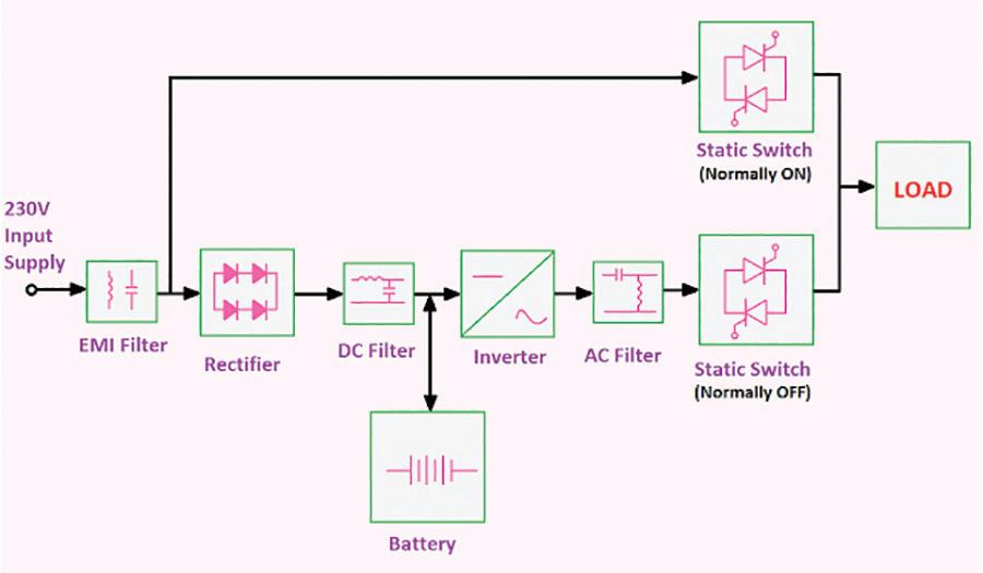
38 DESIGN WORLD — EE NETWORK 2 • 2023 eeworldonline.com | designworldonline
.com
Bidirectional power supplies dynamically direct power from multiple sources to different loads, some of which are also power sources at other times.
Bill Schweber
POWER ELECTRONICS HANDBOOK
BIDIRECTIONAL POWER SUPPLIES
On-line UPS block diagram
For the online UPS, the load operates from the UPS as the source, continuously recharged via the grid; the generator is activated while the system is still running on batteries.
the other as determined by the availability and load conditions. The load on each source may be independent of the other source’s load.
In contrast to a basic offline or online UPS, modern power subsystems and their applications must encompass a multiplicity of power sources and loads. Depending on the shifting power availability and needs, some of these will be a source at one time and load at another.
switches,” which provide a power-transfer function; when power fails, one static switch disconnects the AC line, and the other connects the backup generator (or battery) to the load.
There’s also a provision for charging the batteries from the AC line when power is on for a battery-equipped backup system. Most systems use an automatic sense/control for generator startup and switchover, although manual systems are available for about $500$1000 less, but what to do when the power fails if you are not home?
• Online: To offer continuous operation totally without any power gaps, the online approach (sometimes referred to as “double conversion online”) is used. The AC grid power continuously charges the batteries; even under normal conditions, the load operates from the batteries via the inverter. This sounds very simple and logical, but it brings some significant technical challenges, including inverter design, switchover, and battery sizing and management issues to maximize run time and battery life.
Some commercial systems use batteries only and do not have a generator, which trades one set of limits (battery runtime) for another (generator issues). Some home systems, such as the Tesla Powerwall or the Generac PWRCell, also use batteries exclusively, and they are recharged via the grid or solar panels. Still, there is significant added cost and complexity. Also, some locales have zoning regulations regarding having installed charged batteries above a certain capacity in residential areas (electric vehicles are a carve-out exception, of course).
In some ways, the best system combines battery and generator: the battery carries the load through short disruptions with little or no interruption, while the generator is used for longer outages. As always, it’s a complex set of tradeoffs among cost, complexity, and capability.
Of course, this is a highly simplified overview of the reality of UPS architectures, sub-architectures, and variations (some widely used, some proprietary). Nonetheless, it does indicate that the answer to the seemingly simple question of why most home UPS systems have a switchover interruption is neither simple nor obvious. One thing is clear: power comes from a primary and a backup source in these basic UPS systems and flows to the load. When the AC line is available, things are “quiet” in terms of power flow and shifts.
Role of bidirectional supplies in UPS
In recent years, there has been a dramatic increase in the need for bidirectional AC/DC and DC/DC power supplies, in addition to the unidirectional supply of a traditional UPS. That supply takes a source (such as the AC line or battery, or in some cases, a high-voltage DC line) and converts and regulates it to provide a DC-rail output for a load. In contrast, the bidirectional supply has multiple independent power sources. It can transfer energy from one to another as needed or available, as well as to the system’s primary load itself.
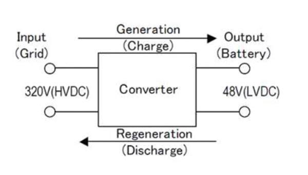
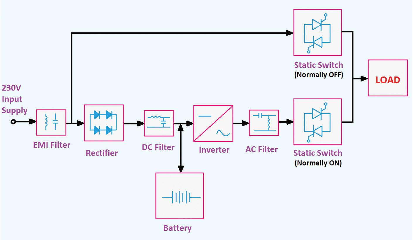
Bidirectionality with two power sources is not the same as simply having two independent power sources in parallel for higher capacity or in a redundancy arrangement where either can supply the system load. Instead, it involves continuous power flow management from one source to
The objective is to take power from where it is available at any given time (such as from high-voltage AC or DC lines or solar panels) and send it to a primary load. If excess power is available, it can also go to storage (a battery, in most cases) for later use. Still, it can also draw on the battery if the primary source is unavailable.
Note that the local power user (the local load) can be an individual residence, neighborhood, commercial office building, or even a medical/industrial setting. Some excess power may come via regeneration, such as from elevators or industrial motors.
While there are differences in the specifics of sources, loads, their magnitude, their
In one basic configuration, the bidirectional supply allows energy to flow from a high-voltage supply at the grid to a low-voltage battery and vice versa.
priorities, and the load’s dynamic range and criticality, they all have similar issues from a high-level perspective. Of course, there are differences – and these can be significant – due to power capacity and sizing of their various elements and functional criticality. In short: it can get complicated.
There’s another consideration when using a bidirectional converter. For line-operated systems, the previously captured and stored energy can supply additional power needed at the startup when large amounts of torque are required. This topology saves energy overall and allows for a smaller AC-line power
39 DESIGN WORLD — EE NETWORK 2 • 2023 eeworldonline.com | designworldonline.com
Cooling Fan Fuel Pump
Screens Heating
Bidirectional supplies are now used in automobiles to shift available energy between the 48-V battery used for heavier loads and the 12-V battery for lighter loads.
subsystem, as the peak demand on the line-side supply will be reduced.
A similar arrangement is used in battery-backup situations. The AC line powers the load and charges the batteries, which are also charged via solar panels. When AC power fails, the batteries power the load through the bidirectional converter and can still be charged by the panels. Thus, the system has power flowing to where it is needed from where it is available.
The use of bidirectional supplies is not limited to high-voltage/ high-current applications. Many of the latest cars, including those with traditional internal combustion engines (ICE), now use a dual-battery power system. These have a 12-V battery for lower-power loads, a 48-V battery pack for efficiency, and smaller conductors for higherpower loads).
In this dual-source/dual-rail topology, it is necessary to continually assess if each battery has sufficient capacity to support its loads and transfer power at any time from the battery which has adequate capacity to the one which may be lacking it. This is the case even though the ICE alternator will be charging both batteries but cannot do so quickly enough.
Conclusion
Today’s power components and the systems they support are expected to be compact, efficient, and reliable. At the same time, new functional demands are being placed on them to handle more types of sources and loads under a complex set of power-flow scenarios. Key to this challenge is the development of bidirectional power supply and powermanagement units.
References
Recom, “How to make a 10kW bidirectional AC/DC converter”
MEAN WELL, “Application of Bidirectional Switching Power Supply with Energy Recycle and AC Grid Function”
Vertiv Group Corp, “What Are the Different Types of UPS Systems?”
Unified Power, “Which UPS Topology is optimal for your environment?”
Schneider Electric, “The Different Types of UPS Systems”
EtechnoG, “Offline and Online UPS Block Diagram”
Cabling Installation and Maintenance, “A generator-friendly uninterruptible power supply”
This Old House, “BackupPower”
Elprocus, “Uninterruptible Power Supply Circuit Diagram and Working”
Green Tech Media, “Generac, the Backup Generator Giant, Launches Souped-Up Home Solar-Storage System”
40 DESIGN WORLD — EE NETWORK 2 • 2023 eeworldonline.com | designworldonline.com POWER ELECTRONICS HANDBOOK
Bidirectional Current Flow KL30 12 V KL31 KL31 KL41 KL40 48 V KL41 3P M / G Mechanical Coupling to ICE Passenger Safety Engine Management Driver Assistance Transmission Control Brake System Infotainment - - -
Air Conditioning Water Pump
Electric Heating EPS
Roll Stabilization Inverter - -DC / DC
THE POWER OF SIMPLICITY
Isolated Gate Drivers with No External Bias Power Supply
RELIABLE
Only 3 external components
SMALLER
50% solution size reduction
EASY TO USE
Isolation solution in single package
3 5
ISOLATED DC-DC BIAS SUPPLY ISOLATED GATE DRIVER

ALLEGRO AHV85110 SELF POWERED ISOLATED GATE DRIVER
DESIGNING AN ISOLATED GATE DRIVE CIRCUIT HAS NEVER BEEN AS EASY AND AS FAST


allegromicro.com/gate-drivers

Key considerations when integrating high voltage dc-dc converters into critical applications
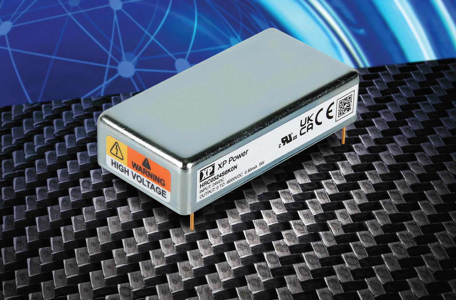 Hafiz
Hafiz
Overthe years, through observations in the field and conversations with design engineers, four challenges regularly present when integrating high voltage dc-dc power modules into critical, long-term applications. The most important criteria is to define the requirements of the power module correctly, then consider the converter’s accuracy under various conditions, the surrounding circuitry required, where it should be placed relative to the converter, and how to integrate the module into the final design.
Defining key parameters
When looking for a high-voltage power module, a critical starting point in the design-in process is to define its requirements accurately. Depending on the application, this covers all the significant
parameters of the module. Therefore, the first step is to understand the input and output conditions in the application. The input voltage and its accuracy define the module’s necessary line regulation and protection requirements. In most cases, the load and loading conditions are complex but, once known, help define the basic parameters of the module, such as voltage, current, and polarity. A typical photomultiplier tube, for instance, may require 1200 VDC at a few micro-Amps of current. Additionally, knowing what signals are available to control and monitor the module so that it operates correctly and safely enhances the end application.
There are also environmental conditions to consider. For example, designers must pay attention to elevated operating temperatures or moisture levels if the end application is in equipment destined for installation in the tropics. So too, are space constraints; generally, the focus on equipment, from handheld devices to
benchtop test & measurement instruments, is to make them as small as possible or pack more functionality in the same space.
Last but not least are the required agency approvals for the end equipment. A typical example is the UL/IEC/EN 61010 standard for analytical instruments. Selecting a pre-approved module to the relevant standards eases design-in saving time and money.
Assessing accuracy
Once the requirements of the power module have been defined correctly, its overall accuracy needs to be assessed. Accuracy can be affected by variations in the input voltage, loading conditions, operating temperature, and various other environmental factors. For example, consider the output voltage tolerance, which defines any variation from the specified voltage. There is also the set point accuracy of the module to consider, which confirms its ability to achieve the set point using the control voltage.
Again, line and load regulation specify the module’s ability to keep the output voltage within certain limits, regardless of the input or load variations. Ripple and noise can also impact the accuracy of the module. For certain power module applications, such as analytical instrumentation, output stability over time is essential to ensure repeatability. For example, this stability over time becomes critically important in mass spectrometry, where equipment can run for several hours. Here, the instrument must deliver the same results if the same sample goes through twice. Changes in ambient temperature can affect the output voltage as well. Usually, the module’s long-term drift and temperature coefficient are specified on the datasheet.
XP Power’s HRC05 power module delivers accurate high voltage with the specifications you need.
42 DESIGN WORLD — EE NETWORK 2 • 2023 eeworldonline.com | designworldonline.com
Knowing precise parameters up front goes a long way to ensuring your critical application meets performance expectations.
POWER
Khalid, Director of Product Marketing at XP Power
ELECTRONICS HANDBOOK
Surrounding circuitry
As opposed to low-voltage or digital circuit boards, designing a high-voltage circuit board requires particular attention to the surrounding componentry, especially on the secondary side of the module. Designers should keep a close eye on the creepage and clearance distances from low-voltage circuitry, to ensure there are no ground planes, silk screens, or plated holes in the high-voltage area.
If isolation is required, consider adding slots on the board. It is also good practice to avoid sharp edges on the pads on the circuit board and consider using a conformal coating or other insulating materials if required. When specifying components for high voltage applications, please note their voltage/power ratings and derating. Voltage/ temperature coefficients and the thermal performance of the components themselves also play a significant role when designing high-voltage circuitry.


Electrical module integration
There are various built-in features to look out for when selecting a high-voltage power module that aid handling and ease integration, simplifying and shortening design times. For example, many modules feature undervoltage and overvoltage protection circuitry to protect from glitches on the input line. There may also be circuitry that prevents the misprogramming of the control voltage, protecting the module from inadvertent damage.
On the secondary side, arc protection prevents damage to the module due to arching events in the applications. In addition, overcurrent and short circuit protection circuitry provides safety for the module and application in case of a fault condition, such as an overload or short circuit. Likewise, thermal shutdown protects the module if the temperature rises above its specified operating temperature range. There are various thermal shutdown mechanisms; regardless, most power modules recover once the over-temperature condition is removed.
Controlling and monitoring the module
The digital compatibility of the signals used to control and monitor the power module defines the circuitry required. For example, many power modules feature digital-toanalog compatible signals, making it easier
to control the high voltage. General lab equipment, such as digital multimeters and scope probes, are often limited to 1 KVDC, which makes measuring the high voltage of the power module a challenge. Power modules with digitally compatible monitor signals, however, negate the need for using an instrument altogether, making it much easier for the design engineer.
Mechanical module integration


On a practical level, there are many more things to consider when integrating a highvoltage power module into an application than a low-voltage module. In many cases, the input and output pins are solderable, but other connection types are also available. Also, knowing the number, position, and type of pins is important to ensure the safe routing of the PCB traces and compliance with the safety requirements, such as creepage and clearance. Knowing the physical size of the
module is also essential, both the footprint and height; its overall weight a key consideration as well, especially if the designer knows that the end application will likely encounter shock/vibration loads, however infrequent. Finally, if additional heatsinking is required on the module, this must be factored into any size/weight considerations and whether affi xing it is compatible with the production process.
Conclusion


Recognizing the need for a highly reliable, high-voltage dc-dc converter with precise output specifications is only the start of the design-in journey. XP Power can help you with technical support and product samples. For more information, please visit: www.xppower. com/high-voltage-dc-dc

MADE IN THE U.S.A. SHOCK & VIBRATION SOLUTIONS NEW! STANDARD PRODUCTS GUIDE NEW SITE OVER 600 PARTS 800.838.3906 sorbothane.com Sorbothane_DesignWorld_Ad_12-2022_r2.indd 1 12/19/22 9:13 AM 43 DESIGN WORLD — EE NETWORK
HIGH-VOLTAGE DC-DC CONVERTERS
DESIGN SPOTLIGHT


Custom Power Magnetics Solutions


With more than 80 years of experience, you can count on Triad as your custom power solution partner in factory and home automation, industrial equipment, power conversion, renewable energy, medical/ dental equipment and more.


• Power ratings from 0.010VA to 9 kVA, series or parallel configurations
• Fequency ratings from 20 Hz to 500 kHZ to meet all design needs
• Highly dependable eliminates noise and suppreses noise for EMI/RFI filtering
• Wide range of material types including micro wire winding, packages and configurations
We start by listening to your needs. The custom product engineers at our California Design Center have the latest CAD/CAE systems with rapid prototyping, electrical testing and production sampling to help you.

• Industrial, consumer and medical grade, 25 to 10,000 V-A, in series or parallel design
• Cores: iron, iron oxides, nickel, zinc, magnesium and grain oriented silicon steel

• Input 100 to 240 Vac; Output 4.5 to 24 Vdc, meet EISA 2007 efficiency standard

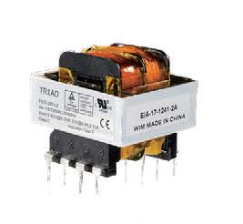

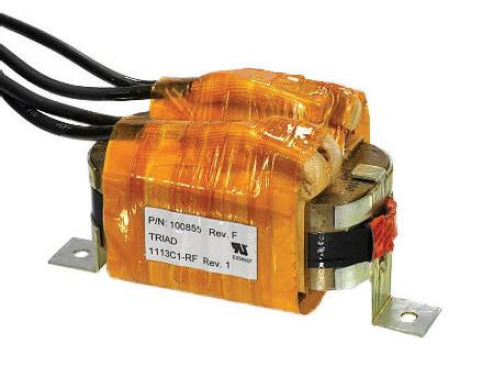
• Unique packaging, custom colors, UL/TUV approved, global modular designs
We guide you step-by-step, explaining options affecting performance, life, materials, safety and cost. We’ll help you optimize your design for highest performance at the lowest cost.
• Choose from all the standard lamination materials or Triad’s custom materials


• UL/TUV certified insulation systems from 130 to 200°C
Triad also offers dozens of standard power magnetics transformers and inductors that might meet your needs. They’re ready to go right off the shelf. Our goal is to provide the lowest-cost solution that meets your needs. Ask our expert design team for help today.
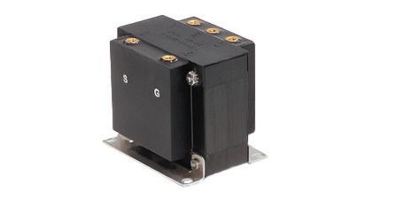
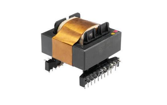
Our manufacturing plants are in multiple locations, including the Philippines and the US, which helps mitigate risk. Triad’s quality systems eliminate the need for inspection.

• Hi-frequency to large three phase, dc and ac types, chokes, reactors and more
• Select from a choice of materials magnet wire, Litz wire, copper foil and aluminum foil
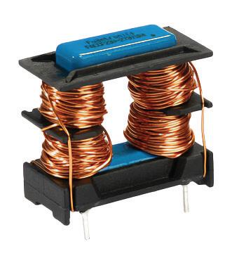
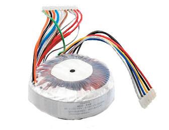
For info or to purchase, go to: www.TriadMagnetics.com Triad Design Help Desk 800-624-6384 MAGNETICS Custom Switch Mode
Toroidal Power Transformers
Wall Mount Power Supplies Custom Laminated Power
Ask About Standard Designs
Custom Current Sense Transformers
Transformers Custom
Custom
Transformers
Too!
Custom High Current Inductors FREE Triad Custom Design Guide
QUALITY S E R V ICE VALUE 80 YEARS Of EXCELLENCE 1943-2023
Selecting dc-dc converters
for railway applications
Historically,
the 110 V battery located in the main locomotive [EOL1] was the source of dc power for most electrical rail applications. This meant in order to provide light to the carriages, cables ran along the full train length.
Since the battery was also connected to switchgear, relays, and other heavy electrical loads like starter motors, the cable voltage was prone to dropouts and transient spikes, as well as electromagnetic and radio frequency interference (EMI/RFI). Though passengers remained largely oblivious to these effects, apart from experiencing occasional shifts in cabin lighting levels.
Modern trains are much more technically advanced than their predecessors. They now include many advanced safety features which use multiple low voltage sensors and actuators. Additionally, contemporary rail passengers have come to expect their travel experience to include comforts like air conditioning, wireless communication, and sophisticated infotainment features.
These new features require power at a range of voltages and power levels; dc-dc converters are used to convert the battery supply voltage to the proper levels for
electronic devices and must do so safely
and reliably under a wide range of operating conditions presented by rail applications. Ensuring safety and comfort would not be possible without the availability of multiple power supplies to provide constant dc voltage levels uncontaminated by external sources of electrical noise. In this article, we will review some of the specific requirements for using dcdc converters in rail applications.
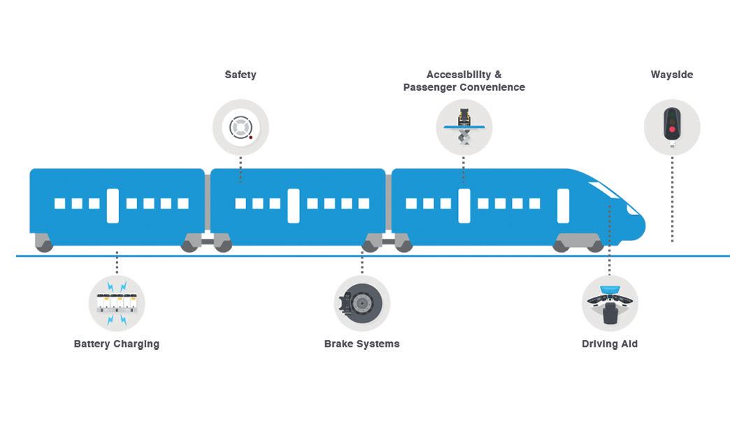
Railway power standards
A number of national safety standards have been developed to address the safety concerns of rail applications. These include the British RIA12, French NFF 01-510, and European EN 50155. The EN 50155 standard applies to electrical equipment supplied to the railway industry and has been adopted by most railway equipment manufacturers. It relates to battery-powered systems and low voltage power supplies that are directly (or indirectly) connected to the
contact system and cover control, adjustment, protection, and supply applications.
Dc-dc converters in power in-vehicle electronic equipment must adhere to EN 50155 in each of the following ways:
Input voltage range
The battery voltages most used in rail applications are 24 V, 48 V, 72 V, 96 V, and 100 V. The inevitable dips and surges caused by demand from multiple onboard systems mean these levels vary widely. EN 50155 specifies that these are allowed to range from 0.7 to 1.25 times their nominal value, with more significant transient variations of 0.6 to 1.4 nominal (for durations up to 100 ms) also being acceptable.
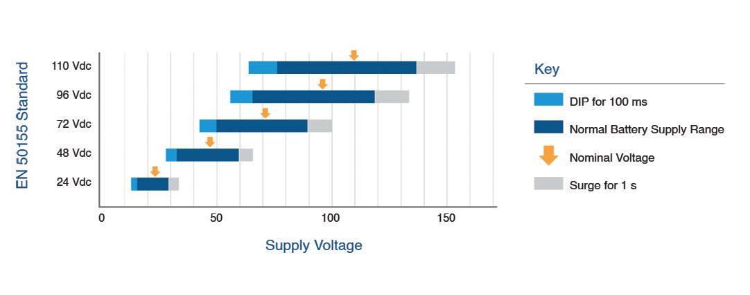
Electromagnetic compatibility
Dc-dc converters are notorious emitters of electromagnetic interference, as the interface to the power source is also subject to power surges and other disturbances. Like many applications there are specific emissions and immunity requirements for power converters used in rolling stock applications — they are specified EN 50121-3-2.
The Electromagnetic Compatibility (EMC) requirement for electrical equipment is defined by how it interfaces with the external environment. These interfaces are known as ports. Different ports have different EMC requirements. For battery ports, there are no conducted emissions limits in the frequency of 9 kHz~150 kHz. The same EMC requirements apply to batteryreferenced, signal and communication, process measurement, and control ports.
45 DESIGN WORLD — EE NETWORK
2 • 2023 eeworldonline.com | designworldonline.com
Bel Fuse Inc.
The wide range of voltages and power levels required in modern trains puts a special focus on the role of the dc-dc converter.
Examples of different systems requiring power throughout a train.
CONVERTERS FOR RAILWAY APPLICATIONS
EN 50155 Supply voltage ranges
Mechanical shock and vibration
Electronic equipment must be able to withstand the levels of shock and vibration experienced by a train in regular service, without degradation in performance. These levels can be defined by the train supplier. Otherwise, they must meet the requirements of EN 61373 category 1, Class B (Table 1).
Temperature and humidity
Electronic equipment must be designed to operate to its full specification based on a range of different temperature classes (Table 2). The environmental conditions of rail applications can vary widely and change rapidly.
Passenger and driver compartments are covered by classes OT1 and OT2 (with a standard reference temperature of +25°C). Classes OT3 and OT4 cover equipment in technical cabinets (with a standard reference temperature of +45°C). OT3 is the default class.
In addition to temperature and humidity, salt mist and pollution can cause concern by negatively affecting converter performance if not designed for it.
Isolation voltage
A key feature of dc-dc converters is the dc isolation provided by the transformer. Isolation isn’t perfect, however, and dc-dc datasheets will specify a test voltage rating. Depending on the battery voltage,
the dc-dc will have to be rated for a certain isolation voltage. These specifications ensure that conductors within the power supplies have sufficient electrical insulation and physical spacing so that leakage currents and electrical arcing are not issues. This test consists of two parts:
1. An insulation resistance measurement that is performed at 500 Vdc — the minimum level of insulation resistance required is 20 Megaohms.
2. The second part is a voltage withstand test (Table 3). Voltage levels are increased slowly (typically over 10-second intervals) up to the maximum value. The voltage is maintained for ten seconds or one minute, depending on the purpose of the test.
Fire and smoke
Fire safety is another critical aspect when engineering railway transportation applications. Power solutions must support the safety of everyone involved, both in terms of performance and flammability, smoke generation, and the potential for toxic chemicals to be released. The flammability rating for such applications should be UL 94V-0, and the standard related to this particular environmental challenge being EN 45545.
Other dc-dc selection considerations
Form Factor
product using the standard DIN 41612 H15 connector and is available at many power levels, and with many options. Both chassis-mounted and cassette style products will typically have “bus” outputs of 12, 24 or 48 V.
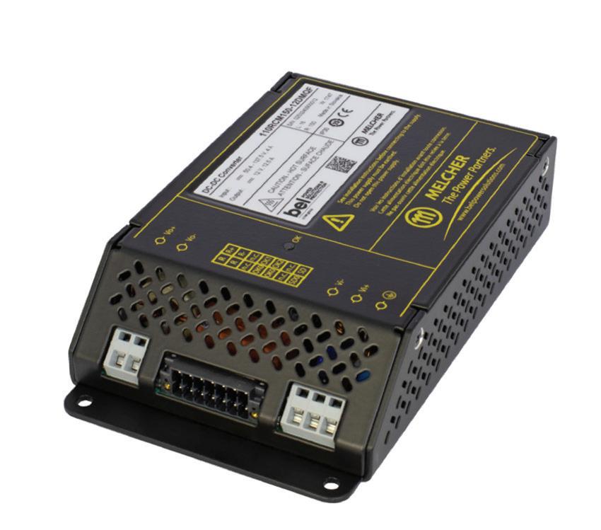
Hold-up time
Power converters designed for rail applications will often have options for extended hold-up time, which is the time that a dc-dc converter will have to maintain regulation after a loss of input power. “Holdup” or “ride through” can be quite challenging for low nominal input voltages and can require a large amount of external capacitance
Conclusion
Electronic devices used in rolling stock applications undergo a variety of electrical, environmental, and physical stresses during normal operation — Dc-dc converters are no exception, despite being a key component in many of the new features and devices found in modern trains.
To ensure safety and reliability, dc-dc converters must go through the rigorous testing prescribed by relevant safety standards. EN 50155 is perhaps the most common railway standard for electronic equipment, and many off the shelf dc-dc converters have been tested to it.
OT1
OT2 -40 to 55
OT3 -25 to 70
OT4 -40 to 70
OT5 -25 to 85
OT6 -40 to 85
DC-dc converters with various form factors are used in rolling stock, depending on the power level and application. Chassis-mounted parts are typical at higher power with appropriate ruggedization to meet the shock and vibration requirements with any open PCBs lacquered. Up to around 600 W, the Euro cassette style is very popular. This is a rack-mounting
if the dc-dc is not designed for it. For example, to hold up a 100 W supply at 80% efficiency for 10 ms for “Class [EOL2] 2” applications with an input range of 16-36 V around a 24 V nominal would need a capacitor on the input of about 8,000 µF rated at 40 V — about 2.5 cu-in or 40 cu-cm size. This is significant in both size and cost, and a major contributor to the overall reliability and lifetime calculations.
EN 50155 describes interruptions as being caused by input short circuits; so a series input diode is also necessary to isolate the hold-up capacitor, which causes an additional power loss and voltage drop, requiring the input range of the converter to be extended. Other solutions for hold-up might be to internally boost the input to a higher voltage so a smaller capacitor can be used for the same energy storage. But in any case, inrush current and charge rate into the capacitor must be controlled and may limit the repetition rate of allowable dropouts to 1 in 10 seconds or so.
However, with such a wide range of powered devices in rail applications, there’s not always an optimal off-the-shelf solution. For these cases, Bel Power offers extensive capabilities to modify and customize power supplies so designers can get the most out of their power supplies, no matter the application. Bel Power’s railroad power solutions answer the need for high power density and come in a variety of mounted solutions, meeting industry requirements and complying with the relevant railway standards for your design.
46 DESIGN WORLD — EE NETWORK 2 • 2023 eeworldonline.com | designworldonline.com
Vibration Category < 0.3kg 5-150Hz 5g Shock Long./Trans./Vert. axis 5g/3g/3g 30mS/30mS/30mS
Performance EN 50155
Class Operating Temperature Range (°C)
Table 1: Shock and vibration tests
-25 to 55
Vehicle Battery (V) Isolation Requirement VAC (50Hz)/DC 24 500/750 48 500/750 72-125 1000/1500 125-315 1500/2200 Table 3: Isolation and withstand tests specified in EN 50155
Table 2: EN 50155 operating temperature classes
RCM300 series 300 W chassis mount dc-dc converter for railway applications.


Infineon semiconductors are at the heart of renewable power generation. Enabling more while using less. www.infineon.com/green-energy
SALES
Jami Brownlee jbrownlee@wtwhmedia.com 224.760.1055
Jim Dempsey jdempsey@wtwhmedia.com 216.387.1916
Mike Francesconi mfrancesconi@wtwhmedia.com 630.488.9029
Courtney Nagle cseel@wtwhmedia.com 440.523.1685
Jim Powers jpowers@wtwhmedia.com 312.925.7793 @jpowers_media
LEADERSHIP TEAM
805.895.3609 @mmatheson
48 DESIGN WORLD — EE NETWORK 2 • 2023 eeworldonline.com | designworldonline.com AD INDEX POWER ELECTRONICS HANDBOOK • FEBRUARY 2023 Allegro MicroSystems ............................................ 41 AMETEK Programmable Power 19 APEC ..................................................................... 25 B&K Precision 2 Coilcraft 37 Digi-Key Electronics IFC Eaton Electronics 5 Infineon Technologies Americas ............................ 47 Keystone Electronics Corp 1 KOA Speer Electronics .......................................... 30 Kyocera AVX BC Pico Electronics ....................................................... 3 Quantic Electronics 11 Sager Electronics IBC Sorbothane 43 TDK Electronics, Inc. 7 Triad Magnetics ..................................................... 44 @ DESIGNW O R L D Publisher Mike Emich memich@wtwhmedia.com 508.446.1823 @wtwh_memich CEO Scott McCafferty smccafferty@wtwhmedia.com 310.279.3844 @SMMcCafferty EVP Marshall Matheson mmatheson@wtwhmedia.com
THERMAL SOLUTIONS


Sager Electronics offers standard and custom thermal products to meet any cooling requirement. From fans, blowers and impellers to heat sinks, thermal performance materials and more – no matter your needs, think Sager when you think thermal.


WITHOUT THE RIGHT THERMAL SOLUTION YOUR PROJECT COULD BE TOAST.
A SPECIALIZED GROUP WITHIN SAGER ELECTRONICS sager.com | THINK THERMAL
WITH KYOCERA AVX COMPONENTS

CIRCUIT PROTECTION

KYOCERA AVX offers State of the Art protection against damaging transient pulses, power surges, and temperature changes for many electronic circuits.


CAPACITORS
KYOCERA AVX offers an extensive portfolio of capacitors which covers most dielectric options available on the market today. These capacitors can be found in many industries including automotive, industrial, telecommunications, defense, and consumer electronics.

POWER/CHIP FILM

KYOCERA AVX produces a full range of film dielectric components – from low power SMD solutions for the commercial and automotive industry, to medium and high power film capacitors suited to all power electronic applications over a voltage range spanning 75V volts up to 100 kV.