5 minute read
Placing and matching a multilayer chip antenna


How to get the maximum performance from a multilayer chip antenna with respect to antenna placement on a PCB and effective impedance matching? Würth Elektronik’s Muhammad Ali Khalid and Richard Blakey explain.
Muhammad Ali Khalid Richard Blakey
Advertisement
The trend to miniaturize wireless communication devices has led to decreased PCB sizes and increased component densities. Although this shift has aided many areas of electronic design, it constrains RF front-end design. Due to the nature of antennas sending and receiving electromagnetic signals, they interact and are affected by the entire surrounding environment and are extremely sensitive to electromagnetic fields. This can be extremely problematic for RF engineers when integrating into a design an antenna that’s small, has good gain and efficiency in the frequency range of operation and is able to work as desired in different PCB environments.
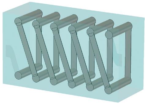
Multilayer chip antennas are an interesting choice for engineers who are restricted by cost and space requirements in wireless system design. Such antennas are formed from several layers of dielectric material, which are pressed and fired together into a monolithic structure. Each dielectric layer has patterned metallization on the surface that connects to other layers through vias. The inner conductors and vias form a radiating, multilayer meander structure, allowing the component to be smaller than a monopole antenna while achieving comparable performance. Electromagnetic fields are generated by the currents on the inner conductor.
PCB placement When incorporating an antenna into an electrical product, some of the most critical stages of product development are the PCB layout and the design of device enclosures. This is due to PCB component density continuously being increased to reduce the size of the device while not impairing the function of the design. Antennas can be extremely sensitive to power and ground planes when functioning as a λ/4 monopole antenna system. However, if the feedline and ground plane dimensions are carefully and intelligently taken into consideration when designing a chip antenna PCB, performance comparable to a λ/2 dipole antenna can be achieved.
The positioning of the multilayer chip antenna is critical to achieving optimum gain and performance. Not following the design rules can significantly reduce the gain. Generally, the closer a grounded conductive material is positioned to the antenna, the lower the performance will be.
The PCB corner is usually the most desirable location. This typically results in better
antenna gain as there’s only ground plane on two sides. When it’s not possible to place the antenna on the corner, it may go on the side of the PCB where it’s surrounded on three sides by ground plane, although the performance may be reduced.
In extreme cases, the antenna may be positioned over or between ground planes. However, it must be noted that having any metal plate or battery above or below the antenna will also result in significant performance degradation. In some cases, there’s no other alternative except to utilize the area above or below, so careful consideration must be taken during the design and prototype stages to ensure sufficient antenna gain performance.
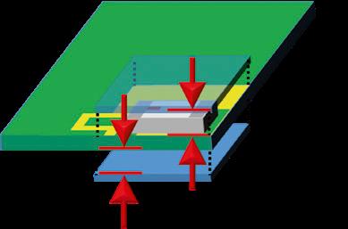
Special considerations should be taken into account when an antenna is placed in an enclosure. Completely encasing it in
Internal structure of the WE-MCA multilayer chip antenna
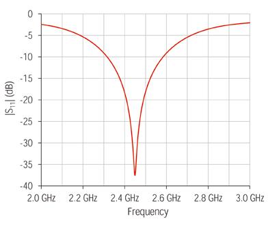
Simulated S-parameters of the WE-MCA multilayer chip antenna
metal is out of the question since the majority of the power from the antenna will be reflected back into the device. Housing made of non-conductive materials, such as plastic and glass, are much easier to incorporate into a design than conductive materials. Although the power isn’t reflected, the impedance and overall performance will be effected. Depending on the non-conductive material permittivity and proximity to the antenna, a significant frequency shift of up to hundreds of MHz can be expected. This needs correcting with appropriate impedance matching.
Impedance matching Usually when a chip antenna is designed, the electrical specifications are measured on a manufacturer’s test board, in free space. In reality, an antenna will be operated in an environment that results in an impedance transformation, regardless of whether it’s intended or not. The impedance mismatch will be different for every device.
Return loss is a good measure of how well an antenna is matched to its feed line. This measure quantifies the amount of power being reflected back to the source. In an ideal world, a perfectly matched antenna would transmit 100 percent of the incident power with 0 percent return loss. Since no components are ideal, there are always undesired losses. A return loss of 10 dB is acceptable, meaning 90 percent power transfer, while 20 dB is equivalent to 99 percent power transfer.
Impedance matching is carried out to mitigate mismatches caused by board placement, the surrounding components and enclosure and the presence or absence of overlapping ground planes. A capacitance or an inductance needs to be added to an antenna circuit to ensure the voltage and current are in phase. This minimizes the amount of reflected power and reduces the voltage standing wave ratio (VSWR), meaning maximum power transfer to and from the antenna by the feed line.
During PCB design, special space needs to be allocated for a matching network for RF inductors and/or capacitors, the values of which need to be determined and

optimized during the prototyping stage. Matching networks are implemented as close to the load or source as possible, as the length of the feed line will have an effect on the impedance matching and power transfer. At microwave frequencies, the input impedance changes with respect to the
For the WE-MCA, the ground planes must be a minimum of 6 mm above or below the antenna area.
distance from the source, unless the transmission line is matched to the load/source with the characteristic impedance.
The impedance can be assessed with the help of vector network analyzers (VNAs). VNAs are able to measure the amplitude and phase angle of a system. The measurements can be displayed in a number of formats but scattering parameters (Sparameters) and the Smith chart are the most useful tools when matching the impedance of an antenna.
Muhammad Ali Khalid is a product manager and Richard Blakey is an application engineer, both at Würth Elektronik.
Edited by Nieke Roos