7 minute read
Salland Engineering ready to accelerate MEMS testing


The world doesn’t seem to be able to get enough of micromechanical sensors. However, the chip industry currently lacks the test technology when it comes to high-volume production of MEMS. Salland Engineering wants to change this by 2020.
René Raaijmakers
Advertisement
Microelectromechanical systems (MEMS) have experienced a real triumph in recent decades. Invisibly, but steadily, they’ve penetrated almost every application that requires information from its environment.
For highly specialized applications, discrete, customized MEMS sensors are already being utilized. But in some cases, the technology can also be integrated on CMOS chips. This allows MEMS to meet the high demands of the largest market, ie consumer electronics: compact dimensions, low costs and increased functionality. Navigation, height measurement and the current trend in movement tracking during sports – it’s all done utilizing information provided by MEMS sensors.
The technology is no longer limited to the automotive industry. In the 90s, MEMS were a big hit in acceleration sensors for airbags. Nowadays, they’re much more widely used. Movement, pressure, light, moisture, sound and ultrasound – it can all be measured with micromechanical technology.
The market for MEMS sensors is expected to continue to grow by more than 10 percent a year, based on trends such as the Internet of Things and people’s insatiable hunger to gather information about their environment and health. Research agency Yole predicts that the MEMS market will reach 100 billion dollars in 2023. In 2018, this was 62 billion dollars.
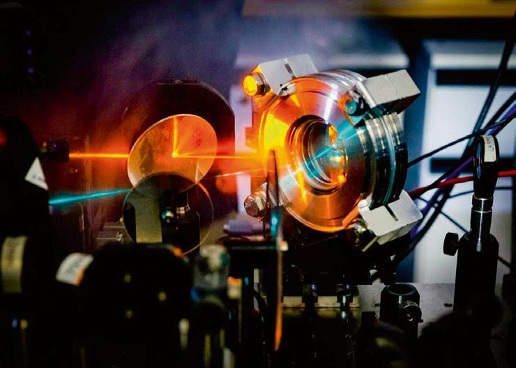
Limitations The fact that traditional MEMS testing is currently reaching its limits became clear at the Salland MEMS Seminar. The test specialist from Zwolle recently received international MEMS experts to discuss trends, challenges and solutions for future product generations. “With the growth of portable applications and systems that monitor people’s health at home, it’s now about technical challenges that ultimately decide on life and death,” said Nigel Beddoe of Cohu from Poway, California, maker of specialized MEMS testing equipment. “That means that designers of ICs, packaging, final testing and end applications need to work more closely together.”
Beddoe made it clear that Cohu is increasingly facing technical limitations in terms of test quality and productivity. He explained that for the most advanced microphones with a signal-to-noise ratio of 70 dB, there are actually no good tests – while 75 dB is already coming. Cohu supplies machines that test 0.8 mm by 0.8 mm MEMS parts with 256 pieces at a time. “This really puts us at the limit of what we can do,”
MEMS trends Accelerometers are one of the most common MEMS applications. In their traditional form, they consist of a mass suspended from springs. If this mass is moved by a physical stimulus, the resulting movement or vibration can be picked up in many ways: capacitive, piezoelectric, piezoresistive, thermal, optical or with tunneling. The toolkit of the MEMS designer seems infinite.
MEMS-based accelerometers were already used in airbag systems over thirty years ago, but nowadays, these sensors can also be found in drones, game consoles, mobile phones, sports watches, GPS devices, medical applications and much more. MEMS have evolved from stand-alone components to integrated six-axis and even nine-axis sensors.
The progress in MEMS technology is astonishing. While the first MEMS-based rotation sensors were able to detect a 1.5-degree rotation, now 0.1 degree is common, and 0.05 degrees is coming. Gyroscopes and e-compasses make grateful use of this accuracy. MEMS barometers had an accuracy of meters when they first came on the market, now 25 centimeters is normal. For MEMS microphones, a signal-to-noise ratio of 55 dB is the current standard and 70 dB is the absolute top, but for mobile phones, 75 dB is already in the works.
Two trends stand out. Due to the requirements for compactness and price, MEMS technology is increasingly being integrated into chips but also in advanced packaging. For example, Bosch is supplying a system-in-package with a three-axis 14-bit accelerometer, a three-axis 16-bit gyroscope and a three-axis geomagnetic sensor. All of this is packaged with a 32-bit microcontroller in a module measuring just 5.2 by 3.8 by 1.1 millimeters.
Credit: Rick Kloekke
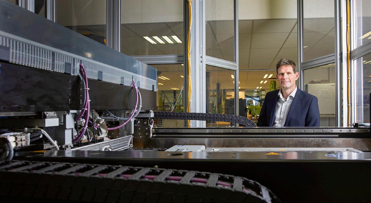
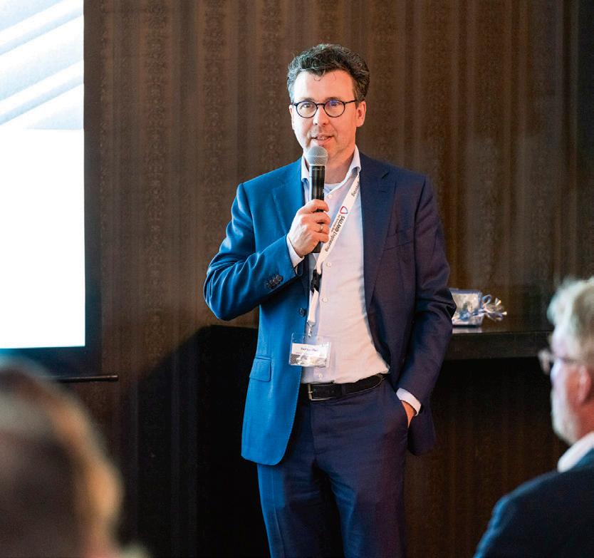
MEMS is a typical market Paul van Ulsen, CEO of Salland Engineering, likes to sink his teeth into.
Beddoe told the seminar audience. It’s also becoming increasingly common for MEMS components to be assembled without packaging. Beddoe: “It really is a big challenge to process these fragile die-level packages.”
Cohu made an urgent appeal in Zwolle. “IC designers continue to design smaller MEMS without much concern about how to test them in a 24/7 high-volume production environment. We should be at the table during design reviews, even before deciding on the size of the packages and how to properly stimulate them.” Beddoe noted that Cohu is also approaching the limits when it comes to achieving the accuracies that test specifications impose. “These limits also need to be taken into account in the design phase.”
The basic tooling MEMS is a typical market Paul van Ulsen, CEO of Salland Engineering, likes to sink his teeth into. It’s a niche that needs fast test solutions to validate chips at the end of the line. “We expect to almost halve the testing time,” says Van Ulsen, based on the results his company has shown with prototypes. In some cases, the test time can even be reduced to a fraction. “This month, we’re already validating chips for customers.” Van Ulsen expects to be able to deliver hardware early next year.
Salland Engineering is targeting these kinds of innovation in the test market. Before new ICs go into production, the specialists from Zwolle are already talking to chip manufacturers about developing technology to validate their circuits at the end of the line.
Van Ulsen doesn’t only deal with semiconductor manufacturers but also with suppliers of automatic test equipment (ATE) such as Advantest, Cohu (formerly LTX-Credence) or Teradyne. They provide the basic tooling: signal processing and robust computers for the analysis of the test data. These expensive test cells will last fifteen to twenty years, but due to the rapid progression of developments, they always need technology updates – something in which the Zwolle company is specialized.
Salland says it’s now ready to supply the power supplies, instrument modules, test programs, test protocols and interface hardware to enable the expansion of ATE equipment for MEMS. Current methods test MEMS components in their packaging with a physical impulse, for example, by tapping an acceleration sensor and measuring its response. According to Salland Engineering, this can largely be replaced by testing the chips with electrical signals while they’re still on the wafer. Wafer-level tests can be carried out to a high degree in parallel, which significantly increases the speed.
The major challenges with MEMS are to measure very small currents and capacities and to understand the physics. In any case, the measuring accuracy needs to go up considerably. “In the case of chips, we’re talking about microamps, whereas in the MEMS test process, it’s picoamperes and femtofarads – a thousand times smaller,” says Van Ulsen. “Also, MEMS components are sometimes less than a square millimeter in size. It requires a lot of new technology to be able to handle that.”
Two steps The majority of chip manufacturers still test their MEMS components with rack and stack equipment, ie self-built cells with standard instruments to test the sensors at an acceptable speed. Cohu is one of the few suppliers of specialized instruments based on physical tests. Van Ulsen thinks that Salland Engineering can complement this with its latest MEMS test technology. “Our aim is to no longer stimulate MEMS physically, but only electrically.”
The Salland CEO predicts that the MEMS test process will consist of two steps in the future. In the first step, chip manufacturers characterize their components with physical signals to validate the design. “If you know that the design is good and you know the characteristics of the sensor, then in high-volume production, you can limit yourself to process validation: is it right or is it wrong? In our opinion, this can be done entirely electrically, in parallel, at wafer level and to a large extent in packaged components: you then make a statement as to whether such a chip has been produced well enough. That ultimately reduces the testing costs.”
Van Ulsen does think that there will always be applications in the MEMS world that are so mission-critical that they’ll require physical tests. “The automotive industry will want 100 percent certainty and will probably not be so quick to switch to electrical testing alone. But even if you do it partly electrically and carry out random physical tests, you can reduce the test time by half or even more.”