13 minute read
How ASMI became the key supplier of semicon ALD equipment


Twenty years ago, a small Finnish company called Microchemistry held the key to continuing Moore’s Law. From twelve contenders, it picked ASM International to scale up – to the great delight of Intel.
Jorijn van Duijn
Advertisement
On 22 January 1999, a single visit radically overturned ASM International’s future. On that date, ASMI chief technology officer Ernst Granneman received two visitors from Finland: Kari Lampinen and Matti Ervasti. The former was a manager for mergers and acquisitions at a Finnish energy company called Fortum. The latter was a manager of a small subsidiary called Microchemistry, located in Espoo, Finland. Both men visited Bilthoven in order to find out whether ASMI was interested in acquiring Microchemistry and its technology.
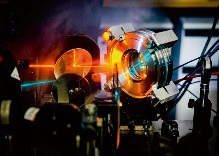
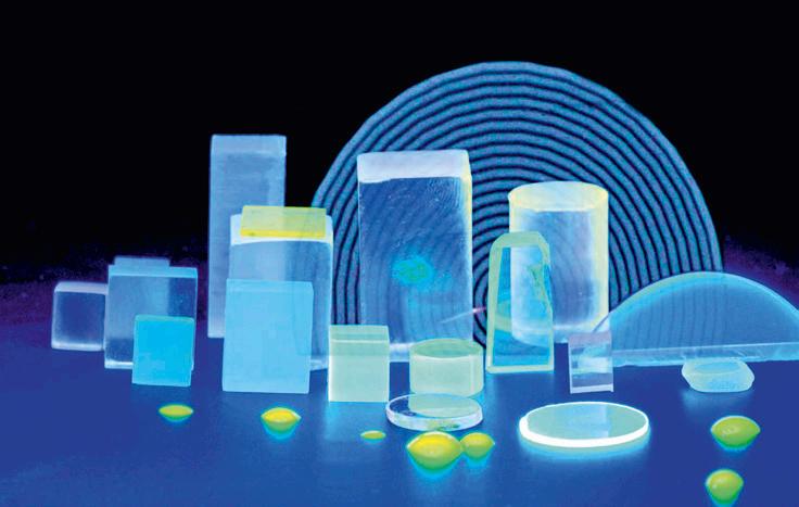
Their pitch was about atomic layer deposition (ALD), a process developed by the founder of Microchemistry. ALD entails the controlled deposition of films in layers of single atoms. The process enabled the formation of the thinnest films with unprecedented conformity and step coverage while offering low contamination of unwanted impurities. Through the prevalence of Moore’s Law, technologies enabling the construction of materials at the smallest dimensions – atoms in this case – enjoyed the particular interest of the chip industry. It was just a matter of time before ALD would become indispensable for further miniaturization.
At first sight, ALD has some resemblance to chemical vapor deposition (CVD). In the classical CVD process, two or more reactants form a film of the desired material by introducing them in the reactor at the same time. In an ALD process, however, the desired reactant gasses are inserted sequentially into a reaction chamber. Taking turns, the reactant gasses react with the exposed surface until all available bonds are saturated.
Crucially, in ALD, the chemical reaction on the exposed surface automatically stops after all the available sites of the surface have been ‘occupied’, causing the substrate surface to be ‘saturated’. Adding more reactants wouldn’t result in more reactant on the surface. This principle of self-saturation is critical and enables the sequential deposition of layers of the same or different composition.
After saturation, a purge of an inert gas like nitrogen or hydrogen removes possible reaction products and all the remaining or surplus reactant molecules in the chamber. Next, the second reactant is inserted, which reacts with the first reactant until – again – all available sites of the substrate have reacted. Once more, the remaining reaction products and the redundant reactant molecules are purged out of the reactor. This complete process, called a “cycle”, adds one layer to the thin film being deposited. This cycle can be repeated until the desired film thickness is obtained.
After IBM, Intel called Apart from the ALD process, the small Finnish company triggered the interest of Granneman with its treasure trove of processes. Over the course of many years, it had developed several pieces of equipment
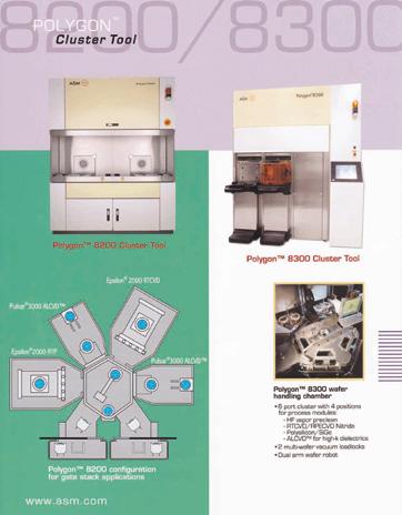
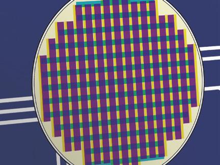
ASMI’s Polygon cluster tool was designed for gate stack manufacturing.
and various ALD chemistries. Through its tools, process knowledge and interactions with some chip manufacturers, Microchemistry singled out various applications in semiconductor production.
The most prospective was the gate stack. Microchemistry knew how to use ALD for the deposition of new exotic materials for the gate stack, for instance for the creation of high-k dielectrics and metal electrodes. By 1999, the first alteration of the CMOS gate stack in forty years of semiconductor manufacturing was already looming large on the horizon. It was this application that stirred the interest of chip manufacturers like Intel.
Microchemistry’s work on gate stack materials also perfectly aligned with ASMI’s work done in an earlier European research project and a joint development program with Siemens on integrated deposition processes in multi-chamber systems. Process and material-wise, Microchemistry’s techniques formed the missing piece. Moreover, some of its tools were designed according to the industry’s Material and Equipment Standards and Code (MESC). In other words, they could be integrated into multi-chamber tools developed by ASMI. All things fell in place.
One week later, after consulting ASMI’s founder and CEO Arthur del Prado, strategic marketing manager Chris Werkhoven, the newly appointed CTO Ivo Raaijmakers and resigning CTO Granneman e-mailed Lampinen to confirm ASMI’s interest in a joint future with Microchemistry. He argued that the technology clearly matched ASMI’s technology roadmap and that the company would fit in the ASMI organization. The organizational structure of ASMI as designed by Del Prado allowed the Finnish start-up to grow into an established original equipment manufacturer rather independently.
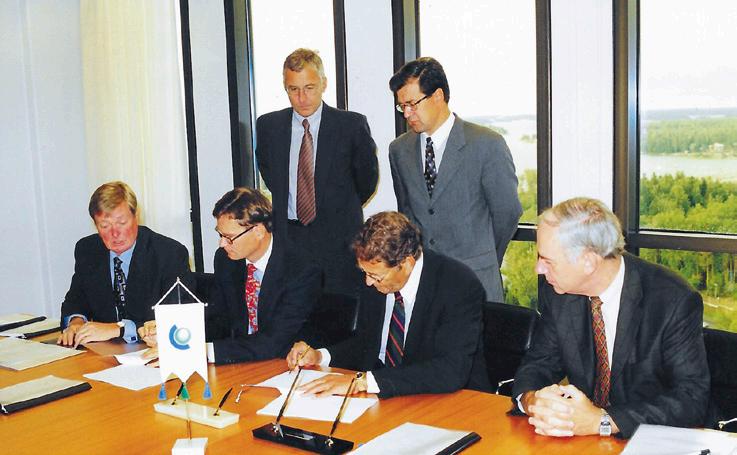
After the initial meeting in January, things moved fast, in particular within ASMI. Werkhoven and Granneman visited Microchemistry to learn about the technology. Del Prado, Granneman, and ASMI’s CFO Rinse de Jong worked out the financial details with Ervasti and Lampinen. By July, Del Prado and De Jong succeeded in finding “an acceptable creative financial solution” and finalized the acquisition. The firm was now called ASM Microchemistry.
In 1999, Microchemistry employed 42 staff, of whom 14 in development, 12 in engineering and 8 in manufacturing. It had four types of machines, including the F120 and the F200 for semiconductor production. The F120 was a mere R&D reactor, only capable of processing very small substrates and primarily meant for process development. The F200 was designed for semiconductor manufacturing. Technology development agreements were in place or
Sealing the deal: Arthur del Prado (seated, second on the right) signing the acquisition of Microchemistry.
were negotiated with Intel and IBM, while others, such as Imec, were considered.
Soon after the acquisition was finalized, positive signals were received. Major chip manufacturers congratulated ASMI after Werkhoven contacted prominent customers surrounding ASMI’s due diligence of Microchemistry. They had anxiously awaited the outcome of the acquisition process. “A few hours after they called. Also about Microchemistry, congratulating us they called a very good buy, quickly concluded and successful in competition with 12 (!) other contenders [sic]. So, a job well done,” Werkhoven faxed to headquarters.
Key supplier Chip manufacturers had a reason to be happy. As some Intel engineers involved in the process development of the gate stack later recalled in IEEE Spectrum, “For the first two years, all the dielectrics we tried worked poorly. (...) You want a transistor to operate exactly the same way every time it switches, but these gate stack structures behaved differently each time they were charged up. The results were very discouraging.”
“To make the dielectric layer, we were using one or two different semiconductor manufacturing techniques: reactive sputtering and metal-organic chemical vapor deposition. Unfortunately, both processes produce surfaces that, though remarkably smooth by most standards, were nevertheless uneven enough to leave some gaps and pockets in which charges could get stuck. We needed something even
smoother – as smooth as a single layer of atoms, actually.”
Depositing such thin films in a controlled manner wasn’t possible with any other method. Process-wise, ALD had the best papers, even though reproducible high-volume manufacturing still had to be established.
The acquisition of the rather unknown company and its novel technology set ASMI on a trail packed with uncertainties but with high expectations as well. The positive comments from customers, some of whom were the most advanced semiconductor manufacturers at the time, stimulated confidence in the path chosen. “The announcement of the intended acquisition has created a lot of positive momentum for ASMI from customers like Intel, IBM, Philips and STMicroelectronics. The combination of Microchemistry’s technology with ASMI’s global infrastructure solves the main issue from these customers that Microchemistry on its own was too small to support the technology and create a production-ready solution,” reported management to the somewhat skeptical supervisory board of ASMI. The Bilthoven company’s introduction in the process did place the decision-making on a different level at the customer. For ASMI, this was a very positive signal.
After the formalization of the acquisition of Microchemistry, it was up to ASMI’s management to capitalize on the momentum. A new approach had to be developed to enact the newly obtained ALD technology. The matter was quite urgent indeed. ASMI had been propelled to the lead in ALD and gate stack technology. Moreover, the major chip manufacturers were impatient. Moore’s Law defined the pace of their technological development and the gate stack constituted a rapid approaching obstacle on their route.
Microchemistry was a gift from heaven: unexpected, but most welcome. It was up to ASMI to fulfill its promise.
Jorijn van Duijn studied the history of ASM International over six years, relying upon interviews and Arthur del Prado’s personal archive. As a PhD candidate, he was affiliated with Rijksmuseum Boerhaave and Maastricht University. This article is an excerpt from his PhD dissertation entitled “Fortunes of high tech: a history of innovation at ASM International, 1958-2008”, which is now available at Techwatch Books.


Order now
Jorijn van Duijn explores the dynamics behind the greatest high-tech innovation: the computer chip. This brand new book describes the history of ASM International between 1958 and 2008.


Maarten Buijs is the R&D director at Moba.

Technology forecasting
Irecently bought a new TV for our living room. I was very pleased to be able to buy an affordable OLED television from Philips. Although the TV is manufactured by TP Vision, I assume that some or much of the technology inside originated from Philips. When I worked at Philips Research (Natlab), organic LEDs were hot and we started working on organic LED technology for displays, having missed the right boat for LCD and having failed with proprietary flat-panel technology based on electron hopping.
At the Natlab in Eindhoven, we worked on the polymer variant of OLEDs. I was heading the department responsible for the ink-jetting science and polymer OLED technology. Philips Research in Aachen worked on small-molecule OLED. I seem to remember that that was to our dismay because our technology assessment indicated polyLED to be superior. We didn’t believe in the concept of spending money on competing technology development. To my recollection, Aachen got away with it because their technology wasn’t for television but for lighting, which was their turf. Now we see that small-molecule OLED is the technology of choice for TV.
Another invention of that time was the CD-I, the interactive CD that Philips brought to the market when I started working there. Even though it was expensive, I felt compelled to buy it as an eager young Philips employee. I never regretted that: it was a perfect interactive experience at a time when game computers had terrible graphics and PCs still worked with command lines. My small children loved it and were still fondly reminiscing of it years later when Nintendo and other game consoles dominated.
Unfortunately, this was another textbook case of a bad go-to-market strategy. As a member of Philips’ Genootschap van Jonge Academen (“society of young academics”), I had volunteered to sell or at least explain
If the constituents of the philosopher’s stone were known, innovation would be a piece of cake
the new CD-I to customers in an electronics shop in the Netherlands. Together with the other volunteers, I was trained by people from Philips Nederland in how to approach this: focus on the educational value, with items like exploring the Smithsonian or Van Gogh’s paintings, and downplay the game capabilities of the CD-I, like battleship or pinball – very nice games that we still refer to in our family. None of the shoppers I subsequently talked to was interested in the former; most wanted to know more about the games. The CD-I never became a success but I still believe that the technologies it used were the front-runners in what is now, of course, a huge gaming industry.
Forecasting which promising technologies are going to make it and in what form is obviously the philosopher’s stone with which fortunes, empires and industries are built. If the stone’s constituents were known, innovation would be a piece of cake, though much less fun (and blood, sweat and tears). I do strongly believe in two important ingredients.
The first is having a champion who owns the technology and is willing to go all the extra marathons to turn it into a success. There are many examples of such champions in history. I often refer to the well-known story of James Dyson, partly because there’s also a link to my past at the Natlab: in my first job, I was asked to look at a patent and prototype for cyclone-based vacuum cleaning, developed by one of the engineers, at about the same time that Dyson was despairing to find a manufacturer for his similar solution. In the end, he managed to build an empire.
The second ingredient to the philosopher’s stone is the agile concept of failing fast. In a nondeterministic system, that’s the best way of quickly finding out what works and what doesn’t.
Both ingredients point away from large monolithic R&D organizations, like the Natbab, towards an ecosystem of fast and nimble start-ups. Just like other large corporations, Philips came to that realization, slimmed down its research organization and laid the foundation for Brainport by creating the High Tech Campus.