B a c kg r o u n d
Semicon
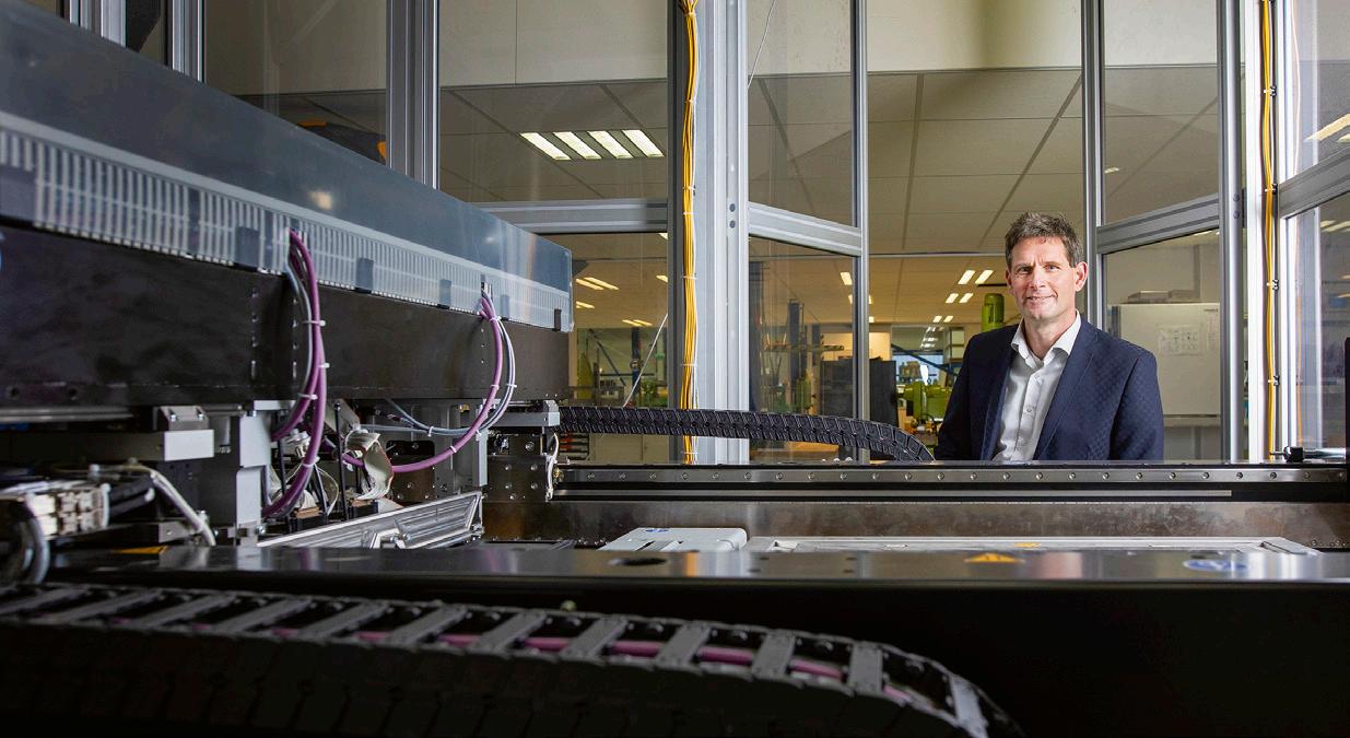
How ASMI became the key supplier of semicon ALD equipment Twenty years ago, a small Finnish company called Microchemistry held the key to continuing Moore’s Law. From twelve contenders, it picked ASM International to scale up – to the great delight of Intel. Jorijn van Duijn
O
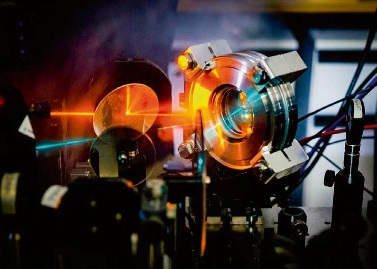
n 22 January 1999, a single visit radically overturned ASM International’s future. On that date, ASMI chief technology officer Ernst Granneman received two visitors from Finland: Kari Lampinen and Matti Ervasti. The former was a manager for mergers and acquisitions at a Finnish energy company called Fortum. The latter was a manager of a small subsidiary called Microchemistry, located in Espoo, Finland. Both men visited Bilthoven in order to find out whether ASMI was interested in acquiring Microchemistry and its technology. Their pitch was about atomic layer deposition (ALD), a process developed by the founder of Microchemistry. ALD entails the controlled deposition of films in layers of single atoms. The process enabled the formation of the thinnest films with unprecedented conformity and step coverage while offering low contamination of unwanted impurities. Through the prevalence of Moore’s Law, technologies enabling the construction of materials at the smallest dimensions – atoms in this case – enjoyed the particular interest of the chip industry. It was just a matter of time before ALD would become indispensable for further miniaturization. At first sight, ALD has some resemblance to chemical vapor deposition (CVD). In the classical CVD process, two or more reactants form a film of the desired material by introducing them in the reactor at the same time. In an ALD process, however, the desired re28
8
actant gasses are inserted sequentially into a reaction chamber. Taking turns, the reactant gasses react with the exposed surface until all available bonds are saturated. Crucially, in ALD, the chemical reaction on the exposed surface automatically stops after all the available sites of the surface have been ‘occupied’, causing the substrate surface to be ‘saturated’. Adding more reactants wouldn’t result in more reactant on the surface. This principle of self-saturation is critical and enables the sequential deposition of layers of the same or different composition. After saturation, a purge of an inert gas like nitrogen or hydrogen removes possible reaction products and all the remaining or surplus reactant molecules in the chamber. Next, the second reactant is inserted, which reacts with the first reactant until – again – all available sites of the substrate have reacted. Once more, the remaining reaction products and the redundant reactant molecules are purged out of the reactor. This complete process, called a “cycle”, adds one layer to the thin film being deposited. This cycle can be repeated until the desired film thickness is obtained.
After IBM, Intel called
Apart from the ALD process, the small Finnish company triggered the interest of Granneman with its treasure trove of processes. Over the course of many years, it had developed several pieces of equipment
ASMI’s Polygon cluster tool was designed for gate stack manufacturing.
and various ALD chemistries. Through its tools, process knowledge and interactions with some chip manufacturers, Microchemistry singled out various applications in semiconductor production. The most prospective was the gate stack. Microchemistry knew how to use ALD for the deposition of new exotic materials for the gate stack, for instance for the creation of high-k dielectrics and metal electrodes. By 1999, the first alteration of the CMOS gate stack in forty years of semiconductor manufacturing was already looming large on the horizon. It was this application that stirred the interest of chip manufacturers like Intel. Microchemistry’s work on gate stack materials also perfectly aligned with ASMI’s work done in an earlier European research project and a joint development program with Siemens on integrated deposition processes in multi-chamber systems. Process and material-wise, Microchemistry’s techniques formed the missing piece. Moreover, some of its tools were designed according to the industry’s Material and Equipment Standards and Code (MESC). In other words, they could be integrated into multi-chamber tools developed by ASMI. All things fell in place.