13 DECEMBER 2019 | 21 FEBRUARY 2020
Novioscan
Belly monitor ultrasounds ballooning bladders
8
BITS-CHIPS.NL
Grai Matter Labs Eindhoven design takes AI processing to the edge
WUBBO’S WINDING WATTAGE GENERATOR CATCHES WIND
Measure the World Around You Solutions to Condition Every Signal
Bridging the gap between the world we live in and the digital world is a complex task. Microchip’s standalone mixed-signal, linear and interface products enable designers to easily and accurately collect, measure, monitor and convert a wide variety of signals to improve your product designs. In addition to a wide variety of general-use products, we also have a selection of high-performance devices to help you meet your strict design requirements. Explore our options to condition your signals!
Explore your options at www.microchip.com/Signal
The Microchip name and logo and the Microchip logo are registered trademarks of Microchip Technology Incorporated in the U.S.A. and other countries. All other trademarks are the property of their registered owners. Š 2019 Microchip Technology Inc. All rights reserved. DS20006064A. MEL2244A-ENG-10-19
O
pinion EDITORIAL Paul van Gerven is an editor at Bits&Chips.
Self-driving in the dark
A
ccording to a US government report, the truck should have been visible for at least seven seconds, yet Joshua Brown did nothing to avoid a collision. And, crucially, nor did his Tesla, though Brown apparently trusted it to do so. The car had intermittently urged its occupant to take back control of the vehicle with visual and audio signals. Brown complied every time by putting his hands on the steering wheel, but only briefly, so as only to turn off the alarm. It cost him his life. The crash in 2016 kicked off a debate about the safety of Tesla’s self-driving features and the way the company goes about deploying them, which is still going on. While most car manufacturers now try to downplay expectations for autonomous driving, saying it will take at least another decade, Tesla is taking a much more aggressive approach. Elon Musk often makes rather bold claims about the capabilities of Tesla’s current self-driving technologies and even bolder promises about future features. Earlier this year, he predicted that his company would be able to start operating a fleet of driverless ‘robo-taxis’ by the end of 2020, for example. Tesla’s ‘release-it-now-fix-it-later’ approach to rolling out self-driving even prompted accusations that it’s using customers, such as Joshua Brown, as crash test dummies. By making the system seem more capable than it is and by not enforcing constant alertness of ‘drivers’, it’s putting lives at risk, some argue. (Currently, there are four confirmed Tesla Autopilot deaths in the US). Brown’s own family won’t have any of it, however. “We heard numerous times that the car killed our son.
That’s simply not the case. There was a small window of time when neither Joshua nor the Tesla features noticed the truck making the left-hand turn in front of the car. People die every day in car accidents. Many of those are caused by a lack of attention
At what performance level should we allow autonomous driving systems on the road? or the inability to see the danger. Joshua believed, and our family continues to believe, that the new technology going into cars and the move to autonomous driving has already saved many lives. Change always comes with risks, and zero tolerance for deaths would totally stop innovation and improvements,” said a statement released well over a year after the accident, after all official inquiries had been completed. Personally, I feel the blame primarily rests with Brown himself, but Tesla does share in it. It should have been more cautious and responsible, at the very least by disallowing hands off the wheel at this stage of technological development. Yet, as the Brown family argues, if autonomous driving is ever going to be a reality, we’ll probably have to accept some deaths caused by machine error in order to save many more lives in the long run.
The key question is this: at what performance level should we allow (partially) autonomous driving systems on the road? These systems will eventually drastically reduce the number of road accidents, but first, they need to rack up the miles to be perfected. If we proceed too cautiously, we might prevent accidents like Brown’s, but by delaying the advent of the autonomous driving era, there would be many more fatalities overall. If we proceed too brashly, the public backlash will probably result in more delays, and hence more deaths as well. So, there’s a fine balance to strike here, complicated by the fact that we simply don’t know how good the systems are at any point in time. That would take many (semi-)autonomous miles to assess. Basically, we’re self-driving in the dark. We’ll have to deal with it like approaching a blind junction: no point in coming to a full stop, but stepping on the gas would be foolish.
8
3
CONTENTS IN THIS ISSUE OF BITS&CHIPS
8
10
News
News
Wearable ultrasound from Nijmegen senses your ballooning bladder
Eindhoven-connected Grai Matter Labs edges to the AI market
Novioscan has successfully hit the market with its first product to measure bladder content from outside of the body.
GML’s Grai One is claimed to be the world’s first AI chip optimized for ultra-low-latency and low-power processing at the edge.
3 News
7 Noise 8 Wearable ultrasound from Nijmegen senses your ballooning bladder 10 Eindhoven-connected Grai Matter Labs edges to the AI market 15 Hot electrons give up the goods 16 Leydenjar’s silicon anode enters production realm
4
8
15
Self-driving in the dark
Opinion 3 13 21 31 38
Hot electrons give up the goods
Self-driving in the dark – Paul van Gerven The headhunter – Anton van Rossum Survival of the fIoTtest – Cees Links Technology forecasting – Maarten Buijs Today’s fish – Eppo Bruins
16
18
News
Background
Leydenjar’s silicon anode enters production realm
Kitepower sails toward energy transition
Start-up Leydenjar is setting up a pilot line in Eindhoven to prove its high-capacity battery anodes can be made not just in labs.
Inspired by Wubbo Ockels, Yes!Delft start-up Kitepower is flying kites in order to harness wind energy and convert it into usable power.
28
How ASMI became the key supplier of semicon ALD equipment
Background 18 22 24 28 32
Kitepower sails toward energy transition Placing and matching a multilayer chip antenna TU Delft material shines in medical detectors How ASMI became the key supplier of semicon ALD equipment Salland Engineering ready to accelerate MEMS testing
Interview
34 Building a foundation for the Dutch high tech ecosystem
8
5
“It keeps people fresh� Thermo Fisher software manager Reinier Perquin believes that providing his employees with training opportunities not only helps bring in new personnel, but it also keeps his people fresh. He finds that his colleagues come back with new ideas, new energy and new inspiration. Thermo Fisher Scientific, a multinational leader in biotechnology product development, employs more than 70,000 people around the world. thermofisher.com hightechinstitute.nl/software
NOISE
AI
Telecom
The greatest gift of the US people to the world is Black Friday. Not the commercial event per se, but the stream of video clips that entertain the more civilized parts of the planet every year. It’s nice to feel superior over the ’Merican riffraff fighting their ways into stores to get their grubby hands on some piece of 50 percent off hardware or jewelry that was doubled in price before it got discounted. Cyber Monday shoppers, too, may feel particularly smug when getting their package handed to them by the delivery guy. But don’t think for one second online shoppers don’t have to put up a fight. According to cybersecurity firm Radware ‘shopping bots’ are on the rise. They buy discounted or limited supply items and then sell them somewhere else at a markup. And since no human can compete with bots at filling out online forms, it really is a fight no ordinary shopper can win. PvG
If the US export ban on many tech products was meant to put China in its place, it may be failing, The Wall Street Journal suggested recently. The newspaper had access to a teardown analysis, which showed that Huawei’s flagship smartphone, the Mate 30, contains not a single US component. The post-ban phone has audio chips from NXP on board, for example, instead of Cirrus Logic in previous versions. The discovery shouldn’t come as a surprise, however, as analysis by Ars Technica on another highend phone showed that the Chinese phone makers actually already sourced most of their components from outside the US. Furthermore, a Huawei executive told Bloomberg that “the company has known [a US export ban] could be a possibility for many years. We’ve invested heavily and made full preparations in a variety of areas, including R&D and business continuity.” Clearly, hardware isn’t the problem for Huawei. Software and apps are an entirely different story, however. PvG
Top-15 semiconductor suppliers by revenue (in million dollars) Rank 2019 Rank 2018 1 2 2 1 3 4 4 3 5 5 6 6 7 7 8 8 9 9 10 10 11 15 12 11 13 13 14 12 15 14
Company Revenue 2019 2019/2018 (%) Intel 69,832 0 Samsung 55,601 -29 TSMC 34,503 1 SK Hynix 22,886 -38 Micron 19,960 -35 Broadcom 17,706 -3 Qualcomm 14,300 -13 TI 13,547 -9 Toshiba 11,276 -18 Nvidia 10,514 -12 Sony 9,552 24 ST 9,456 -2 Infineon 8,946 -3 NXP 8,857 -6 Mediatek 7,948 1 Top 15 314,893 -15
Huawei doesn’t need US hardware
RF
A blessing in disguise
The Netherlands-China Low-Frequency Explorer (NCLE) had to wait in space for over a year before being deployed. That was longer than planned, as the Chinese Queqiao satellite host took more time than anticipated to finish its primary mission, ie serving as a relay station for communications between a moon lander and terrestrial ground stations. The prolonged exposure to the coldness of space may have caused the NCLE’s three antennas to not deploy properly: while one extended to the full five meters, the other two only managed half of that. Not all is lost, however. NCLE’s primary mission Credit: Marc Klein Wolt, Radboud University
Tis the season to be shopping
Source: IC Insights
It’s a rather meager year in semiconductors, with IC Insights expecting a worldwide revenue decline of 13 percent in 2019. The top-15 fares a little worse even, with revenue dropping two points more. Only three companies manage to register year-over-year growth: Sony, TSMC and Mediatek. Only Sony manages to really impress, though, with revenue expected to increase 24 percent thanks to surging image sensor sales. NXP registers a 6-percent sales decline this year, which compared to its top-15 peers is middle-of-the-road. However, the average is strongly affected by the strong downturn in the memory industry, with growth rates ranging from -18 to -38 percent. Excluding memory makers, NXP finds itself at the lower end of the spectrum. PvG
Credit: Huawei
NEWS
was to observe the Sun and Jupiter at low frequencies. This cannot be done from Earth because the ionosphere absorbs this part of the EM spectrum. But the research teams also hoped to pick up signals from when the first stars were born in the universe, or even from before that. For this objective, the shorter-than-intended antennas are actually a boon: they’re more sensitive to the particular frequencies associated with the “Cosmic Dawn”. PvG 8
7
NEWS HEALTHCARE
Wearable ultrasound from Nijmegen senses your ballooning bladder In 2014, a urologist from Twente needed a solution to measure bladder content from outside of the body. The answer: an external wearable ultrasound device. Now, the first product has successfully hit the market, with a follow-up expected in early 2020. CEO Rob Tweehuysen and CTO Reinout Woltjer explain how Novioscan created the Sens-U Kids. Jessica Vermeer
W
hen giving children incontinence training, there are two main choices for the trickiest cases. Either provide the child with a timely alarm or put a moisture sensor in their diaper. The drawback, however, is that neither solution will teach the child to cope without an aid. The Nijmegen-based start-up Novioscan has developed an ultrasound device that enables external monitoring of the bladder. The small, wireless wearable can be positioned on the lower abdomen. With ultrasound, it’s able to measure the total bladder volume. At 80 percent, the device vibrates, notifying the child to go to the bathroom.
Credit: Novioscan
Twente and Utrecht
Five years ago, Novioscan originated from another Nijmegen company, Noviotech. The inspiration came from Ger Dijkman, a urologist from Twente. He was looking for a solution to externally measure the content of the bladder. Research showed that this was a common question in his field and an untapped market. Dijkman’s idea was to use ultrasound to detect bladder volume. Together with Jan-Jaap Koning, Jeroen Langevoort and Rob Tweehuysen, he decided to start his own company. At a Health Valley assembly, the foursome presented their plans. As it turned out, urologist Pieter Dik from the University Medical Center Utrecht (UMC) and medical entrepreneur Huibert Tjabbes 8
8
were looking into a similar problem. In Twente, the main focus was to gain insight into how the bladder fills and empties under normal circumstances. In Utrecht, they were working on incontinence training for children that had followed multiple trainings already. They wanted a method to give biofeedback at 80 percent bladder volume. The two sides quickly realized there was an opportunity for collaboration. They co-founded Novioscan and secured a license agreement with the UMC. The hospital was able to offer valuable support, as it was perfectly equipped to help such initiatives. There were budgets available for spin-off activities and support with clinical research.
Sens-U Kids
Since the bladder just grows with fluid volume, a device was built to determine how big the organ is. “Our Sens-U Kids product generates an ultrasound pulse, looks at the reflection from the front and back wall of the bladder and the time difference between the two. That difference is then converted into millimeters using the speed of sound,” explains Novioscan CTO Reinout Woltjer. “From six to eight measuring points in one plane, the volume is then calculated.” Though the Sens-U Kids is capable of monitoring every second, it’s typically used to measure bladder content twice a minute. There’s an option to set a maximum thresh-
and energy-efficient design. The battery has about 10-20 percent the capacity of a mobile phone battery. Woltjer: “We claim it lasts for 24 hours, but practically, it’s about 4 or 5 days.”
Next generation
Credit: Novioscan
old, to which the measured volume is compared. Once this level is reached, a warning will be issued – usually at 80 percent. The alarm is then repeated with increasing strength until the bladder is emptied. The device uses Bluetooth Low Energy to connect to a smartphone. By utilizing the Novioscan-developed app, users can set the maximum volume and get help positioning the system on the lower abdomen. After this, the solution works autonomically. This essentially solves the questions posed in both Twente and Utrecht. An additional benefit of the Sens-U Kids device is the option to create a bladder diary, which is of great value for diagnostics, treatment and evaluation of treatments.
Minimum viable product
The greatest challenge for a wearable device is that it needs to work with a tiny battery. Mainstream ultrasound equipment, like the
Bladderscan by Verathon, has a plug and needs a nurse to operate it. In addition, a medical CE marking requires validation of all claims made about what the device can do. That’s why Novioscan chose to initially aim for a minimum viable product. “We wanted to hit the market as soon as possible,” says Woltjer. “Our only claim is that the device can measure bladder content. In reality, it may be used for incontinence training, but we left that out in our initial CE application. With the CE marking, the product can be applied in several hospitals for clinical tests, giving us valuable user information, which we could use to develop the next generation.” Although some examples showed children to successfully remain dry after removing the device, Novioscan is far away from clinically proving such functionality. Development work for the Sens-U Kids mainly focused on creating a simple, cheap
Novioscan is now working on a follow-up product, which is set to be released in the first quarter of 2020. Co-founder and CEO Rob Tweehuysen: “The new product will be more compact and comfortable to wear for children in wheelchairs. The functionality will be exactly the same but with an upgraded design. It will be 35 percent smaller and more rounded. This means we don’t need another CE review.” As soon as the new product is released, the old one will be taken off the market. For now, the Sens-U Kids is a standalone system. All data is stored within the device. A physician can download everything in one go. In principle, the system could develop into a data collection device as well. But, as Woltjer points out, “Going to the cloud would mean meeting numerous privacy demands.” The next generation will truly take things to the next level and will require a new CE application. Tweehuysen: “That device needs to work for adults as well, which is medically more challenging. The bladder is positioned deeper inside the body and the shape varies more, as does the BMI index of the person wearing it.” The target group will be elderly people in nursing homes. The current product does work for adults, but not nearly good enough. The development will, therefore, start from scratch again.
Generate cash
Currently, all turnover comes from doctors and hospitals. “A minimum viable product was a deliberate choice. We can get useful feedback from medical staff, which is what we need right now,” says Woltjer. The product is sold for 900 euros. Going to larger volumes, the price will naturally go down. Financially, Novioscan is not yet ready for the next step. “We first need to generate cash,” notes Tweehuysen. Woltjer adds: “In the long term, we want to have a technology platform that can be used for different applications. To be and stay top-of-the-bill, maybe until we can insert ultrasound devices within the body.” 8
9
NEWS ARTIFICIAL INTELLIGENCE
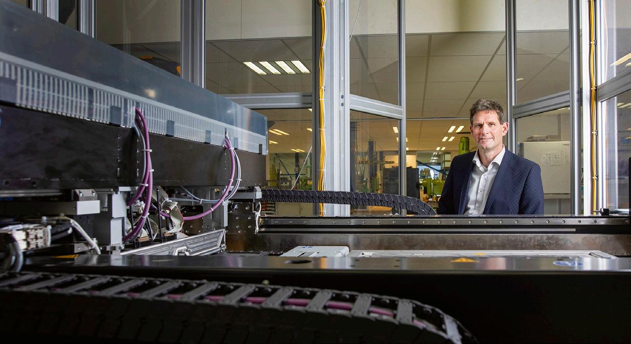
Eindhovenconnected Grai Matter Labs edges to the AI market Having operated under the radar for almost two years, Grai Matter Labs recently stepped into the spotlight, announcing its first products. According to the fabless semiconductor scale-up with Eindhoven roots, Grai One is the world’s first AI chip optimized for ultra-low-latency and low-power processing at the edge. It’s based on the company’s brain-like Neuronflow architecture. Nieke Roos
C
ompared to the human brain, standard computer CPUs are terribly inefficient. With their classical Von Neumann architectures, they’re constantly moving data around, back and forth between the central processing unit and central memory, thereby squandering lots of power. No wonder companies such as Grai Matter Labs (GML) are venturing to create neuromorphic, ie brain-like, processors. GML’s technology is based on 20 years of breakthrough research on the human brain carried out at the Vision Institute of the former Pierre and Marie Curie University in Paris (now part of Sorbonne University). The fabless semiconductor company’s neuromorphic computing paradigm overcomes
10
8
the limitations of standard CPUs. Grai One, GML’s recent hardware debut, like the brain, uses a large number of local compute elements called neurons and impulses called spikes for data communication, offering massively parallel and fully programmable sensor analytics and machine learning at reduced power consumption. According to GML, its Grai One is the world’s first AI chip optimized for ultra-low-latency and low-power processing at the edge. It’s targeted at response- critical edge applications in autonomous navigation, human-machine interaction and smart healthcare markets. “Grai One processes edge AI applications orders of magnitude faster than traditional architec-
tures while maintaining a power footprint suitable for battery-powered devices,” explains GML CEO Ingolf Held.
Silicon Hive
GML started out as Brainiac, incubated in 2016 within the iBionext healthcare startup studio in Paris. Among its founders are Vision Institute professor Ryad Benosman, iBionext chairman Bernard Gilly and Atul Sinha – a team combining experiences in neuromorphic computing, silicon design and entrepreneurship. In December 2017, the company closed its Series-A financing round of 15 million dollars, led by iBionext, and in April of last year, it adopted its current name. Next to its HQ in
Credit: Grai Matter Labs
Under the (technological) leadership of Ingolf Held (left) and Menno Lindwer (right), GML has been quietly building its team and product portfolio. Credit: Grai Matter Labs
The fully digital Grai One chip measures 20 mm2 in TSMC 28nm technology.
the French capital, it has offices in Silicon Valley (San Jose) and Eindhoven. The Dutch connection comes from co-founder Sinha, a prominent figure in the high tech industry in the Netherlands. After having worked at Philips for 13 years, he was the long-time CEO of spin-off Silicon Hive, which was acquired by Intel in 2011. He went on to become one of the founding fathers of the Eindhoven University of Technology medical robotics startups Preceyes and Microsure. At present, he serves in the board of directors of several Dutch high tech companies, including IoT security specialist Intrinsic ID and healthcare monitoring expert Sensara. Intel’s decision, at the end of 2017, to terminate the former Silicon Hive team located at the High Tech Campus Eindhoven boosted GML’s Dutch presence. Although the American semiconductor behemoth backtracked on its plan a couple of months later, much of the ‘harm’ was already done: by then, several of the 115 employees had moved just around the corner to the newly formed office of the AI start-up, brought together by their former boss Sinha. Among them were Ingolf Held and Menno Lindwer, who were appointed CEO and VP Engineering, respectively.
Under Held and Lindwer’s (technological) leadership, GML has been quietly building its team and product portfolio. With Paris and Silicon Valley focusing more on machine learning applications and business development, Eindhoven is responsible for architecture exploration, hardware design and AI tools. This culminated in the introduction of the Neuronflow programmable processor technology and the Graiflow software development kit last September and the Grai One chip at the end of October.
35 mW and 20 µs
Neuronflow draws from neuromorphic and dataflow paradigms to solve core problems for real-world AI applications. The technology is designed for multiple types of computation: digital signal processing, machine learning inference, procedural computation and mixtures of these. One of its breakthroughs is dynamic dataflow processing of real-time data, which drastically reduces application latency. The underlying architecture utilizes in-memory compute with a mesh of cores and local neuron/synapse memories, avoiding the memory bottleneck of
the traditional Von Neumann model. The neuron cores process 8 or 16-bit data, are event-triggered and connected through a packet-switched network-on-chip. By only processing and propagating the sparse change events, the system has much less work to do and uses much less power. Based on Neuronflow, the fully digital Grai One chip measures 20 mm2 in TSMC 28nm technology and implements a mesh of 196 neuron cores with local memories for a total of 200,000 neurons. It provides a GPIO interface to offload latency-critical AI workloads. At 100 percent neuron core utilization, the chip consumes as little as 35 mW and has a latency as low as 20 µs. For keyword spotting, the latency was benchmarked below 3 µs, while for hand gesture recognition, it was even below 1 µs. Neuronflow and its future silicon implementations are supported by GML’s Graiflow SDK. It’s capable of both conventional program execution and machine learning computation via industry- standard languages like Tensorflow, Python and C++. The kit includes a graphical editor, compute and network APIs, a mapper, a simulator, a debugger, a code generator and full runtime support. 8 11
11 MARCH 2020 VERKADEFABRIEK ’S-HERTOGENBOSCH
SAVE THE DATE
BITS&CHIPS
MACHINE LEARNING CONFERENCE
Powered by
CALL FOR PAPERS
MLCON.NL
#BCML20
O
pinion
THE HEADHUNTER Anton van Rossum anton.van.rossum@ir-search.nl
Ask the headhunter B.A. asks: E.M. asks: For about ve years been About two fiyears ago, now, I tookI’ve a job as a senior engineerdyat aworking project as manager at chip a promising, the semiconductor division With of a large namic high tech start-up. our Korean technology really R&D team, we face acompany. number ofI major like it there,First although my challenges. of all,I’ve we reached have to get peak in technology the organization. To apersonal wildly complex ready for move ahead, I really to speak market in no time. The need next challenge Korean and that seemstechnical impossible is to recruit sufficient exwith my limited language skills. perts to develop the products. Because I’mmonths ready forafter the next step Just a few I joined, in myengineering career, I’m talking to an Amerthe manager left the ican company the later, Netherlands. company. Not in much a couTheyofoffkey er me a challenging role in an ple engineers followed suit. interesting segmentwere and Because notechnology other candidates my enthusiasm is growing every available, I offered to take on day. the We’re currently theunfamiliarity negotiation position, despiteinmy phasethe fortechnology. the contract. with I didn’t have many One of my tasks wasconcerns to attractabout suitthe salary. company able experts.I assumed This has the proved to be would makeSilicon me a suitable er based impossible. Valley off is the only on my experience, skill can set be and the hotspot where engineers found cost of living the Netherlands. To who have the in specific knowledge we simplify Unfortunately, matters, I listedasmy require. youcurrent know, income components with the salaries over there arethe so gross high and net amounts. All in all, I get that it would be a miracle to get peo-a net toannual salary of 92,500 euros, ple come to the Netherlands. including benefimy ts such as has a freemade furAs a result, team nishedprogress. apartment, pay,mananlittle No gratuity thanks to nual airlinewho tickets to my country agement, didn’t support us of at birth the costs my daughter’s all in and achieving ourofobjectives. This international Toago my surprise, changed a fewschool. months when an I received aand muchexperienced lower offer: consul80,000 expensive eurosfrom per year (30 percent fatant the net US was hired totax solve cility), but no problems. apartment and none of the technical theLast other special ts Isurprise, now have.I week, to benefi my big I’minvited tryingtotoa convince the compawas meeting with HR. In to increase their offer. I’veinformed sent my anyshort conversation, they contract with my terms ofbeemployme that my contract would termiment, and a taxthat declaration and all calnated I was suspended. A culations, including comparisons of few days later, I received a settlement the cost ofcontract living intermination the Netherlands proposal: withversus Korea, butmonths, I’ve not made much in one and a half a 6-months progress yet. Perhaps we can can-
cel my participation in the pension supplement to the unemployment scheme,and which would reference. win me a gross benefit a positive 800 eurosam perI month. What What supposed to else do can withI do to convince match this? The teamthe hascompany already to been inmy current formed thatsalary? I won’t be coming back, so returning to them seems unrealThe headhunter answers: istic to me. Skipping participation in a collective pension is impossible; it’s mandatory. The headhunter answers: The overview you’ve provided shows Given your short employment perithatthe your current employer has a od, offer isn’t that bad. Howevverythecomplete package of benefi ts er, whole process leaves a lot to to attract asbe desired.and Youretain can’ttop be talent. blamedI for sume this is one of the reasons why
You’re better You’ll have tooff looking forward judge your ‘golden and learning handcuffs’ onfrom their the truepast merits you lack accepted the offerYou to work Kothe of progress. didn’tinhave rea a few years to ago. Nowthe that you’ve enough budget attract required reached the in your lacked career and experts andceiling you yourself the your child is to school, you’ll knowledge to going lead the team technihave to judge these ‘golden handcuff s’ cally – which was sufficiently known onmanagement. their true merits. As you’ve indito They gave you hardly cated, the social life for you and your any guidance in your important task partner isn’t very exciting because and no critical feedback whatsoever youyour don’t speak Korean in on performance. Still,and thelife team a city millions was in of your hands. like Seoul will get bored in athelegal longpoint run. of view, your From Although it’s quite company doesn’t haveunderstandable a case. In the to takelegal yoursystem, current the salary as will the Dutch court starting point for a possible transfer, only terminate your contract if you you’ll alsonotice need to be realistic. I’m and not received well in advance ruling possibility thatopporthere if you out werethe given sufficient are companies in Europe that can oftunity to improve. In addition, a disfer youfor a higher salary, but you have missal poor performance must be to find them first. I’m aware of top
salaries atmotivated Intel, Broadcom and Qualproperly and documented comm, they’re located in much in orderbut to stand a chance. more expensive Iregions andwouldn’t they’re Nevertheless, definitely not in the ‘hiring Of course, recommend such amood’. procedure. It will you can companiesenergy in Silicon only leadfind to negative and Valley where yourbetter qualities slander. You’re off certainly looking would beand appreciated, but getting forward learning from the past.a workcould visa there is almost impossible. You have gone to management You’ll have make a choice, also and raised theto issue about the lack of weighing in theguidance quality of life of your resources and much earlier. family and your market further iscareer in Besides, the labor definitetechnology. monly favorable If foryou youchoose at the the moment. ey, you’ll keep you’ll on searching. With yourhave trackto record, have no There willfinding be no increase thiswithin bid. problem anotherinjob two or three months. Regarding the settlement, I’d consider asking for an extra month of pay – you have a two-month cancellation period. The supplement to 100 percent of your last-earned salary for a period of six months is very reasonable. Under current law, you’re not even entitled to a transition allowance within two years of starting your employment. New rules will come into effect on 1 January 2020, stipulating that from then on, you’re entitled to a gratuity payment for every six months of employment, regardless of whether you’re dismissed or you resign yourself.
11 85 13
ORDER NOW
“ASML’s Architects is an impressive book, a curious book and a book for the curious. (…) Clearly a labour of love by Raaijmakers but nonetheless an easy read.” Peter Clarke, eeNews, February 1, 2019 “Rene Raaijmakers’ book on the history of ASML is a monumental work in its depth and breadth from ASML’s beginning through 1996. (…) No tech company’s history has ever been covered to such a degree.” Dan Hutcheson, The Chips Insider, February 1, 2019
techwatchbooks.nl/architects
NEWS SOLAR
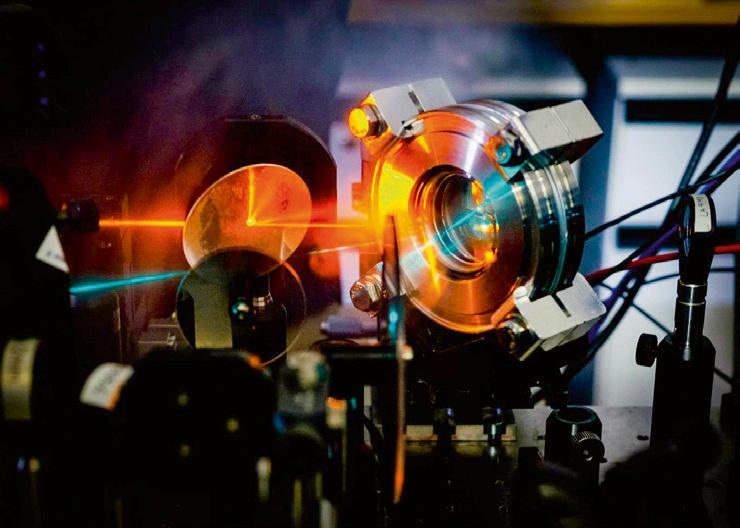
Hot electrons give up the goods Harvesting the energy of so-called hot electrons in perovskites is surprisingly easy, suggests a study by the University of Groningen and Nanyang Technological University. The finding may help to increase the efficiency of perovskite solar panels. Paul van Gerven
the excited electron and then swiftly transferred to crystal lattice vibrations. In other words: the excess is lost as heat. Key to capturing the energy of so-called hot electrons is slowing down the energy loss to the lattice, so as to at least have a chance of capturing some of it. This has proven extremely challenging, as a complex interplay of disparate processes is involved. The best results have been obtained with nanoparticles, which feature fewer ‘energy sinks’ than bulk materials. The study led by RUG researcher Maxim Pshenichnikov provides a proof of principle that hot electrons in perovskites can be captured. In fact, merely stacking the p erovskite with an organic compound called bathophenanthroline (bphen) and exciting the perovskite’s electrons to energy levels just
above bphen’s bandgap resulted in a remarkably smooth transfer of said electrons to the organic compound. Spectroscopic analysis confirmed that the transfer to bphen is much faster than the undesirable cooling process. This doesn’t mean we should expect beefed-up perovskite solar cells anytime soon, though. In the experiment, the researchers made sure they only excited perovskite electrons, whereas, in the real world, both the inorganic and organic would absorb light to generate both hot and cold electrons (which have little excess energy). It remains to be seen whether the hot electrons can be extracted without sacrificing the cold ones. “This underscores the complexities of realizing practical hot- carrier perovskite solar cells,” the researchers conclude in Science Advances.
Credit: NTU Singapore
T
he performance of perovskite solar cells has improved spectacularly over the past decade. In 2009, an efficiency of 3.8 percent for a single-junction cell was reported but the current record already stands at 25.2 percent – right behind the best silicon devices. Being a thin-film technology, however, perovskite solar cells will be significantly cheaper to produce and hence are expected to give silicon a run for its money – though perovskites and silicon can reinforce one another as well. It’s no coincidence that the top efficiencies of perovskites and silicon are very close. The maximum efficiency of a ‘regular’ single-junction solar cell is 31-33 percent, depending on the bandgap. As designs, materials and processing techniques are optimized, any single-junction solar cell will approach that limit. For both silicon and perovskites, the low-hanging fruit simply has been picked. That’s why researchers have turned their attention to more advanced concepts. Understandably, they’ve set their sights one of the major sources of energy loss in solar cells: the excess energy that photons have with respect to the semiconductor’s bandgap, which is lost as heat. As it turns out, it may be easier to capture that energy portion in perovskites than in silicon, researchers from the University of Groningen (RUG) and Nanyang Technological University Singapore show in Science Advances.
Hot and cold
Whenever a photon strikes a semiconductor, an electron is excited only when the photon’s energy is equal to or higher than the bandgap. If its energy is smaller, no photoexcitation occurs and the photon passes right through the device. If its energy is larger, the excess is ‘absorbed’ by 8 15
NEWS BATTERIES
Leydenjar’s silicon anode enters production realm Start-up Leydenjar is setting up a pilot production line in Eindhoven to prove its high-capacity battery anodes made from nano-textured silicon can be made not just in labs but in factories as well.
A
sked to look back at 3.5 years of developing a new anode recipe for lithium-ion batteries, Christian Rood of Leydenjar prefers to answer what outsiders have told him. “Experts and people from the battery industry say we should be happy with the progress we’ve made. Personally, I would have liked to have seen a little more. I guess I’m not easily satisfied,” the company co-founder admits. In any case, it’s fair to say: so far, so good. Leydenjar, named after the battery’s predecessor, thanks its existence to technology that was developed many years ago at solar cell research institute ECN. Researcher Wim Soppe theorized that nano- texturing would improve the performance of thin-film silicon solar cells. He then successfully developed a plasma-enhanced chemical vapor deposition (PECVD) process to create a layer of silicon nano-pillars on a substrate. Unfortunately, they didn’t perform as well as hoped. The technology was shelved and almost forgotten until Soppe learned that silicon is a superior host for lithium ions, yet fails miserably as a battery anode because it can’t handle the mechanical stress associated with repeatedly taking in and letting go of guests. The porous structure of pillared silicon might be able to handle that, Soppe figured. This time, he was onto something. In fact, the lithium-loading capacity of his silicon approaches the theoretical limit, without getting damaged by loading and unloading lithium. Fast forward to today, Leydenjar is gearing up to prove its technology can be mass-produced. The ultimate goal: making anodes for lithium-ion batteries that outperform the traditional graphite ones, without adding cost. 16
8
Credit: Leydenjar
Paul van Gerven
Order processing Roll-to-roll
Between the initial lab experiments and looking into manufacturing, a lot of work has been done. One important obstacle was layer thickness. “For proof-of-principle experiments, 200 nanometer is fine, but as an anode in a commercial battery, it needs to be 50 times thicker. Otherwise, it wouldn’t be able to generate a high enough capacity per area,” Rood explains. Another delicate task was selecting the battery’s electrolyte. Rood: “In a battery, a solid electrolyte interface is formed on the electrodes after a short period of operation. This film’s characteristics depend on the electrolyte and can affect battery performance substantially. We needed to find a good match for our anode.” Leydenjar successfully increased layer thickness and identified a proper electrolyte, allowing the company to pair the anode with a suitable cathode and start building actual batteries. Their prototype promptly won the BMW Start up Challenge, providing Leydenjar with an opportunity to present their technology to key executives and developers of the car manufacturer. “It got us quite a lot of exposure as well. We received calls from various battery and car companies,” says Rood. That kind of attention is a big help when trying to round up additional funding, which Leydenjar secured in March 2018. “This money we used to optimize the energy density of the anode. Our silicon has tenfold the capacity compared to graphite, leading to a 50 percent higher energy density in the battery.” “We also started working on our production process, because we won’t be selling batteries but rather the manufacturing equipment for our anodes – along with know-how, of course. Our PECVD tools need to seamlessly fit into existing production infrastructure without adding cost.” Both these items have been ticked off from Leydenjar’s list. Next up is proving all this still holds at actual production volumes. “This is why we’re setting up a roll-to-roll pilot production line in Eindhoven now (the anodes use copper foil as a substrate, PvG). In addition, this will allow us to engage with potential customers and partners on a larger scale. In fact, we’re already working with an OEM and battery manufacturer to develop prototype battery cells.”
SEARCH, CHECK STOCK, TRACK, PURCHASE
made easy
A better buy
Apart from the pilot line, Leydenjar is also setting up its own battery lab in Leiden, which will develop battery recipes tailored to different applications. Initially, the start-up targets specialized niche markets, after which it will work its way up to consumer products, to ultimately penetrate the holy grail of battery markets: automotive. Each successive application is more demanding, eg pertaining to battery life. “We aim to ship our first fully optimized modules to customers in 2021,” states Rood. Will Leydenjar still be a company on its own by then? “I expect we’ll have partnered up with a company in the battery industry. We’re becoming a better buy with every step we take, so sooner or later, an offer should present itself.”
Simplify your purchasing with our custom productivity tools nl.mouser.com/servicesandtools
Genuine traceable components
Simple Buying Solutions
Ready-to-ship inventory
8 17 Buyer Tools-95x235-4mmbleed-nl-buyers.indd 1
21.08.19 10:06
B a c kg r o u n d
Energy
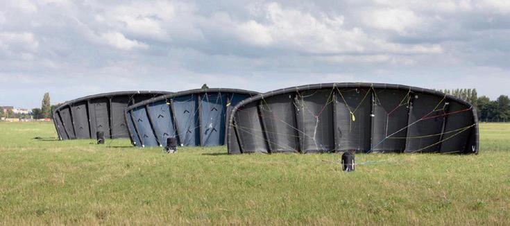
Kitepower sails toward energy transition As the energy transition gets wind beneath its wings, one Yes!Delft start-up is drawing inspiration from Dutch astronaut and professor, the late Wubbo Ockels. Its solution: fly kites in order to harness wind energy and convert it into usable power. Credit: Kitepower, CC BY-NC-ND
Collin Arocho
A
fter becoming the first Dutchman to go to space, Wubbo Ockels began working as a professor of aerospace engineering at Delft University of Technology (TU Delft). In 1997, inspired by a friction burn he received while flying his kite, O ckels applied for a patent on a technology that could harness the energy of the wind and convert it into usable power. Just a year later, he was awarded the first-ever patent on laddermill technology – a kite- controlled, airborne turbine that can collect and store energy from the blowing wind. In 2004, Ockels founded the kite power research group at TU Delft. The unit was designed to tackle scientific challenges like aerodynamics and automatic flight control of the tethered wing structure, as well as to design efficient generators to store the collected power. In 2016, after several years of technology development and product design, Kitepower was spun out of the university, lifting off with CEO Johannes Peschel holding the string. His goal: to bring this inexpensive and highly mobile system of clean energy generation to the market.
Pump action
Fundamentally, the Kitepower system is a relatively simple concept. A kite is attached to a long lead line made from dyneema – a lightweight, ultra-strong material. Ideally, this line will fly the kite a few hundred meters in the sky to catch the best wind. Going too high, however, would have a deleterious effect, as the increased drag on the line would hinder its performance. The dyneema lead is wound around and connected to a drum winch on the ground. 18
8
The kites come in various sizes, 40, 60 and 100 m2, and are made from a super-light material, similar to that found in the sailing world.
When the sail takes off in the wind, the attached line is then pulled with it, turning the drum and driving a generator to create energy. Once deployed to a specified length, the kite is tilted out of the direct wind stream and reeled in by the turning winch. After being hauled in, the kite is tipped into the wind current and again pulled out by the force of the wind, completing this cycle repetitiously to create power. “It acts similar to a glider. We tip the kite and pull it back in very quickly. By doing this repeatedly, we’re actually creating energy through this pumping action,” explains Kitepower technical manager Joep Breuer. “While reeling back in, we’re using less than 10 percent of the energy that’s created from being pulled out. To be honest, the energy use is actually not the problem at all. The biggest obstacle is the time we use, because that’s time we’re not able to produce power, so we have to buffer.”
wind, in a cross wind, allowing it to go faster. As the speed of a kite increases, there’s a quadratic rise in the pulling force of the string, which yields more energy from the generator. To maintain this optimal path, Kitepower has developed a kite control unit, which utilizes motors to adjust the pitch and direction of the sail, maximizing efficiency and power production. “This kite control unit works much the same ways as a kitesurfer. It has two main motors, one to steer left and right and the other one to adjust the pitch to very quickly control the lift and drag on the kite,” describes Breuer. “We’ve also implemented GPS systems and a series of sensors to determine the position and orientation of the kite. This unit holds the intelligence of the system and can independently decide where the kite will fly, while we monitor on the ground through a wireless downlink.”
Kitesurfing
Despite the potential of this clean-energy solution, there’s still much to be determined. While the company’s first systems are being planned for deployment in Curacao in 2021, currently, the 20-man Kitepower team is
To generate maximum power, the engineers at Kitepower have adopted a specific flight path for the kite – a figure eight. This keeps the kite flying perpendicular to the
Replace mass with intelligence
Credit: Kitepower, CC BY-NC-ND Credit: Kitepower, CC BY-NC-ND
Attached to a long lead line, the Kitepower kite will fly a few hundred meters in the sky to catch the best wind.
points. First, are the physical properties of the Kitepower system. The kites themselves come in various sizes, 40, 60 and 100 m2, and are made from a super-light material, similar to that found in the sailing world. The only difference is the addition of an inflatable support structure to assist in taking off. This is a staggering 95 percent reduction in mass and materials, which equals a reduction in cost. Second, the entire system can be completely contained within a standard 20-foot shipping container, which allows for an unparalleled
potential for mobility as the kite-powered solution can be loaded up on a truck and moved for deployment. “I often say that we replace mass with intelligence. With our computer-optimized flight-path technology, we’re able to adjust and find the best wind in order to extract maximum energy – something a massive wind turbine will never be able to offer,” emphasizes Breuer. “Right now, we’re developing a 100-kilowatt version that should produce about 450 megawatt hours of electricity every year. That’s enough to power around 150 Dutch households on an annual basis.” Credit: Kitepower, CC BY-NC-ND
still in the testing phase of its business development. But as engineers are out test- driving the system at the Valkenburg airfield, a growing number of the conventional wind turbines are popping up and spinning freely across the European landscape. Once installed, these massive fans can last for decades and are able to turn 24/7 in unmanned operation – a feat that will prove to be an uphill battle for the young company. However, notwithstanding these obstacles the Yes!Delft start-up believes it has some very attractive and unique selling
The lead line is wound around and connected to a drum winch on the ground, which creates power from the kite’s movement. 8 19
Quality literature for the high tech
Philips Natlab – Kraamkamer van ASML, NXP en de cd
Paul van Gerven and René Raaijmakers describe the research lab in great detail and make its impact on the technological world visible. Persistent myths such as the lab’s hailed freedom are dismantled. € 39,50
On techwatchbooks.nl, you can find exciting books on technology
O
pinion
IOT Cees Links is a Wi-Fi pioneer, founder and CEO of Greenpeak Technologies and currently General Manager of Qorvo’s Wireless Connectivity business unit.
Survival of the fIoTtest
W
inning an Olympic gold medal begins with good genes, they say. But good genes can only do so much. Even people born with exceptional abilities and talents must still work very hard to become the best. Only with the proper amount of quality training – certainly not too little, but also not too much – can someone become the best. This is where technology comes in: it can help to maximize the training efforts. Today’s IoT technology for fitness monitoring and integrated applications is a great help to push that extra mile, to gain that extra second or to lose that extra pound. Let’s take a closer look at a day in the life of a professional cyclist and the applications that support her. First thing in the morning, the instant Alicia opens her eyes, she’ll tap her Fitbit and check her pulse at rest. Great cyclists generally have an extraordinary heart capacity, and a lower heart rate at rest typically implies efficient heart function and good cardiovascular fitness. It can also indicate if there are any infections or circulatory problems. This morning, our athlete has a very low heart rate, 37 beats per minute – all clear for a good training day. She starts off with a well-balanced breakfast of granola, fruit and yogurt for a total of 550 kcal. She enters the food and its weight in a food calculator app and shares it via the IoT with the nutritionist who’s part of her athletic support team. The nutritionist then optimizes Alicia’s food intake for the required output, based on three types of days: training, racing or rest. When it’s time to start her training session, our cyclist will put on
her training clothes, shoes and helmet. Her equipment is optimized by technology and the IoT: her smart helmet has bone conduction audio technology, which turns audio into
The IoT has a nice growth path in sports vibration that goes straight to the inner ear from the tabs of the helmet straps, through the cheekbones, bypassing the eardrum. The result is amazing: Alicia can hear music and voice navigation ‘inside her head’, yet still hear the ambient sounds of traffic to maintain situational awareness for safety. It’s the safest way to listen to music while riding. Once on her training ride, Alicia uses a power meter – a device fitted to the bike that measures the power output of the rider – and a heart rate meter to quantify her workout and give instant feedback. These measurements, along with GPS coordinates and speed, are broadcast as a live stream of sorts, so her trainer can keep track of everything in real time. In the past, trainers could calculate the average speed during training sessions and that was about it. Today, they look at distance and speed, power output and explosivity, velocity, resistance or help from tail or headwind, and many other variables. This allows for a much better evaluation of the session, which helps to maximize performance. In a world where every meter or second counts, people are likely to
jump at the opportunity to optimize their efforts. Indeed, the IoT has a nice growth path in sports. But for the rest of us, who aren’t professional athletes, connected IoT devices and applications can yield similar benefits. We can use different apps and wearable devices like a Fitbit or Apple Watch to track our own fitness, monitor progress toward goals, share our achievements and stay motivated, as well as convey information to healthcare providers. At its heart, the IoT can bring more information and more data for sports and health – no matter your fitness level.
8 21
B a c kg r o u n d
Wireless
Placing and matching a multilayer chip antenna How to get the maximum performance from a multilayer chip antenna with respect to antenna placement on a PCB and effective impedance matching? Würth Elektronik’s Muhammad Ali Khalid and Richard Blakey explain. Muhammad Ali Khalid Richard Blakey
T
he trend to miniaturize wireless communication devices has led to decreased PCB sizes and increased component densities. Although this shift has aided many areas of electronic design, it constrains RF front-end design. Due to the nature of antennas sending and receiving electromagnetic signals, they interact and are affected by the entire surrounding environment and are extremely sensitive to electromagnetic fields. This can be extremely problematic for RF engineers when integrating into a design an antenna that’s small, has good gain and efficiency in the frequency range of operation and is able to work as desired in different PCB environments. Multilayer chip antennas are an interesting choice for engineers who are restricted by cost and space requirements in wireless system design. Such antennas are formed from several layers of dielectric material, which are pressed and fired together into a monolithic structure. Each dielectric layer has patterned metallization on the surface that connects to other layers through vias. The inner conductors and vias form a radiating, multilayer meander structure, allowing the component to be smaller than a monopole antenna while achieving comparable performance. Electromagnetic fields are generated by the currents on the inner conductor.
PCB placement
When incorporating an antenna into an electrical product, some of the most critical stages of product development are the PCB layout and the design of device enclosures. This is 22
8
due to PCB component density continuously being increased to reduce the size of the device while not impairing the function of the design. Antennas can be extremely sensitive to power and ground planes when functioning as a λ/4 monopole antenna system. However, if the feedline and ground plane dimensions are carefully and intelligently taken into consideration when designing a chip antenna PCB, performance comparable to a λ/2 dipole antenna can be achieved. The positioning of the multilayer chip antenna is critical to achieving optimum gain and performance. Not following the design rules can significantly reduce the gain. Generally, the closer a grounded conductive material is positioned to the antenna, the lower the performance will be. The PCB corner is usually the most desirable location. This typically results in better
antenna gain as there’s only ground plane on two sides. When it’s not possible to place the antenna on the corner, it may go on the side of the PCB where it’s surrounded on three sides by ground plane, although the performance may be reduced. In extreme cases, the antenna may be positioned over or between ground planes. However, it must be noted that having any metal plate or battery above or below the antenna will also result in significant performance degradation. In some cases, there’s no other alternative except to utilize the area above or below, so careful consideration must be taken during the design and prototype stages to ensure sufficient antenna gain performance. Special considerations should be taken into account when an antenna is placed in an enclosure. Completely encasing it in
Simulated S-parameters of the WE-MCA multilayer chip antenna Internal structure of the WE-MCA multilayer chip antenna
metal is out of the question since the majority of the power from the antenna will be reflected back into the device. Housing made of non-conductive materials, such as plastic and glass, are much easier to incorporate into a design than conductive materials. Although the power isn’t reflected, the impedance and overall performance will be effected. Depending on the non-conductive material permittivity and proximity to the antenna, a significant frequency shift of up to hundreds of MHz can be expected. This needs correcting with appropriate impedance matching.
Impedance matching
Usually when a chip antenna is designed, the electrical specifications are measured on a manufacturer’s test board, in free space. In reality, an antenna will be operated in an environment that results in an impedance transformation, regardless of whether it’s intended or not. The impedance mismatch will be different for every device. Return loss is a good measure of how well an antenna is matched to its feed line.
This measure quantifies the amount of power being reflected back to the source. In an ideal world, a perfectly matched antenna would transmit 100 percent of the incident power with 0 percent return loss. Since no components are ideal, there are always undesired losses. A return loss of 10 dB is acceptable, meaning 90 percent power transfer, while 20 dB is equivalent to 99 percent power transfer. Impedance matching is carried out to mitigate mismatches caused by board placement, the surrounding components and enclosure and the presence or absence of overlapping ground planes. A capacitance or an inductance needs to be added to an antenna circuit to ensure the voltage and current are in phase. This minimizes the amount of reflected power and reduces the voltage standing wave ratio (VSWR), meaning maximum power transfer to and from the antenna by the feed line. During PCB design, special space needs to be allocated for a matching network for RF inductors and/or capacitors, the values of which need to be determined and
optimized during the prototyping stage. Matching networks are implemented as close to the load or source as possible, as the length of the feed line will have an effect on the impedance matching and power transfer. At microwave frequencies, the input impedance changes with respect to the
For the WE-MCA, the ground planes must be a minimum of 6 mm above or below the antenna area.
distance from the source, unless the transmission line is matched to the load/source with the characteristic impedance. The impedance can be assessed with the help of vector network analyzers (VNAs). VNAs are able to measure the amplitude and phase angle of a system. The measurements can be displayed in a number of formats but scattering parameters (S- parameters) and the Smith chart are the most useful tools when matching the impedance of an antenna. Muhammad Ali Khalid is a product manager and Richard Blakey is an application engineer, both at Würth Elektronik. Edited by Nieke Roos
Simulated surface current of the WE-MCA at a frequency of 2.45 GHz 8 23
B a c kg r o u n d
Materials
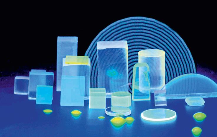
TU Delft material shines in medical detectors You may not know it, but a type of material called scintillators was probably involved when you had your last medical scan. Working with the French company Saint-Gobain, scintillator expert Pieter Dorenbos at Delft University of Technology is currently developing the next generation of these materials. Jessica Vermeer
W
hilst rushing towards airport security, everyone will undoubtedly zigzag their way through a bunch of queue poles with belts that make out the waiting lines before the actual security check. Once you’ve passed these lines, you’re probably not aware that you’ve already been checked for radioactivity. Some of the queue poles in airports contain detectors for radioactivity. This is, of course, to prevent travelers from carrying radioactive material onto the plane. It’s one of many applications for a special type of material, called scintillators. Scintillators are capable of absorbing ionizing radiation from a radioactive particle and convert its energy into a short pulse of visible light. This is why they can be used to build excellent radiation detectors: even a tiny bit of radiation produces a light pulse, which is easily detected using an electronic light sensor. The principle is not only useful at airports but also in hospitals: both PET and CT scanners always rely on scintillating materials. Pieter Dorenbos of Delft University of Technology (TU Delft) has been researching scintillators for 30 years now. In fact, he was there when the research group was founded, not long after then research leader Carel van Eijk realized how useful these materials can be. This is aptly illustrated by the fact that Dorenbos’ Luminescence Materials research group in Delft has been collaborating with Saint-Gobain for over 20 years now. The French company 24
8
is specialized in the production of glass and crystals. “Those crystals are supplied to companies that build detectors. SaintGobain also builds detectors themselves,” says Dorenbos. The partnership is currently focusing on developing crystals that outperform existing crystals.
Co-doping
In PET scans, radioactive material is injected into the patient and the emitted radiation is used to put together a scan of a body part. The job of the scintillator is to catch the radiation and transform it into a short flash of light. The shorter and stronger the A set of luminescent scintillating crystals. Credit: Delft University of Technology
flash, the better, because such a well-defined event is easier to work with than a weak and ‘stretched out’ light signal. The nature of the scintillator has a strong influence on the type of light flash. A scintillator consists of a crystalline base material in which a radiation- absorbing and light-producing element is embedded. One of the better combinations is the base material CsBa2I5 (cesium, barium, iodine) with a little europium added. Europium absorbs the radioactive radiation quite well, but it also self-absorbs the light it emits, causing less light to leave the crystal. As the crystal becomes larger, this
Scintillators by TU Delft and Saint-Gobain
Delft University of Technology (TU Delft) is connecting with French glass producer Saint-Gobain to invent new scintillators for next-generation radiation detectors. TU Delft’s participation in this project is co-funded by Holland High Tech, Top Sector HTSM, with a public-private partnership grant for research and innovation. hollandhightech.nl effect increases – and that’s no good when you want to build a detector. Dorenbos’ latest research focused on the combination of europium (Eu) and samarium (Sm). Co-doping with samarium could effectively bend the disadvantage of europium into an advantage. This idea was applied to CsBa2I5. “Our idea was to add samarium, as it can absorb the light of europium and then emit it as a different color. In fact, samarium absorbs in the visible and emits in the invisible near-infrared, which makes the scintillator completely black.” The europium-samarium combo works well: the best result so far shows that it has a
resolution of 3.2 percent, which is quite high. The best resolution to date, 2.2 percent, was achieved with another material also discovered within the TU Delft research group of Dorenbos. “The europium-samarium material has the potential to beat that. It can go below 2 percent. It could take another five years but it does have that much potential.” Another advantage of samarium co-doped crystals is that the silicon-based infrared detectors aren’t affected by a magnetic field, which is important for 2-in-1 scanners, such as those that combine PET and MRI.
Collaboration with industry
The results in Delft are good news for SaintGobain. Several of the company’s successful products are based on the record-holding scintillator but that was invented 20 years ago and the patent is about to expire. Dorenbos: “The research on co-doping with samarium has potential, so they patented the material. By investing in research, Saint-Gobain can stay ahead of competitors. Whether the material actually ends up in a product is for them to decide. When the photon leaves the crystal, the work of our
research group is done. What happens next is up to someone else.” The combination of public and private funding is remarkable, especially for a topic that could be defined as fundamental research. “We do try to understand what’s happening, that’s fundamental. The interaction between high-energy radiation and the material, ionization, free electrons and holes: all of those aspects require complicated models to simulate. We need to know what’s happening to make the right choices in materials.” In the end, fundamental, empirical and applied research are combined to find an application. There’s much to be improved upon the samarium co-doped scintillating material. Samarium could also be used in a material that could potentially generate more photons. Dorenbos hopes in a year a follow-up research project will be up and running with two PhD students.
High Tech Highlights
A series of public-private success stories by Bits&Chips
A cerium-doped lanthanum chloride scintillator in a quartz vial. Credit: Delft University of Technology
8 25
DISCOVERY ON STAGE
Almost all primary schools in the Netherlands have an end-musical tradition: at the end of their last year, pupils perform a grand musical for their schoolmates, parents and families. At the Discovery Factory, a program has been developed for combining the musical project with STEAM (science, technology, engineering, arts and mathematics) education.
S
Science and technology education is often considered extra work for school teachers. Extra work in a field they don’t feel familiar with. But if you ask them if they feel comfortable leading the musical project for the 8th graders, their answer is mostly very positive. If you dive a bit deeper into the matter, you’ll find that there’s a lot of technology and crafts involved in musicals. Audiovisual technology, building the set, setting up the lighting, project planning, graphic design and communication using computer software, costume tailoring and more creative elements like dance and choreography – the musical is loaded with STEAM. Tutorial for tutors For teachers who want to explore the possibilities of integrating STEAM education into the musical project, the Discovery Factory
team, together with five primary schools in the city of Eindhoven, has developed a set of tutorials with several special tools. These can be used when executing a musical project with a school class, for instance, for designing and setting up all backstage technology. This enables children who don’t consider themselves to be the star actors to shine as well during the making of and all the action behind the curtain. All talents are rewarded in the end. On stage! Free download If you have aspirations in enthusing the school children in your region for science and technology, or the company you work for has, the “Discovery on stage” project could be your starting point! Download the tutorials on discoveryfactory.nl and convince the schools. If you need assistance, you can always call on our professionals for help.
The Discovery Factory is there to inspire youngsters for a future in design and technology. Projects are supported by tech companies such as ASML, Brainport Industries, Daf Trucks, Frencken Europe, Hager, NTS Group, Philips, Stam en De Koning and VDL Group, and by Bits&Chips as the media partner.
discoveryfactory.nl
B a c kg r o u n d
Semicon
How ASMI became the key supplier of semicon ALD equipment Twenty years ago, a small Finnish company called Microchemistry held the key to continuing Moore’s Law. From twelve contenders, it picked ASM International to scale up – to the great delight of Intel. Jorijn van Duijn
O
n 22 January 1999, a single visit radically overturned ASM International’s future. On that date, ASMI chief technology officer Ernst Granneman received two visitors from Finland: Kari Lampinen and Matti Ervasti. The former was a manager for mergers and acquisitions at a Finnish energy company called Fortum. The latter was a manager of a small subsidiary called Microchemistry, located in Espoo, Finland. Both men visited Bilthoven in order to find out whether ASMI was interested in acquiring Microchemistry and its technology. Their pitch was about atomic layer deposition (ALD), a process developed by the founder of Microchemistry. ALD entails the controlled deposition of films in layers of single atoms. The process enabled the formation of the thinnest films with unprecedented conformity and step coverage while offering low contamination of unwanted impurities. Through the prevalence of Moore’s Law, technologies enabling the construction of materials at the smallest dimensions – atoms in this case – enjoyed the particular interest of the chip industry. It was just a matter of time before ALD would become indispensable for further miniaturization. At first sight, ALD has some resemblance to chemical vapor deposition (CVD). In the classical CVD process, two or more reactants form a film of the desired material by introducing them in the reactor at the same time. In an ALD process, however, the desired re28
8
actant gasses are inserted sequentially into a reaction chamber. Taking turns, the reactant gasses react with the exposed surface until all available bonds are saturated. Crucially, in ALD, the chemical reaction on the exposed surface automatically stops after all the available sites of the surface have been ‘occupied’, causing the substrate surface to be ‘saturated’. Adding more reactants wouldn’t result in more reactant on the surface. This principle of self-saturation is critical and enables the sequential deposition of layers of the same or different composition. After saturation, a purge of an inert gas like nitrogen or hydrogen removes possible reaction products and all the remaining or surplus reactant molecules in the chamber. Next, the second reactant is inserted, which reacts with the first reactant until – again – all available sites of the substrate have reacted. Once more, the remaining reaction products and the redundant reactant molecules are purged out of the reactor. This complete process, called a “cycle”, adds one layer to the thin film being deposited. This cycle can be repeated until the desired film thickness is obtained.
After IBM, Intel called
Apart from the ALD process, the small Finnish company triggered the interest of Granneman with its treasure trove of processes. Over the course of many years, it had developed several pieces of equipment
ASMI’s Polygon cluster tool was designed for gate stack manufacturing.
and various ALD chemistries. Through its tools, process knowledge and interactions with some chip manufacturers, Microchemistry singled out various applications in semiconductor production. The most prospective was the gate stack. Microchemistry knew how to use ALD for the deposition of new exotic materials for the gate stack, for instance for the creation of high-k dielectrics and metal electrodes. By 1999, the first alteration of the CMOS gate stack in forty years of semiconductor manufacturing was already looming large on the horizon. It was this application that stirred the interest of chip manufacturers like Intel. Microchemistry’s work on gate stack materials also perfectly aligned with ASMI’s work done in an earlier European research project and a joint development program with Siemens on integrated deposition processes in multi-chamber systems. Process and material-wise, Microchemistry’s techniques formed the missing piece. Moreover, some of its tools were designed according to the industry’s Material and Equipment Standards and Code (MESC). In other words, they could be integrated into multi-chamber tools developed by ASMI. All things fell in place.
One week later, after consulting A SMI’s founder and CEO Arthur del Prado, strategic marketing manager Chris Werkhoven, the newly appointed CTO Ivo Raaijmakers and resigning CTO Granneman e-mailed Lampinen to confirm ASMI’s interest in a joint future with Microchemistry. He argued that the technology clearly matched ASMI’s technology roadmap and that the company would fit in the ASMI organization. The organizational structure of ASMI as designed by Del Prado allowed the Finnish start-up to grow into an established original equipment manufacturer rather independently. After the initial meeting in January, things moved fast, in particular within ASMI. Werkhoven and Granneman visited Microchemistry to learn about the technology. Del Prado, Granneman, and ASMI’s CFO Rinse de Jong worked out the financial details with Ervasti and Lampinen. By July, Del Prado and De Jong succeeded in finding “an acceptable creative financial solution” and finalized the acquisition. The firm was now called ASM Microchemistry. In 1999, Microchemistry employed 42 staff, of whom 14 in development, 12 in engineering and 8 in manufacturing. It had four types of machines, including the F120 and the F200 for semiconductor production. The F120 was a mere R&D reactor, only capable of processing very small substrates and primarily meant for process development. The F200 was designed for semiconductor manufacturing. Technology development agreements were in place or Sealing the deal: Arthur del Prado (seated, second on the right) signing the acquisition of Microchemistry.
were negotiated with Intel and IBM, while others, such as Imec, were considered. Soon after the acquisition was finalized, positive signals were received. Major chip manufacturers congratulated ASMI after Werkhoven contacted prominent customers surrounding ASMI’s due diligence of Microchemistry. They had anxiously awaited the outcome of the acquisition process. “A few hours after they called. Also about Microchemistry, congratulating us they called a very good buy, quickly concluded and successful in competition with 12 (!) other contenders [sic]. So, a job well done,” Werkhoven faxed to headquarters.
Key supplier
Chip manufacturers had a reason to be happy. As some Intel engineers involved in the process development of the gate stack later recalled in IEEE Spectrum, “For the first two years, all the dielectrics we tried worked poorly. (...) You want a transistor to operate exactly the same way every time it switches, but these gate stack structures behaved differently each time they were charged up. The results were very discouraging.” “To make the dielectric layer, we were using one or two different semiconductor manufacturing techniques: reactive sputtering and metal-organic chemical vapor deposition. Unfortunately, both processes produce surfaces that, though remarkably smooth by most standards, were nevertheless uneven enough to leave some gaps and pockets in which charges could get stuck. We needed something even
smoother – as smooth as a single layer of atoms, actually.” Depositing such thin films in a controlled manner wasn’t possible with any other method. Process-wise, ALD had the best papers, even though reproducible high-volume manufacturing still had to be established. The acquisition of the rather unknown company and its novel technology set ASMI on a trail packed with uncertainties but with high expectations as well. The positive comments from customers, some of whom were the most advanced semiconductor manufacturers at the time, stimulated confidence in the path chosen. “The announcement of the intended acquisition has created a lot of positive momentum for ASMI from customers like Intel, IBM, Philips and STMicroelectronics. The combination of Microchemistry’s technology with ASMI’s global infrastructure solves the main issue from these customers that Microchemistry on its own was too small to support the technology and create a production-ready solution,” reported management to the somewhat skeptical supervisory board of ASMI. The Bilthoven company’s introduction in the process did place the decision-making on a different level at the customer. For ASMI, this was a very positive signal. After the formalization of the acquisition of Microchemistry, it was up to ASMI’s management to capitalize on the momentum. A new approach had to be developed to enact the newly obtained ALD technology. The matter was quite urgent indeed. ASMI had been propelled to the lead in ALD and gate stack technology. Moreover, the major chip manufacturers were impatient. Moore’s Law defined the pace of their technological development and the gate stack constituted a rapid approaching obstacle on their route. Microchemistry was a gift from heaven: unexpected, but most welcome. It was up to ASMI to fulfill its promise. Jorijn van Duijn studied the history of ASM International over six years, relying upon interviews and Arthur del Prado’s personal archive. As a PhD candidate, he was affiliated with Rijksmuseum Boerhaave and Maastricht University. This article is an excerpt from his PhD dissertation entitled “Fortunes of high tech: a history of innovation at ASM International, 1958-2008”, which is now available at Techwatch Books. Edited by Paul van Gerven
8 29
Order now
Jorijn van Duijn explores the dynamics behind the greatest high-tech innovation: the computer chip. This brand new book describes the history of ASM International between 1958 and 2008.
techwatchbooks.nl/fortunes
O
pinion
INNOVATION Maarten Buijs is the R&D director at Moba.
Technology forecasting
I
recently bought a new TV for our living room. I was very pleased to be able to buy an affordable OLED television from Philips. Although the TV is manufactured by TP Vision, I assume that some or much of the technology inside originated from Philips. When I worked at Philips Research (Natlab), organic LEDs were hot and we started working on organic LED technology for displays, having missed the right boat for LCD and having failed with proprietary flat-panel technology based on electron hopping. At the Natlab in Eindhoven, we worked on the polymer variant of OLEDs. I was heading the department responsible for the ink-jetting science and polymer OLED technology. Philips Research in Aachen worked on small-molecule OLED. I seem to remember that that was to our dismay because our technology assessment indicated polyLED to be superior. We didn’t believe in the concept of spending money on competing technology development. To my recollection, Aachen got away with it because their technology wasn’t for television but for lighting, which was their turf. Now we see that small-molecule OLED is the technology of choice for TV. Another invention of that time was the CD-I, the interactive CD that Philips brought to the market when I started working there. Even though it was expensive, I felt compelled to buy it as an eager young Philips employee. I never regretted that: it was a perfect interactive experience at a time when game computers had terrible graphics and PCs still worked with command lines. My small children loved it and were still fondly reminiscing of it
years later when Nintendo and other game consoles dominated. Unfortunately, this was another textbook case of a bad go-to-market strategy. As a member of Philips’ Genootschap van Jonge Academen (“society of young academics”), I had volunteered to sell or at least explain
If the constituents of the philosopher’s stone were known, innovation would be a piece of cake the new CD-I to customers in an electronics shop in the Netherlands. Together with the other volunteers, I was trained by people from Philips Nederland in how to approach this: focus on the educational value, with items like exploring the Smithsonian or Van Gogh’s paintings, and downplay the game capabilities of the CD-I, like battleship or pinball – very nice games that we still refer to in our family. None of the shoppers I subsequently talked to was interested in the former; most wanted to know more about the games. The CD-I never became a success but I still believe that the technologies it used were the front-runners in what is now, of course, a huge gaming industry. Forecasting which promising technologies are going to make it and in what form is obviously the philos-
opher’s stone with which fortunes, empires and industries are built. If the stone’s constituents were known, innovation would be a piece of cake, though much less fun (and blood, sweat and tears). I do strongly believe in two important ingredients. The first is having a champion who owns the technology and is willing to go all the extra marathons to turn it into a success. There are many examples of such champions in history. I often refer to the well-known story of James Dyson, partly because there’s also a link to my past at the Natlab: in my first job, I was asked to look at a patent and prototype for cyclone-based vacuum cleaning, developed by one of the engineers, at about the same time that Dyson was despairing to find a manufacturer for his similar solution. In the end, he managed to build an empire. The second ingredient to the philosopher’s stone is the agile concept of failing fast. In a non- deterministic system, that’s the best way of quickly finding out what works and what doesn’t. Both ingredients point away from large monolithic R&D organizations, like the Natbab, towards an ecosystem of fast and nimble start-ups. Just like other large corporations, Philips came to that realization, slimmed down its research organization and laid the foundation for Brainport by creating the High Tech Campus.
8 31
B a c kg r o u n d
MEMS
Salland Engineering ready to accelerate MEMS testing The world doesn’t seem to be able to get enough of micromechanical sensors. However, the chip industry currently lacks the test technology when it comes to high-volume production of MEMS. Salland Engineering wants to change this by 2020. René Raaijmakers
M
icroelectromechanical systems (MEMS) have experienced a real triumph in recent decades. Invisibly, but steadily, they’ve penetrated almost every application that requires information from its environment. For highly specialized applications, discrete, customized MEMS sensors are already being utilized. But in some cases, the technology can also be integrated on CMOS chips. This allows MEMS to meet the high demands of the largest market, ie consumer electronics: compact dimensions, low costs and increased functionality. Navigation, height measurement and the current trend in movement tracking during sports – it’s all done utilizing information provided by MEMS sensors. The technology is no longer limited to the automotive industry. In the 90s, MEMS were a big hit in acceleration sensors for airbags. Nowadays, they’re much more widely used. Movement, pressure, light, moisture, sound and ultrasound – it can all be measured with micromechanical technology. The market for MEMS sensors is expected to continue to grow by more than 10 percent a year, based on trends such as the Internet of Things and people’s insatiable hunger to gather information about their environment and health. Research agency Yole predicts that the MEMS market will reach 100 billion dollars in 2023. In 2018, this was 62 billion dollars.
Limitations
The fact that traditional MEMS testing is currently reaching its limits became clear 32
8
at the Salland MEMS Seminar. The test specialist from Zwolle recently received international MEMS experts to discuss trends, challenges and solutions for future product generations. “With the growth of portable applications and systems that monitor people’s health at home, it’s now about technical challenges that ultimately decide on life and death,” said Nigel Beddoe of Cohu from Poway, California, maker of specialized MEMS testing equipment. “That means that designers of ICs, packag-
MEMS trends
ing, final testing and end applications need to work more closely together.” Beddoe made it clear that Cohu is increasingly facing technical limitations in terms of test quality and productivity. He explained that for the most advanced microphones with a signal-to-noise ratio of 70 dB, there are actually no good tests – while 75 dB is already coming. Cohu supplies machines that test 0.8 mm by 0.8 mm MEMS parts with 256 pieces at a time. “This really puts us at the limit of what we can do,”
Accelerometers are one of the most common MEMS applications. In their traditional form, they consist of a mass suspended from springs. If this mass is moved by a physical stimulus, the resulting movement or vibration can be picked up in many ways: capacitive, piezoelectric, piezoresistive, thermal, optical or with tunneling. The toolkit of the MEMS designer seems infinite. MEMS-based accelerometers were already used in airbag systems over thirty years ago, but nowadays, these sensors can also be found in drones, game consoles, mobile phones, sports watches, GPS devices, medical applications and much more. MEMS have evolved from stand-alone components to integrated six-axis and even nine-axis sensors. The progress in MEMS technology is astonishing. While the first MEMS-based rotation sensors were able to detect a 1.5-degree rotation, now 0.1 degree is common, and 0.05 degrees is coming. Gyroscopes and e-compasses make grateful use of this accuracy. MEMS barometers had an accuracy of meters when they first came on the market, now 25 centimeters is normal. For MEMS microphones, a signal-to-noise ratio of 55 dB is the current standard and 70 dB is the absolute top, but for mobile phones, 75 dB is already in the works. Two trends stand out. Due to the requirements for compactness and price, MEMS technology is increasingly being integrated into chips but also in advanced packaging. For example, Bosch is supplying a system-in-package with a three-axis 14-bit accelerometer, a three-axis 16-bit gyroscope and a three-axis geomagnetic sensor. All of this is packaged with a 32-bit microcontroller in a module measuring just 5.2 by 3.8 by 1.1 millimeters.
Credit: Rick Kloekke
an acceleration sensor and measuring its response. According to Salland Engineering, this can largely be replaced by testing the chips with electrical signals while they’re still on the wafer. Wafer-level tests can be carried out to a high degree in parallel, which significantly increases the speed. The major challenges with MEMS are to measure very small currents and capacities and to understand the physics. In any case, the measuring accuracy needs to go up considerably. “In the case of chips, we’re talking about microamps, whereas in the MEMS test process, it’s picoamperes and femtofarads – a thousand times smaller,” says Van Ulsen. “Also, MEMS components are sometimes less than a square millimeter in size. It requires a lot of new technology to be able to handle that.”
Two steps
MEMS is a typical market Paul van Ulsen, CEO of Salland Engineering, likes to sink his teeth into.
Beddoe told the seminar audience. It’s also becoming increasingly common for MEMS components to be assembled without packaging. Beddoe: “It really is a big challenge to process these fragile die-level packages.” Cohu made an urgent appeal in Zwolle. “IC designers continue to design smaller MEMS without much concern about how to test them in a 24/7 high-volume production environment. We should be at the table during design reviews, even before deciding on the size of the packages and how to properly stimulate them.” Beddoe noted that Cohu is also approaching the limits when it comes to achieving the accuracies that test specifications impose. “These limits also need to be taken into account in the design phase.”
The basic tooling
MEMS is a typical market Paul van Ulsen, CEO of Salland Engineering, likes to sink his teeth into. It’s a niche that needs fast test solutions to validate chips at the end of the line. “We expect to almost halve the testing time,” says Van Ulsen, based on the results his company has shown with prototypes. In some cases, the test time can even be reduced to a fraction. “This month,
we’re already validating chips for customers.” Van Ulsen expects to be able to deliver hardware early next year. Salland Engineering is targeting these kinds of innovation in the test market. Before new ICs go into production, the specialists from Zwolle are already talking to chip manufacturers about developing technology to validate their circuits at the end of the line. Van Ulsen doesn’t only deal with semiconductor manufacturers but also with suppliers of automatic test equipment (ATE) such as Advantest, Cohu (formerly LTX-Credence) or Teradyne. They provide the basic tooling: signal processing and robust computers for the analysis of the test data. These expensive test cells will last fifteen to twenty years, but due to the rapid progression of developments, they always need technology updates – something in which the Zwolle company is specialized. Salland says it’s now ready to supply the power supplies, instrument modules, test programs, test protocols and interface hardware to enable the expansion of ATE equipment for MEMS. Current methods test MEMS components in their packaging with a physical impulse, for example, by tapping
The majority of chip manufacturers still test their MEMS components with rack and stack equipment, ie self-built cells with standard instruments to test the sensors at an acceptable speed. Cohu is one of the few suppliers of specialized instruments based on physical tests. Van Ulsen thinks that Salland Engineering can complement this with its latest MEMS test technology. “Our aim is to no longer stimulate MEMS physically, but only electrically.” The Salland CEO predicts that the MEMS test process will consist of two steps in the future. In the first step, chip manufacturers characterize their components with physical signals to validate the design. “If you know that the design is good and you know the characteristics of the sensor, then in high-volume production, you can limit yourself to process validation: is it right or is it wrong? In our opinion, this can be done entirely electrically, in parallel, at wafer level and to a large extent in packaged components: you then make a statement as to whether such a chip has been produced well enough. That ultimately reduces the testing costs.” Van Ulsen does think that there will always be applications in the MEMS world that are so mission-critical that they’ll require physical tests. “The automotive industry will want 100 percent certainty and will probably not be so quick to switch to electrical testing alone. But even if you do it partly electrically and carry out random physical tests, you can reduce the test time by half or even more.” 8 33
INTERVIEW PATRICK STRATING (NTS)
BUILDING A FOUNDATION FOR THE DUTCH HIGH TECH ECOSYSTEM Despite competition from China and the US, the Netherlands continues to play a major role in the world of high tech. Patrick Strating of NTS believes it starts with high tech companies that have close ties to top-notch technical universities and continues with ambitious workers that thrive on life-long learning through training. Collin Arocho
R
oughly five years ago, NTS started on a new mission: to become a leading supplier of machine equipment for the world’s top OEMs. In order to achieve this, the Eindhoven-based company set out on a series of acquisitions to bring in all the necessary expertise and abilities to build high-precision parts, equipment and machines. “Our aim is to function in the state-of-the-art domain and beyond, where technology boundaries are pushed,” explains NTS’ Technology Manager of Development & Engineering, Patrick Strating. With this ambitious plan, however, comes a unique set of challenges to overcome. As NTS grew, it was composed out of a number of individual satellite locations, each with a different focus and expertise – which can be difficult when trying to build a cohesive team and vision. “Ours is really a story of integration. NTS has been built up from separate entities. They were suppliers of frames and sheet metal, suppliers of precision metal parts and several engineering units of different kinds,” describes Strating. “To become an integrated equipment supplier, you need to master the complexity of the entire development and manufacturing chain. That requires much more than just skilled people executing supply chain 34
8
work or doing machining on metal parts; there’s a need for employees who are fully technology-savvy and context-aware, and who can work with complexity while maintaining an eye on what our customer wants.”
Proactive
Realizing the task at hand, NTS adopted a two-step solution. First, educate its workers from both the company and customer perspective of the new reality of being a first-tier supplier of specialized systems. Second, look to the labor market to find emerging talent with modern skills. “To understand the complexity of the machines, we needed a gradual buildup of both training of existing people, as well as attracting new people with more advanced multidisciplinary skills and a passion for lifelong learning,” highlights Strating. “At NTS, we offer a robust employee training program with individual coaching, technical mentorships and training. In addition, we have programs to stimulate craftsmanship at our manufacturing sites. We see it as a necessity to offer extensive training because it gives our employees a sort of basis or foundation in technical areas. But our true hope is that it also inspires them to continue broadening
their scope, continue learning and to keep moving with our customers. We work with challenging companies like ASML, Philips and Zeiss, so it’s imperative that we’re keeping up to speed with them and even helping guide them with our expertise.” To establish and preserve their expert knowledge, the workers at NTS often attend technical trainings in optics, mechatronics and systems development. Perhaps somewhat surprising, however, is the benefit the company sees by emphasizing social trainings like soft skills and sales. “Take the consultative selling for technology professionals training. That’s really about understanding your product and how it relates to the customer’s needs and values,” Strating illustrates. “It’s been a part of NTS’ migration. Five years ago, as a supplier, we were more in a reactive mode. A customer would come to us with an issue and we would spend a lot of time in discussion to fully understand what was needed. Now, we can be more proactive. We go to work with our customers and really trying to elevate knowledge and innovate alongside them. Having a sound systems engineering basis and speaking the same language as our customers allow us to bring our manufacturing
Credit: Vincent van den Hoogen
expertise to the table. In the end, our customers want critical equipment to be delivered, and our broadbased yet detailed manufacturing expertise is our key asset.” Would you say that training is a tool for staying ahead of your customers? “Not necessarily. For some trainings, that might be true. But for the more conventional courses, like mechatronics or systems engineering, what’s really needed is to establish a common base. Our engineers need to speak the same type of language as our customers,” expresses Strating. “You find that there’s this sort of specialized lingo and common approaches to issues in our industry, and this is really where the value is in technical training. But this doesn’t just serve NTS, it serves the entire high tech ecosystem of the region.”
Competitive
Strating believes the Dutch way of working is a real point of differentiation compared to other regional ecosystems. To him, the Netherlands and Belgium are very connected, communicative, competitive and collegial. “More or less, we depend on one another because we all supply each other. Of course, we can be competitive,
but in the end, we’re all working with the same customers and they benefit from the cooperation and alignment of their suppliers,” says Strating. “Dutch companies are continually exchanging ideas, best practices and personnel. We find that if we continue to do things better if we share a common language in terms of technology and engineering methods, and if we have common people that demonstrate agility to address gaps within our ecosystem, it helps us compete with larger-market supply chains in China and the US.” In describing how the culture of Dutch high tech was built, Strating points to the role of the technical schools. “I think the three technical universities form the high tech basis in the Netherlands. They’re responsible for shaping our future innovators and providing them with the common building blocks to succeed in this industry. I think as companies, it’s important that we continue to recognize that, but also work with these institutions in various forms of industrial cooperation,” voices Strating. “That’s one reason we turn to High Tech Institute for training. They have strong roots within these universities and are able to incorporate modern technology approaches in their high-quality, professional
and technical trainings. That’s an important criterion for us.”
Flexible
Looking ahead to the next five years, NTS’ ambition is to use its expertise to lead the way in combining hightech engineering with manufacturing. This will require highly trained workers that can understand not only the customer’s needs and challenges, but also have the ability to go through the engineering cycle and connect customers with their roadmap, all the way to the end-user. “We want to bring together the worlds of customers, technical people and high-precision equipment. This will require incredibly talented and creative workers that are willing to really stretch technology to bridge the gaps. Those people are not so easily found; they have to be developed and that’s what we believe training and coaching help us achieve,” states Strating. “Training courses are important pieces of the puzzle. They’re instrumental in creating those flexible people that have a technical mindset and want to make a difference by understanding and optimizing this entire chain. That’s where we want to excel. That’s how we will grow the NTS market position as we look to be the best at playing this complicated global game.” 8 35
ELECTRONICS
Practical machine learning
This course gives the possibility to get solid and state-of-the-art knowledge on machine learning and its applications. You will learn how to build a robust Machine Learning system suitable to solve real-world industrial projects on a step-by-step approach. The course is a set of lessons followed by intensive practical exercises with Matlab and perClass. It is structured to be useful also without this software. Emphasis is put on a “how-to-do-it” approach going beyond an inventory of methods. The teachers have extensive experience with design of industrial machine learning systems in different application areas. Intended for engineers from R&D and practitioners interested in machine learning and deep learning. The course is suitable both for those who are new to machine learning and who are already familiar with it. Data: 17 – 21 February 2020 (5 consecutive days) Location: Eindhoven Investment: € 2,700.00 excl. VAT
SOFT SKILLS & LEADERSHIP
Leadership skills for architects and other technical leaders
You’re skilled at developing technology and guiding projects. But knowing the right direction to take is one thing – getting all the stakeholders to buy in is another. And it’s a vital skill: if you aren’t able to get everyone aligned, you might spend your precious time arguing, eventually even implementing the wrong solutions. You need every stakeholder on board and aligned. This takes influencing and leaderships skills. Our four-day program Leadership skills for architects and other technical leaders will give you the insight and skills you need. Topics are: How to recognise the essential stakeholders you need to get on board? / Design a convincing story / Get every stakeholder on board in the first 3 minutes / Transform resistance into buy-inn / Steer for decisions. The training is split into 2 two-day sessions and specifically designed for architects, head engineers, and project leads who want to increase their impact. Data: 30 & 31 January + 20 & 21 February 2020 (2 times 2 days incl. 2 evening sessions) Location: Eindhoven Investment: € 2,565.00 excl. VAT
SOFTWARE
Object-oriented system control automation NEW Control software can be developed using object-oriented techniques independent of the ultimate deployment platforms. This opens the way to an
integral application of such a methodology in the industrial automation domain. This course is intended to help developers and architects to apply object-oriented analysis, design and implementation techniques in a practical manner. It focuses on methodology but also pays attention to details of its practical application in the automation domain. Data: Starts 6 February 2020 (2 + 3 consecutive days) Location: Eindhoven Investment: € 2.295.00 excl. VAT
Software engineering for non-software engineers NEW Multidisciplinary teamwork means understanding “just enough” about what the other is doing, what kind of world he/she is living in. Especially for
engineers designing real tangible stuff it is not easy to understand how the abstract software world looks like. But at the same time, the amount of software in complex systems is growing rapidly. The workshop focusses on machine control: situations were software controls the behavior of the machine and makes the system alive. So it includes topics like embedded and real-time software and error handling. But also several general software topics are covered, e.g. the difference between programming and software engineering, software deployment and the software life cycle. Data: 19 & 26 March 2020 (2 evening sessions incl. dinner) Location: Eindhoven Investment: € 645.00 excl. VAT
hightechinstitute.nl
SOFT SKILLS & LEADERSHIP
MECHATRONICS
How to be successful in the Dutch high tech work culture
Mechatronics system design – part 1
Leadership skills for architects and other technical leaders
Basics & design principles for ultra-clean vacuum
17 January 2020 (1 day)
Starts 30 January 2020 (2 times 2 days + 2 evening sessions)
Improve the power of your speech 5 February 2020 (1 day)
Time management in innovation Starts 5 March 2020 (1,5 day)
Effective communication skills for technology professionals – part 1
16 – 18 March 2020 (3 days + 1 evening)
Creative thinking – full course
6 & 7 April 2020 (2 consecutive days)
Consultative selling for technology professionals 8 & 9 April 2020 (2 consecutive days + 1 evening)
Benefit from autism in your R&D team 14 April 2020 (1 day)
Effective communication skills for technology professionals – part 2 22 – 24 April 2020 (3 days + 1 evening)
ELECTRONICS Practical machine learning
17 – 21 February 2020 (5 consecutive days)
Signal integrity of a PCB workshop
23 – 25 March 2020 (2,5 consecutive days)
EMC for motion systems
6 – 8 April 2020 (3 consecutive days)
Power integrity for product designers 15 & 16 April 2020
Ultra low power for Internet of Things 16 – 17 April 2020 (2 consecutive days)
Test and design-for-test for digital integrated circuits 11 - 13 May 2020 (3 consecutive days)
Electromagnetic compatibility – design techniques 11 – 15 May 2019 (4,5 consecutive days)
Thermal design and cooling of electronics workshop 12 – 14 May 2020 (3 consecutive days)
EMC course for mechatronic engineers 19 June 2020 (1 day)
Microelectromechanical systems
6 – 10 April 2020 (5 consecutive days)
15 – 18 June 2020 (4 consecutive days)
Design principles for precision engineering 22 – 26 June 2020 (5 consecutive days)
Thermal effects in mechatronic systems 23 – 25 June 2020 (3 consecutive days)
Experimental techniques in mechatronics 23 – 25 June 2020 (3 consecutive days)
Mechatronics system design – part 2 5 – 9 October 2020 (5 consecutive days)
Metrology & calibration of mechatronic systems 27 – 29 October 2020 (3 consecutive days)
Dynamics and modelling
23 – 25 November 2020 (3 consecutive days)
OPTICS Applied optics in Eindhoven
Starts 18 February 2020 (15 weekly afternoons)
Modern optics for optical designers – Part 1
Expected in September 2020 (15 weekly morning sessions)
Modern optics for optical designers – Part 2
Expected in September 2020 (15 weekly morning sessions)
SOFTWARE Object-oriented system control automation Starts 6 February 2020 (2+3 consecutive days)
Object-oriented analysis and design – fast track 3 – 6 March 2020 (4 consecutive days)
Software engineering for non-software engineers NEW !
Starts 19 March 2020 (2 evening sessions)
Multicore programming in C++
23 - 25 March 2020 (3 consecutive days)
Design patterns and emergent architecture 26 – 29 May 2020 (4 consecutive days)
SYSTEM
29 June – 1 July 2020 (3 consecutive days)
Design for manufacturing
Starts 7 September 2020 (11 days in 18 weeks)
System architect(ing) in Eindhoven
Starts 7 September 2020 (17 weekly Monday evenings)
System architect(ing) in Zwolle NEW LOCATION!
Starts 14 September 2020 (9 days in 16 weeks)
Value-cost ratio improvement by value engineering
Design of analog electronics – analog IC design
Starts 5 March 2020 (3 days + assurance session)
Digital signal processing
9 – 13 March 2020 (5 consecutive days)
Design of analog electronics – analog electronics 1
23 – 27 March 2020 (5 consecutive days) 16 & 17 April 2020 (2 consecutive days)
Introduction to SysML 23 April 2020 (1 day)
Systems modelling with SysML
9 – 12 June 2020 (4 consecutive days)
O
pinion
INNOVATION Eppo Bruins is a member of the Dutch House of Representatives.
Today’s fish
E
merging technologies have uncertain futures. Some will survive the trough of disillusionment, some won’t. Moreover, with innovation cycles speeding up and product lifetimes ever decreasing, some promising emerging technologies may not mature before the plateau of productivity is reached, because of the mere fact that the next-generation innovation already kicks in. Thinking about this hype cycle for emerging technologies, I was struck by the similarity between technology hypes and my current natural habitat: politics. Four years ago, I switched careers. With more than 20 years of experience in science and science management and with a PhD in nuclear physics, I became an elected member of Dutch parliament in 2015. With nil political experience, I dived into deep waters when I swore allegiance to King and Constitution. Yet, my natural habitat of ever- accelerating cyclic processes proved to be daily life also in the political arena. The word “hype cycle” certainly covers my present reality. In politics, new (and sometimes old or revived) ideas are coined on a dayby-day basis. If it’s a good idea or an original idea (not necessarily being a good or innovative one, I admit), it receives a lot of attention in the media and among colleagues. Whether the idea ever reaches the plateau of productivity is likewise very uncertain. Quite too often, the trough of disillusionment looms. As in the field of emergent technologies, the chance of success of a political
38
8
idea is dependent on more than only the quality of the idea. Competing ideas may interfere and – as in many fields and professions – the marketing strategy seems to be crucial. In politics, real change also takes time. Time
My natural habitat of ever-accelerating cyclic processes proved to be daily life also in the political arena and lots of hard work to really have an impact on society. From dream to realization is an uncertain path full of inspiration and transpiration. In politics, this ever-accelerating cycle of ideas has one positive side effect. Especially when yesterday’s idea or remark wasn’t a very bright one, it’s quite a consolation that the next day brings its own daily news. Yesterday’s news is old news. Or, as we say in parliament, today’s fish is wrapped in yesterday’s newspaper. Technologies that never made it through the trough of disillusionment somehow seem to undergo the same fate of oblivion. However, in the case of emergent technologies, this isn’t a consolation but the sad result of broken dreams.
UPCOMING ISSUES
Next year, we’ll focus on these topics:
Machine learning
Edition Feature
Date of publication
1
Machine learning
21 February 2020
2
From idea to industry
1 May 2020
3
Career and leadership in high tech 12 June 2020
4
Trends in software development
4 September 2020
5
Technologies for the IoT
2 October 2020
6
Wireless
20 November 2020
BITS
MA LE
CON
Subject to change
Bits&Chips 1 | 21 February 2020 Artificial intelligence is back, with a vengeance. Machine learning is taking the industry by storm. Using realworld examples, the first issue of next year explores the challenges encountered when applying machine learning techniques in high tech domains. Interested in contributing? nieke@techwatch.nl
Interested in advertising? sales@techwatch.nl
About Bits&Chips
Bits&Chips is an independent news magazine for people who work to make smart products and machines. Bits&Chips is a publication of Techwatch BV in Nijmegen, the Netherlands.
Transistorweg 7H – 6534 AT Nijmegen tel +31 24 3503532 info@techwatch.nl techwatch.nl
Training courses Linda van Hoeij – course manager tel +31 85 4013600 – linda.van.hoeij@hightechinstitute.nl Petry Jansen – marketing and sales employee tel +31 85 4013600 – petry.jansen@hightechinstitute.nl Heleen Wammes – employee
Editorial Nieke Roos – editor-in-chief tel +31 24 3503534 – nieke@techwatch.nl René Raaijmakers – editor tel +31 24 3503065 – rene@techwatch.nl Paul van Gerven – editor tel +31 24 3505028 – paul@techwatch.nl Collin Arocho – editor tel +31 24 3503533 – collin@techwatch.nl Jessica Vermeer – editor tel +31 24 3503534 – jessica@techwatch.nl Alexander Pil – editor tel +31 24 3504580 – alexander@techwatch.nl
Administrative Mathilde van Hulzen – finance tel +31 24 3503532 – invoices@techwatch.nl
Design Justin López – graphic designer and illustrator tel +31 24 3503532 – justin@techwatch.nl
Publisher René Raaijmakers tel +31 24 3503065 – rene@techwatch.nl ISSN 1879-6443
Sales, marketing and events Kim Huijing – head of marketing and sales tel +31 24 3505195 – kim@techwatch.nl Marjolein Vissers – event manager tel +31 24 3505544 – marjolein@techwatch.nl Sandra Geerlings – account manager tel +31 24 3505195 – sandra@techwatch.nl Mariska van Hoeven – marketing and sales employee tel +31 24 3505544 – mariska@techwatch.nl
Advisor Maarten Verboom External staff Bo van Gaal, Femke Veldhuis Contributing writers Richard Blakey, Eppo Bruins, Maarten Buijs, Jorijn van Duijn, Muhammad Ali Khalid, Cees Links, Anton van Rossum
Publisher in Belgium René Raaijmakers Biesheuvelstraat 1 2370 Arendonk, Belgium Printer Vellendrukkerij BDU Barneveld
Bits&Chips membership Bits&Chips is free of charge for delivery to addresses in the Netherlands and Belgium. You can also join as a premium member for 59 euros per year. That gets you (in addition to the magazine) substantial discounts on admission to Bits&Chips events held by Techwatch BV. For companies we have a business membership costing 159 euros per year. That includes two copies of Bits&Chips sent to the company address, plus two discount codes for every Bits&Chips event. To request a membership, please visit bits-chips.nl/subscribe or write to info@techwatch.nl. Back issues: write to info@techwatch.nl.
Disclaimer Though the publisher and editors take the utmost care in creating, compiling and distributing the information in Bits&Chips, they cannot guarantee the information is correct or complete. The publisher and editors are in no way liable for damages that may arise in connection with the publication of information in Bits&Chips. Columnists and external staff write in a personal capacity. Reader responses fall outside the publisher’s and editors’ scope of responsibility. The publisher and editors are in no way liable for the content and signature of reader responses. The editors reserve the right to edit responses and to publish them in part or not at all.
Delivery complaints Did Bits&Chips arrive late or not at all? Other comments related to delivery? Please let us know by sending an email to info@techwatch.nl.
Cover Main photo: Kitepower, CC BY-NC-ND
Advertising Advertising rates are listed on our website (bits-chips.nl). If you would like to be informed of our upcoming themes and specials or to reserve advertising space, please contact our sales department, tel +31 24 3505195 – sales@techwatch.nl. Publication dates 13 December 2019, 21 February 2020, 1 May 2020, 12 June 2020, 4 September 2020, 2 October 2020, 20 November 2020 Copyright All rights reserved. (c) 2019 Techwatch BV. No part of this publication may be reproduced, stored in a retrieval system or transmitted in any form or by any means, electronic, mechanical, photocopying, recording or otherwise, without the prior written permission of the publisher.
bits-chips.nl
BITS&CHIPS
MACHINE LEARNING CONFERENCE
MARCH, ’S-HERTOGENBOSCH
2020 EVENT CALENDAR
BITS&CHIPS
5G 5G INDUSTRIAL CONFERENCE APRIL, EINDHOVEN
BITS&CHIPS
IDEA 2 INDUSTRY CONFERENCE M AY, E I N D H O V E N
BITS&CHIPS
SYSTEM ARCHITECTING CONFERENCE
HAPPY HOLIDAYS SEE YOU NEXT YEAR
JUNE, ’S-HERTOGENBOSCH
BITS&CHIPS
SOFTWARE-CENTRIC SYSTEMS CONFERENCE
OCTOBER, EINDHOVEN
BITS&CHIPS
DIGITAL TWIN CONFERENCE
OCTOBER, EINDHOVEN
BITS&CHIPS
BENELUX RF
CONFERENCE
bits-chips.nl/events
DECEMBER, NIJMEGEN