14 minute read
How to design a high-speed PCB35 How to design a high-speed PCB35 How to design a high-speed PCB35 How to design a high-speed PCB
How to design a high-speed PCB
NCAB Group’s Randy Wessels gives a couple of design pointers.
Advertisement
Randy Wessels
Not so long ago, the words “high speed” didn’t exist in the vocabulary of PCB designers. In those days, their work was all about putting the pieces together and strategizing their way through a physical board layout. Today, they’re dealing with data rates of 10 or even 25 Gb/s. At these speeds, there’s a bunch of invisible forces to worry about, like electromagnetic interference (EMI), crosstalk, signal re ection, material weave and the list goes on and on.
At NCAB Group, we see a lot of customers in need of guidance at the beginning of a project. We help them nd the best starting point for a high-speed PCB that’s not only manufacturable but also takes into account the cost and quality drivers. Based on our experience, here are a couple of design tips.
Materials
Start your high-speed design process with a plan. Without a plan and a strategy for your project, you’ll likely encounter setbacks and unexpected issues. So before even laying down a symbol or connecting a net, you need some kind of a checklist at hand of what you can expect and what you want as an end product.
Document every detail of your board stackup for manufacturing. Take enough time to thoroughly de ne the stackup requirements. is is a perfect moment to get together with your manufacturer and determine which materials or IPC spec you should use for your board and which specific design rules you should follow.
IPC 4103 speci es materials for highspeed/high-frequency applications. FR-4, classi ed as low-speed, is great when you’re working with clock speeds under 5 Gb/s. It has a decent ability to control impedance and is also known for its low cost – depending on the characteristics.
In the realm of high-speed design, you’ll likely be working with Nelco, SI or Megtron. Each is suited for 5-25 Gb/s clock speeds. e price and lead times are also relatively good.
If your rst high-speed design is pushing 56 Gb/s, then you’ll likely end up using a Rogers laminate. is is a high-frequency, high-temperature material known for its good impedance consistency, but it’s also expensive to produce and has long lead times.
Impedance
Another important aspect is impedance matching. When energy is transmitted, the load impedance must be equal to the characteristic impedance of the transmission line. In that case, there’s no re ection in the transmission, indicating that all energy is absorbed by the load. Otherwise, there’s energy loss in transmission.
In high-speed PCB design, impedance matching is related to signal quality. Rather than looking at the frequency, the key is to look at the steepness of the signal edge, ie the rise/fall time. We’re talking high-speed if the rise/fall time is less than six times the wire delay – which is typically 150 ps/inch. In that case, impedance matching is called for.
If there’s a consistent signal propagation speed everywhere on the transmission line and the capacitance per unit length is the same, then the signal always sees a completely consistent instantaneous impedance during propagation. is is called the characteristic impedance of the transmission line. It’s related to the board layer on which the PCB conductors are located, the material (dielectric constant) used by the PCB, the trace width and the distance between the conductor and the plane – it has nothing to do with the trace length. e characteristic impedance can be calculated using software like Speedstack and Si9000.
In high-speed PCB layout, the trace impedance of a digital signal is generally designed to be 50 ohms. is is an approximate number. Generally, the coaxial cable baseband is 50 ohms, the frequency band is 75 ohms and the twisted pair (di erential) is 100 ohms.
Help
ere are many other things to consider when designing a high-speed PCB. I recommend consulting your PCB supplier when you have questions or need help to achieve a good design for manufacturing.
Randy Wessels is an account manager at NCAB Group. For more information on RF PCBs, see www.ncabgroup.com/rf-radiofrequency-pcb/.
Edited by Nieke Roos
Built-in plumbing cools chips much more efficiently
Integrating a microfluidic cooling system in the heart of a power chip improves cooling performance by a factor of 50, Swiss researchers found.
Paul van Gerven
As sophisticated as modern semiconductor devices have become over the years, their thermal management hasn’t changed much. Cooling is a matter of getting the heat away from the belly of the chip and directing it towards a device that disperses it into the environment. In a PC or notebook processor, for example, the heat produced by the billions of transistors is led to an air-cooled heat sink.
This way of heat extraction is fundamentally limited by the thermal resistance between the semiconductor die and its packaging: there’s only so much heat you can rid get off. It’s also inefficient, as cooling requires relatively large amounts of energy. And, of course, bulky heat sinks take up a lot of space, which in many electronic products is a scarce resource.
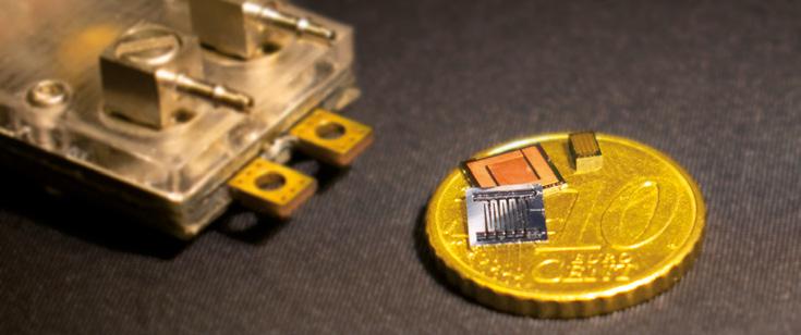
Researchers of the École Polytechnique Fédérale de Lausanne (EPFL) decided they can do better, for power electronics at least. By designing extensive plumbing into the chip, thus putting the coolant mere micrometers away from where heat is produced, the Swiss managed to increase cooling performance by a factor of 50.
Cold plate
Elison Matioli and colleagues at EPFL’s Insitute of Electrical Engineering demonstrated microfluidic cooling systems integrated into gallium nitride-on-silicon (GaN-on-Si) chips, which are anticipated as the next-generation power semiconductors. Wide-bandgap semiconductor GaN has excellent qualities for power applications, but it’s difficult and expensive to make (large) wafers out of the material. Hence the alternative approach to apply it as a thin layer on a silicon substrate. The silicon typically lacks functionality other than ‘carrying’ the GaN, but the Swiss researchers turned it into an active cooling layer by incorporating microfluidic channels into it – directly underneath the active transistor areas.
Using microfluidics to cool chips is, in itself, not a new idea. In one general approach, a microfluidically cooled ‘cold plate’ is stacked on top of the chip. The drawback of this approach is restricted heat flow. In another general approach, coolant is brought directly into contact with the die’s surface, which is much more efficient. Pumping coolant through parallel microchannels etched directly in the die offers great performance, for example, but requires high-powered pumping and generates thermo-mechanical stress because of the high temperature gradient that arises.
Big step
Embedding the microchannels into the chip itself is an attractive solution from a thermal management perspective, but such an approach would increase the complexity and cost of constructing the device. The EPFL researchers managed to simplify the process by combining two design steps into one: in what they call a monolithically integrated manifold microchannel (MMMC) system, the microchannels right underneath the heat sources are integrated and co-fabricated in a single die.

The MMMCs are fabricated in three steps. First, slits are etched into the GaNon-Si substrate. Next, an etching procedure is employed to widen the slits in the silicon, as well as to form sections of channels that connect to produce an interconnected channel system through which the coolant can flow. Finally, the channel openings at the surface are plugged with copper. The power integrated circuit can then be fabricated in the GaN top layer.
Working at Imec, Tiwei Wei, who wasn’t involved in the research, describes the results as “impressive.” Experiments in an ACDC current converter fitted with MMMC cooling “show that heat fluxes exceeding 1.7 kilowatts per square centimeter can be cooled using only 0.57 watts per square centimeter of pumping power. Moreover, the liquid-cooled device exhibits significantly higher conversion efficiency than does an analogous uncooled device, because degradation caused by self-heating is eliminated.”
Wei does point out that some aspects of the invention require further investigation, such as the stability of the modified GaN layer over time. Still, the Swiss research “is a big step towards low-cost, ultra-compact and energy-efficient cooling systems for power electronics,” he concludes.
Credit: EPFL
Establish cohesion among all the diff erent disciplines and departments


Rather than sending a few team members to a relevant training, IMS reached out to High Tech Institute to develop its customized in-company edition of the System Architecting training, allowing the company to bring in a broad and diverse group of its team. “From mechanical to electrical and software engineers to the sales team, the goal was to get everyone on the same page, thinking at a system level.”


Currently, the high-tech machine maker IMS is active in delivering machines used in the assembly process for the smart device and automotive sectors, in addition to next-generation headlights and sensors for cars.
ims-nl.com hightechinstitute.nl/systems


Maarten Buijs is roadmap and program consultant at Photondelta.

Government-directed innovation is not the answer
The Covid-19 pandemic appears to change who’s in the lead in setting the course of innovation. Innovation has been very much driven by the forces of the free market, which determine whether or not a new product or service will be profitable and thus provide a reward for the risk and investment of the innovator. For deep tech, the startup model is the dominant model for crossing the so-called valley of death, which all deep-tech innovations have to go through in order to find the right product/market combination. Going from concept and functional model to profitable product typically takes two decades, with course adjustments and significant investments from mostly private parties needed along the way.
A good example of such a journey is the introduction of microfluidic biosensors for so-called point-of-need testing of diseases and medical conditions. At the moment, I’m involved in setting up a roadmap for the introduction of such sensors based on integrated photonics at Photondelta. My earliest interaction with them was as a department head at the former Philips Research organization, the Natlab. There, at the end of the nineties, we set up several major projects based on our capabilities in and breakthrough ideas about materials and processing. Research projects into flexible or electrowetting displays, organic electronics, printable devices and wearable devices were started. Also, a project on microfluidic biosensors was initiated, with detection based on magnetic nanobeads.
When I left the Natlab to focus on R&D of electron microscopes, I lost sight of the biosensor project. Occasionally, I saw updates of the tortuous route that it had taken in finding the right applicational angle. Later, I learned that it was transferred to Philips Medical Systems, where further significant investments were
poured into the product development of these sensors. For strategic reasons, it was passed on to Siemens Healthineers, which I assume will bring the product to market in the not too distant future. This innovation route spanning two decades is characteristic for deep-tech innovation.
Now, it’s extremely poignant to realize that had cheap, fast, sensitive and specific point-of-need Covid-19 tests been available on a wide scale half a year ago, history would have taken a different turn. Millions of lives would have been saved, societal progress would not have been set back.
For many, this is a wake-up call to change the way innovation is driven. If governments would proactively have poured a fraction of the trillions of euros lost to the pandemic into development of among others diagnostic tests, the world would be in a much better place. Let’s learn that lesson and have governments take the lead in innovation, starting with that looming catastrophe of climate warming, people say. The examples from war time situations (eg the Manhattan project) and rich autocratic surveillance states appear to support this idea.
My own experience has taught me that putting government directly in charge is not the answer and is bound to lead to significant waste. History has given us enough examples for that, like nuclear fusion or manned space exploration. For societies to be prosperous, as well as equal and free, governments need to focus on creating the right circumstances, not be directive in innovation. Massive investment in science and technology of prevention of pandemics and climate warming is warranted. However, innovation based on the outcome of this must continue to be driven by the forces of the market, within the boundary conditions set by the government.
HOW TO PROMOTE TECH IN CHILDREN’S EDUCATION
Tech companies are facing the problem that educational systems focus on lots of skills, whereas STEAM (Science, Technology, Arts and Mathematics) often remain subsidiary. In the meantime, the tech industry is screaming for newly educated professionals. How to solve this?
Include tech in language education One approach to this problem has been successfully implemented by The Inventors. In their latest Summer School program, the assignment from the local government was to make sure children (4-12 yo) would improve their language skills: read, write, discuss, present. But how to keep them motivated during the summer holiday? The surprising answer was: tech!
Inventing is popular
It might not come as a surprise to you that children like inventors. To them, inventors are really smart people who become famous because of the magical stuff they create. And of course, the children are right. So if you make inventing the central theme in your educational project, children will even like the implicit language lessons. It’s only a small step from inventing to tech: building and presenting your own inventions is fun for almost every pupil.
650 new inventors this summer
Last summer in the city of Eindhoven, 650 children went to summer school to improve their Dutch language. Many of them were children from expats working in tech companies. Others were children from refugees and also children from Dutch-speaking families were there. One thing that connected them all was The Inventors program. And yes: their language skills improved. But what really connected them was the imagination of becoming real inventors when they grow up. In fact: this summer, they already became real inventors while presenting their creations on deuitvinders.com!
Support from tech companies
Many schools currently work on new programs to decrease the backlog in education as a result of the corona lockdown. The Inventors program is a perfect basis for schools to address this issue. All tech companies sharing this vision are invited to support the Inventors Foundation. It’s in their interest as well.
The Discovery Factory is there to inspire youngsters for a future in design and technology. Projects are supported by tech companies such as ASML, Brainport Industries, Daf Trucks, Frencken Europe, Hager, NTS Group, Philips, Stam en De Koning and VDL Group, and by Bits&Chips as the media partner.


