
30 minute read
Katherine Lasonde '23
BY KATHERINE LASONE '23
Advertisement
Cover Image: The utilization of Nitrogen-vacancy quantum defects for NMR experiments Image Source: Unsplash Abstract
This paper demonstrates the feasibility of room temperature nuclear magnetic resonance (NMR) experiments through an inexpensive, tabletop Nitrogen-vacancy (NV) center spectrometer. The spectrometer operates in a low magnetic and microwave field, ambient temperatures and requires only commercially available components. The state of an NV center can be read out using optically detected resonance measurements (ODMR). While other NMR experiments use electromagnets, this experimental setup utilizes a permanent magnet source to decrease the cost and portability of the set up. Additionally, the Quanta Image Sensor (QIS) is used to count individual photons from singular NV centers. NV center readout is best observed in experiments with low light and high contrast conditions, which is perfect for the QIS but difficult with many complementary metaloxide semiconductor (CMOS) and charge couple device (CCD) image sensors. Applications of NV center spectrometer sensing includes detection of single-neuron action potentials, single protein detection, and investigations of meteorites. Motivation
Transistors are small semiconductor devices used to amplify and control electrical signals. Typically, transistors are composed of adjacent electron-doped (N) and hole-doped (P) regions. By allowing current to flow from an N to a P region or a P to an N region, the output power can be controlled. Based on the applied voltage to the transistor, the signal can be completely stopped or greatly amplified. Transistors are the fundamental building blocks of all computer electronics.
For the past several decades, classical computers have continuously improved in speed and size per the projection of Moore's law – the hypothesis that the number of transistors in an integrated circuit doubles approximately every two years. However, the transistors within the computers are beginning to become so small that they are approaching the size of an atom. Classical computing architecture improvements are beginning to slow as issues such as current leakage and electron tunneling become increasingly impactful as transistor size decreases (Britannica, 2019). Thus, a new architecture regime is being explored: quantum
computers.
Quantum computers follow laws of quantum physics — rather than classical physics — to perform computations. While classical bits are physical entities represented by a zero or one, quantum bits, also known as “qubits,” are physical entities that can be in a superposition of the zero and one states until they collapse. (That is, fall out of a quantum state and lose all of the associated information). The ability to be in superposition means that the qubit is neither a zero nor a one, but a combination of probabilities that are either zero or one. Further, qubits are represented by vectors and matrices in a vector space, unlike classical bits, which exist in a list of numbers. Thus, programmers can apply matrix multiplication and other linear algebra operations to qubits without them losing their quantum mechanical properties.
Further, the state of qubits can be entangled. This means that the probability of a qubit being a zero or one is tied to the fates of other qubits in the system. By entangling the states of qubits within vector space, quantum computers can speed up the output of many algorithms, as computations are being increasingly run in parallel.
To exemplify the difference between classical and quantum computers, imagine a computer trying to solve a maze. A classical computer would go through every path of the maze sequentially to see if it was successful. However, a quantum computer would test every single pathway in a single step. In other words, the quantum computer can solve the maze in one try. Many of the challenging problems of today are characterized by a “mazelike” quality, especially simulation and optimization issues (Langione, 2020). Due to the tendency of qubits to superimpose and entangle, quantum computers can quickly simulate complex atomic and molecular phenomena (Nielsen 2011). Thus, quantum computers have the potential to significantly improve ‘molecularly-based’ issues such as global warming by simulating atomic structures which could lead to carbon neutral and negative technologies. However, according Langione (2020), the most promising technologies are the ones which adapt existing infrastructures rather than completely overwrite them. Making extreme nation-wide changes overnight is difficult, but adapting current techniques is much more feasible. Thus, the following quantum technologies increase the efficiency of current industry standards rather than replace them are prioritized.
The first quantum computing application in global warming is the reduction of carbon emissions due to the production of fertilizer. The leading method to produce fertilizer is through the Haber-Boch process, which fuses together nitrogen and hydrogen to make Ammonia. this process is extremely inefficient economically and environmentally — 3-5% of the world's natural gas is expended on fertilizer synthesis every single year (Langione 2020). Scientists know how to improve the efficiency of fertilizer production: simulate every molecular interaction in the electrostatic field of the catalyst nitrogenase. This simulation could be started today, but it wouldn't finish for 800,000 years. On a quantum computer, the simulation time would take a day (Langione 2021).
Additionally, quantum computers will catalyze the hydrogen production industry. Currently, hydrogen conversion processes to fuels are
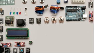
Image 1: Pictorial representation of transistors within all electronics.
Image Source: Unsplash
costly. Photovoltaic cells in solar cells may also increase 30-50% in efficiency with the help of quantum computing software (Langione 2020).
There are currently several competing climate change models that predict vastly different results. To create a climate model, many assumptions about the different interactions of regions throughout the globe are made. Characterizing those assumptions by leaving them as probabilities and creating one climate model could be an important driver for reducing global warming (Langione 2020).
Another key area that quantum computers will have an immense impact on is the infectious disease pharmaceutical industry. The design and analysis of molecules for drug development is a challenging problem today. From identifying the drivers of the disease, to screening millions of candidate activators and inhibitors, and developing a drug that can go to clinical trial testing is a process that takes typically ten or more years per drug (Langione 2020). In addition, 90% of those drugs fail to pass the clinical trials, costing companies billions of dollars.
Scientists already know how to design a drug based on searching through a massive chemical space to find the best fitting compound. However, building, tracing, and exactly describing and calculating all the quantum properties of all the atoms in a molecule is an extremely difficult computational task (Ghose 2018). Then, converting this information into chemical a database for searchable drug design would take 5 trillion, trillion, trillion, trillion years. This clearly not feasible. But, on a quantum computer, this process would only take 30 minutes. Since a quantum computer operates using the same quantum properties as the molecule it’s trying to simulate, future large-scale quantum simulations for drug development could treat everything from Ebola to HIV to Alzheimer’s (Ghose 2018).
Both hardware and software developments are required to turn these applications into reality. Challenges in quantum computing lay mainly in designing and controlling quantum hardware systems. Current quantum computing hardware is currently small-scale, because as the number of qubits in computation increases, there is a higher likelihood for error. Due to the atomic nature of qubits, their states are very fragile and susceptible to small effects. As the number of qubits in a system increases, the more likely one of the many qubits will ‘collapse’ (lose all its data). Qubits may collapse for a variety of reasons, such as random electron movement. The understanding of how to correct qubit errors, a field known as quantum — is still a largely emerging field.
Furthermore, quantum algorithms do not provide many, if any, advantages in reading or printing data compared to classical algorithms. Scientists have not yet figured out how to capitalize on quantum properties for reading and writing data (Biamonte 2017). Thus, the time it takes for a quantum algorithm to read or print data may prevent it from having a faster run time than its classical counterpart. Additionally, very little is known about the number of logic gates used in various quantum machine learning algorithms, so it can be hard to estimate their runtime. There has also not been extensive testing of the runtime of many quantum machine learning algorithms, so it is impossible to assert that they are superior to their classical counterparts.
Quantum states are incredibly fragile and are easily destroyed by temperature & pressure fluctuations, stray electromagnetic fields, and collisions from nearby particularly. Currently, qubits are still far from being 99.99% error proof & only a few qubits can be controlled together at a time. There must be large strides forward in the fabrication of high-quality qubits on a hardware level and self-imposed error correction on the software level (Ghose 2018). Many times, quantum computers also do not improve the run time or memory usage of a classical computer.
To build such a powerful quantum computer, researchers need to design qubits with lower error rates, longer coherence times, lower costs and non-cryogenic operating temperatures. Unlike many qubit designs, diamond lattice qubits operate under ambient conditions (Liu 2018). This alleviates the need for quantum computers to rely on complex cryogenic storage facilities, making building NV-center qubits more manageable. Additionally, NV-centers can be easily entangled using electromagnetic driving fields (Benjamin 2011). Since NV centers are also located within a tough diamond, they are less susceptible to noise than other designs.
Nitrogen vacancy center theory
Replacing two neighboring Carbon atoms in a diamond lattice with a nitrogen atom and a vacancy (or “hole”) creates a nitrogen-vacancy
(NV) center in the lattice. Nitrogen atoms have five electrons. In the NV, three of the electrons form covalent bonds with surrounding Carbons. The other two electrons near the vacancy will form a lone pair (Eichhorn 2019). The carbons around the vacancy each have a single electron where the covalent bond used to be. The center carbon oscillates between covalently bonding to the left and right carbon as shown in the diagram below (Haque 2017). This nitrogenvacancy pairing in a diamond is known as a ‘quantum defect,’ which is a physical entity that models a quantum-mechanical system.
The quantum defect has special electronic states within the band gap of diamond, allowing transitions between energy levels of the NV to be forced. NV center defects in diamond exist in three charge states: NV-, NV0 and NV+ (Eichhorn, 2019). In the NV0 state, the resonating Carbon bonding and lone pair on the nitrogen creates an ‘NV-axis’ line of symmetry, which induces three energy states in the defect. Inserting another electron (creating the NV- state), creates two pairs of unpaired electrons in the defect (Eichhorn, 2019). The NV0 state is paramagnetic (not magneto-optically active), while NV- state is not. Thus, the NV- charge state yields better results in high-resolution magnetic field sensing and imaging via optically detected magnetic resonance (ODMR) (Eichhorn, 2019). The NV- electronic states are thus used as opposed to NV0.
An NV- (NV) center in diamond has three main electronic levels: an excited triplet state, a metastable singlet state, and a ground triplet state. A singlet state (ms = 0 only) occurs when electron spins are paired in opposite (one up, one down) states and the energy levels of the electrons do not split when exposed to a magnetic field. A triplet state (ms = -1, 0, or 1) has three spin combinations – both up, both down, or one up and one down. The ms = 1 and ms = -1 states are degenerate, which means that the states have the same energy level (Haque, 2017). The combination of a magnetic field, microwave pulses, and 532 nm laser light are the main components required to create an NV center spectrometer in diamonds. Each component has a very specific and unique purpose, which will be detailed in the following paragraphs.
NV centers have an electronic spin property which can be manipulated by microwaves. Each electron in the NV center can either spin counterclockwise or clockwise, which corresponds to the +1/2 (spin up) and -1/2 (spin down) spin states (ms) respectively. A resonant magnetic field and microwave pulses across a frequency band of ~3.64 GHz. control the specific state that an NV center can be excited into from the ground energy state. The microwave pulses trigger polarization from the electron to surrounding carbon lattice, allowing manipulation of the electronic state.
Once NV centers are polarized, a green laser light (532 nm) can be shone into the NV center (Levine et al. 2019). This stimulates the unpaired electrons from the ground state (spin triplet) to the excited state (spin triplet) a higher energy state. The difference between the ground triplet state and the excited triplet state is referred to as the zero-phonon line. After a few milliseconds, the electrons will return to the ground state and release energy as series of 1.8 eV photons. (The color perceived as red by human eyes.) The variation in photoluminescent intensity is correlated to the resonance and spin to charge conversion (SCC) of the NV centers as manipulated by the green laser (Levine et al. 2019). Depending on the speed of the emitted photons and the microwave pulse sequence, an image sensor can determine the direction of the magnetic moment of the NV center.
Experimental goals and setup
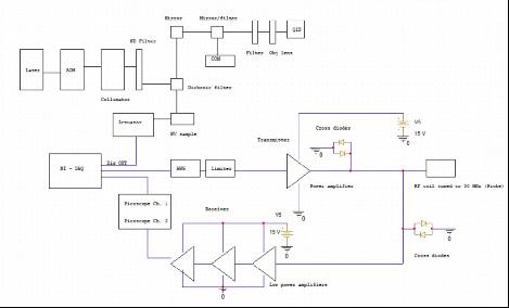
The general goal of the magnetic and microwave field setup of the experiment is to implement a sequence of pulses to induce excitation states in the NV centers through an antenna, DAQ, and a SPFT RF switch. There is also the creation of inhouse fabrication of a diamond sample holder & an NMR probe. Any commercial materials like the ones below may be swapped out. The overall schematic of this portion of the experiment is as follows:
Image 2: A nitrogen and vacancy pairing within a diamond lattice Image Source: Produced by Lasonde (author)
Image 3: Full experiment schematic
Image Source: Produced by Author
Image 4: Magnetic & microwave schematic. Note: To record ODMR spectra, a microwave field and magnetic field must be present. Image Source: Produced by Author
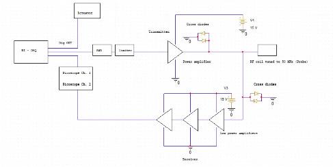
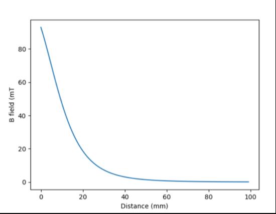
The general goal of this magnetic field is to create a 40 mT magnetic field needed for DNP experiments. This is implemented through a combination of a cylindrical Halbach permanent magnet array and a fringe field (about 1.2 cm from the Halbach magnet array). Placing a Halbach array of strength 170 mT approximately 12 mm away (on the coaxial z axis) from the sample will yield a proper magnetic field of approximately 40 mT.
Microwave Field
For this experiment, a microwave field will be generated at an approximate frequency of 2.87 GHz (±0.2). By broadcasting the microwaves from thin copper wires near the sample, ODMR spectra can then be determined by recording the change in fluorescence intensity as the microwave frequency changes. The microwaves excited a process of Landau-Zalner transistions that help to polarize the nuclei for the NMR.
Microwave Field: Description and Justification of the static setup
The base of the experiment was an optical table (board) which had mountable pieces to ensure accuracy of the setup. Custom linear actuator and Halbach magnetic mounts were designed and created. For our chosen actuator, an 8 cm by 8 cm by 1 cm aluminum rectangle was designed and manufactured to interface the optical mounting table and the manufacturer’s mounting bracket. Similarly, for our chosen Halbach ring, a 7 cm by 0.7 cm by 1 cm aluminum mount was designed and manufactured to mount the magnet to the optical table. The top portion of the mount has a half-cylinder groove cut such that only half of the Halbach ring sits inside the holder.
After the mounting and layout of the pieces was implemented, the design of the diamond sample holder must be considered. Design constraints considered include the size of the NMR probe and attachment to the linear actuator. The final design was determined to be a 5 mm wide by 30 mm long piece of ABS plastic. The diamond crystal is directly glued onto the holder. ABS plastic is transparent to microwaves and radio waves in the DNP and NMR experiments, and it will not interfere with the Halbach magnet.
Then, we pivot our attention to the programming of the linear actuator. The goal of the actuator in the experiment is to transfer the diamond sample approximately 14mm from the DNP setup (which includes microwaves) into the high magnetic field for readout such that the state of the NV center does not decohere, which means to fall out of a superposition or quantum state. (The collapsing of a qubit mentioned in the introduction). If the traverse speed of the actuator is 110 mm/s, it will take approximately take 0.13 seconds to move the sample 14 mm. Once in the magnetic field, the sample is coherent on the order of a few minutes.
The accompanying board to the L12-XXPT-3 Linear actuator required control parameters of min/max stroke length speed. To program these variables, the board interfaced with a TTL/PWM line connected to the computer through USB. The max stroke length was set to 30 mm and the minimum stroke length was set to 0.5mm. Furthermore, the goal of the actuator is to cover 14 mm in 0.13 seconds. Thus, the traverse speed of the actuator was determined to be 110 mm/s. Finally, the voltage of the actuator was set to 10V. However, the greater the voltage placed on the linear actuator, the faster the actuator will operate.
Microwave Field: Communications setup of the device
To program the sequential steps required of the experiment to occur at the proper times, a communications system must be built. The main two parts of the communication system include transmitting and receiving data.
The flow of data through the system is as follows:
1.The microwave sweep band is set to 3.54e4 GHz & the repetition rate is set to 147 Hz (manual)
2.The data acquisition device is turned on
3.NMR_setup.m is run
Image 6 (right): Magnetic field strength vs. distance from the Halbach Array (mm) Image 6 source: Produced by author
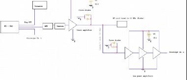
Image 7: T/R communications schematic
Image Source: Produced by Author
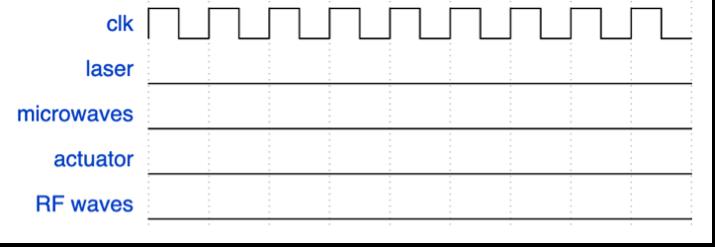
Image 7 (left middle): Timing diagram of the mw/rf/magnetics Image Source: Produced by Author
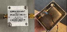
Image 8 (right middle): Picture of the limiter and the amplifier (with capacitors and cross diodes) Image Source: Produced by Author
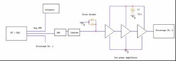
Image 9 (bottom): Transmitter schematic Image Source: Produced by Author 3a. Sets the RF signal and TTL signal HIGH
3b. Laser is turned on
4.Actuator is turned on moves the sample into the proper position
5.Data is then collected from the AWG and passed into the power amplifier to transmit the signal generated to the RF coil
6.The output of the probe is then passed to the receiver portion of the circuit, which consists of a limiter and a series of amplifiers
7.The output signal is then passed into the second channel of the picoscope
The diagram below summarizes the timing of events based on clock cycles: The schematic of the receiver communication system is shown in the diagram above. A signal from the AWG is passed into the limiter, which then is passed into three amplifiers and read out by a picoscope channel.
The purpose of the limiter in this design is to stabilize generator outputs, reduce amplitude variations, and protect low noise amplifiers and other devices power damage. Additionally, the purpose of each amplifier is to increase the size of the input signal. In experiments, input signals ranging from -70 dBm to -10 dBm will be passed into the system to be analyzed by the oscilloscope. Each amplifier has a pair of capacitors (470 uF and 220 nF ) to prevent noise from entering the system by bypassing it to the ground. Before the chain of amplifiers, there is a pair of cross diodes to ground that prevent power surges from ruining the circuit.
a. Laser
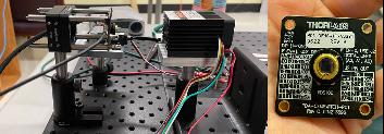
Light propagates through the system from a G150-1803 532 Nm Laser is a class IIIB laser system capable of a continuous power output ranging from 50 mW – 150 mw. This laser fires a continuous beam of green light to excite the spin +/- ½ electrons for the DNP experiment. NVs only need to be polarized once every T1e cycle, so a laser power in the order of mW is sufficient. However, the laser power must be better than 1% stable since ODMR is dependent on detecting relatively small (<10%) changes in the fluorescence intensity (Zhang et al. 2018). There are no requirements on the excitation wavelength, linewidth, or mode quality of the laser. Moreover, the laser is cw-mode and requires no synchronization or pulsing infrastructure for this experiment. The laser is controlled by a TTL line that will be hooked up to the Data Acquisition Device (DAQ).
The main difference between the pulsed vs. CW laser to consider is the sensitivity of fluctuations required for the experiment. With a pulsed laser, gated high-speed probing is possible, and the setup is less susceptible to certain types of noise. A CW laser is more limited in suppressing noise, and it requires a much more stable power supply (~10%). First, green photons from a 532 nm laser (I) are emitted into a fiber acousto-optic modulator (II). Then, a 100 MHz sound signal is used to attenuate the electrical signal in a manner such that the AOM will either permit light to pass through or be blocked. The light passed through the free space AOM propagates into a collimator, which is a “device for producing a parallel beam of rays or radiation” (OED). The collimator expands the beam width to allow for parallel optical and magnetic NV center detection. For now, the magnetic portion of the experiment will be ignored.
After the collimator has widened the beam, the laser light is passed through a neutral density (ND) filter to attenuate the power level to be a proper level for the CCD and QIS detection. The specified ND filter is composed of a UV fused silica glass substrate and a metallic Inconel coating through a full 270°. The data sheet guarantees a flat spectral response from UV to the mid-IR wavelengths.
b. ND Filter + Mirrors
The optical density is a linear function of the angle of the ND filter:
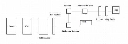
Image 10 (left): Antenna for the MW source
Image 11 (right): Optical subsystem schematic of the DNP/ NMR systems Image 10 & 11 sources: Produced by author
Image 12 (left): Optical subsystem schematic of the DNP/NMR systems Image source: Produced by author
Where OD is the optical density and theta is the angle in degrees. The value of m depends on the OD range of the filter, which in this case is 0-2.0. Thus, m = 0.00741. Furthermore, this formula assumes 0 degrees at the beginning of the coating & 270 degrees at the end of the coating.
The light is then manipulated using a series of filters and mirrors to allow the CCD and QIS to properly detect the surface and emissions properly. The first filter in the filter/mirror component subsection is a dichroic filter “used to selectively pass light of a small range of colors while reflecting other colors.” In this experiment, the laser emits green photons, but the NV center detection picks up on the red photon emission of the diamond. Thus, a dichroic filter which reflects green light but passes red light is required. Once light is passed through the dichroic filter, a mirror is used to alter the direction of light propagation from a position z direction to a positive x direction as specified to the axes above.
The beam is both reflected and passed through another mirror/filter into order to allow parallel detection of the surface and emissions via a CCD and QIS respectively. Finally, both the CCD and QIS has a specific filter & objective lens to prepare the light for proper detection.
c.CCD
The role of the CCD in the optical setup is to find the diamond’s surface. The CCD can detect white light coming off the diamond surface (and not necessarily emissions from NV centers). The light comes through the objective lens, such that the image of the surface can only be seen at the focal point. Thus, as the sample stage is manually moved toward the NV center, the image remains blurred until the lens reaches the target surface. The CCD is generally only used when a new diamond sample is mounted or when the sample-lens distance is much larger than the focal length. In this experiment, a commercial photodetector was used to detect the surface of NVs.
d.QIS
The QIS is a single-photon image sensor that measures light packets and generates binary measurements (Fossum, 2016). This allows the QIS to take pictures, or optically read-out, tiny cavities such as NV-centers without much noise. By decreasing the noise in the system, the QIS would immensely improve the scalability of NVcenter qubits.
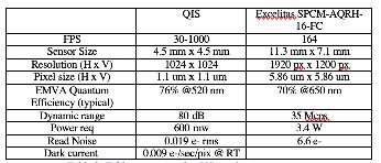
In the 2020 paper described by Misonou, a Basler based CCD camera was utilized due to the group’s previous experience with the device. The Basler ace camera, known as a 'workhorse camera,' is relatively cheap, flexible, high definition, and can run at 100 Hz or up to 3 kHz with a reduced ROI. This image sensor works well with a decent amount of light and is often paired with the QDM for readout. Any image sensors with reasonable specs can be swapped out for the Basler. A table of comparison of the QIS and the Basler ace is detailed in the table below:
In the experiment, signal red photons are imaged onto the single-mode fiber and collected by an SPCM, which in this case is the quanta image sensor. The key criteria of an effective SPCM for NV-center readout are high photon detection efficiency, low dark count, and high timing resolution.
Both the QIS and SPCM are photon detectors, and thus the two technologies can be interchanged. Typically, a CCD has a large field of view for imaging (or allows for wide spectral range when it's combined with monochromator), while an SPCM is more focused on high quantum efficiency and low dark counts.
The QIS model used in this experiment, nicknamed ‘Cupertino’, has a 16.7 Mpixel, 3D-stacked backside illumination with 1.1 μm-pitch pixels. The sensor can achieve 0.19 e- rms array read noise and 0.12 e- rms best single-pixel read noise under room temperature operation. The accurate photon-counting capability enables superior imaging performance under ultra-low-light conditions. The sensor supports programmable analog-to-digital convertor (ADC) resolution from 1-14 bits and video frame rates up to 40 fps with 4096×4096 resolution and 600 mW power consumption
The most important parameter to consider when swapping the QIS for the Excelitas SPCMAQRH-16-FC are the quantum efficiency in the 650-800 nm range. The SPCM used in the original experiment has the Q.E of 70% at 650 nm to 800 nm. The lower the QE of an SPCM, the longer it will take to collect photon counts and will compromise the sensitivity of the NV magnetometer. The dark count of the image sensor should also be below < 100 counts/s. The confocal capability of an image sensor is also crucial for single-NV detection.
The use of the QIS image sensor was determined to be the most beneficial for the experiment after a length analysis. As shown in the table above, the QIS has the smallest pixel size and lowest read noise and power consumption. The QIS can determine the number of photons more precisely than any other sensor, ensuring that a single photon is detected and not a whole stream of photons. NV ensemble regimes, which require low light conditions, pair well with CMOS image sensors. SPAD or scanning instruments are particularly effective with ensemble read-out due to their low photon count per pixel. However, most researchers currently have found a need for reading out one to an ensemble of ten defects at a time. Reading out ten individual NVs (one per pixel) is currently more complex than reading out an average of an ensemble of ten NV centers because of the high quantum efficiency and dark count required. In this regard, the QIS sensor is looking much better than the current SPAD technology (Turner). Since the QIS has particularly low read-out noise, single-photon light sensing applications, such as quantum interconnects, may benefit greatly.
In addition to NV centers, the QIS would help read out trapped ions, trapped cold atoms, and quantum dots as qubits (Turner). The QIS would also be great for scaling the number of photons or qubits read at once compared to SPADs. Since photon counting has historically not been available data, it is unclear exactly how this knowledge could benefit scientists; however, that doesn't mean the applications and benefits do not exist. In particular, the QIS will be particularly impactful in experiments with low-density samples, low light systems, noise-sensitive systems, and systems where the exact photon count is critical. The QIS is worth researching compared to current industry technology, particularly for the specific applications in which the QIS would excel.
Table 2: : Table comparing the QIS vs other image sensors Image Source: Produced by Lasonde (author)
Source: Produced by Author

e.Fiber optics
Finally, fiber optics were chosen to be used throughout the system. There are two main advantages of fiber optic cables. First, fiber optics make the laser alignment less susceptible to drift. Additionally, a fiber also acts as a spatial filter, such that putting a laser beam through a fiber cleans it up. The downside of using fiber optics is how long it takes to become accustomed to using them. Beginners typically take a few days to set up their first optical cable, but more advanced students may only take 20 minutes. Using a fiber instead of free space results in in higher strength, increased component reliability, and better production yields. Additionally, in free space, the beam diameter would have to be expanded from a couple millimeters to larger to meet the requirements of the image sensors through a beam expander.
Applications of a quantum sensing NMR/DNP
From this point forward, the entirety of the device built in this paper will be called a quantum diamond spectrometer (QDS). There are many advantages of using a NV center QDS than comparable technology on the market. First, the QDS has does not require narrowline width lasers for initialization and readout, meaning that a commercial green laser will work perfectly. Additionally, NV centers in diamond compute in ambient conditions (temperature & pressure), and thus do not require a cryogenic component as many other types of qubits do. Diamonds can be ethically grown, and the NV centers within them can also be ethically crated. They are naturally chemically inert, and thus are also biocompatible (Schloss, 2018).
There are many applications of the QDS in a range of fields for both ensemble and single NV center read outs. Ensemble readout is best observed in experiments with high photons levels and low contrast levels are best used in where ensembles are utilized. For example, quantum sensing of a field requires an ensemble of NVs to ensure a reasonable readout time (Hopper et al., 2018). On the other hand, single NV center readout is best observed in experiments with low light and high contrast conditions (which is excellent for the QIS either way) (Hopper et al., 2018). Diamonds with NV defects can be embedded within a living cell for magnetometry; electrometry; and thermometry conditions, potentially allowing for magnetometry in a single cell as well as electrometry and thermometry” (Abe, 2018). Recent biological examples of NV center sensing include ODMR detection of single-neuron action potentials, single protein detection, and NMR investigations of meteorite composition and paleomagnetism (Scholss, 2018).
Conclusion
Nuclear magnetic resonance (NMR) spectroscopy techniques are relatively insensitive compared other popular microscopy methods. H0wever, a spectrometer based on the fluorescent quantum defects in diamond, such as the colored NV centers in this paper, permit probing of sizes down to singular proteins and protons (Suter et al., 2017). The low sensitivity of magnetic resonance is an insurmountable barrier for technologies with biological application, and a quantum diamond spectrometer combined with NMR techniques may provide unprecedented information about molecular structure and dynamics. However, the present performance of quantum NV sensors remains far from their theoretical limits, and more work in the field is required (Schloss, 2018). Reading out the state of a single NV center requires low light and high contrast conditions (Hopper et al., 2018) is, for the first time, analyzed with the QIS. Fields dealing with microscopic organisms, such as biology, have low light conditions and need high contrast imaging.
Abe, E., & Sasaki, K. (2018). Tutorial: Magnetic resonance with nitrogen-vacancy centers in diamond—microwave engineering, materials science, and magnetometry. Journal of Applied Physics, 123(16), 161101. https://doi. org/10.1063/1.5011231
Biamonte, Jacob et al. 2017. “Quantum Machine Learning.” Nature 549(7671): 195–202.
Britannica, T. Editors of Encyclopaedia (2019, December 26). Moore’s law. Encyclopedia Britannica. https://www.britannica.com/ technology/Moores-law
Bucher, D. B., Aude Craik, D. P. L., Backlund, M. P., Turner, M. J., Ben Dor, O., Glenn, D. R., & Walsworth, R. L. (2019). Quantum diamond spectrometer for nanoscale NMR and ESR spectroscopy. Nature Protocols, 14(9), 2707–2747. https://doi.org/10.1038/s41596-019-0201-3
Deng, W. (n.d.). Deep Sub-Electron Read Noise in Image Sensors Using a Multi-Gate SourceFollower (invited). 6.
Eichhorn, T. R., McLellan, C. A., & Bleszynski Jayich, A. C. (2019). Optimizing the formation of depth-
confined nitrogen vacancy center spin ensembles in diamond for quantum sensing. Phys. Rev.
Materials, 3(11), 113802. https://doi. org/10.1103/PhysRevMaterials.3.113802
Fossum, E.R.; Ma, J.; Masoodian, S.; Anzagira, L.; Zizza, R. The Quanta Image Sensor: Every Photon
Counts. Sensors 2016, 16, 1260. https://doi. org/10.3390/s16081260
Ghose, S. (2018, Nov). A beginner's guide to quantum computing [Video]. TED Conferences. https://www.ted.com/talks/shohini_ ghose_a_beginner_s_guide_to_quantum_ computing?language=en
Haque, Ariful & Sumaiya, Sharaf. (2017). An Overview on the Formation and Processing of Nitrogen-
Vacancy Photonic Centers in Diamond by Ion Implantation. Journal of Manufacturing and Hopper, D., Shulevitz, H., & Bassett, L. (2018). Spin Readout Techniques of the NitrogenVacancy Center in
Diamond. Micromachines, 9(9), 437. https://doi. org/10.3390/mi9090437
Langione, M. (2020, Nov). The promise of quantum computers [Video]. TED Conferences. https://www.ted.com/talks/matt_langione_the_ promise_of_quantum_computers?language=en
Levine, E., Turner, M., Kehayias, P., Hart, C., Langellier, N., Trubko, R., Glenn, D., Fu, R. & Walsworth, R. (2019). Principles and techniques of the quantum diamond microscope. Nanophotonics, 8(11), 1945-1973. https://doi. org/10.1515/nanoph-2019-0209
Liu Gang-Qin, Pan Xin-Yu. Quantum information processing with nitrogen–vacancy centers in
diamond. Chinese Physics B, 2018, 27(2): 020304
Ma, J., & Chan, S. (n.d.). Review of Quanta Image Sensors for Ultra-Low-Light Imaging. 16.
Ma, J., Zhang, D., Elgendy, O. A., & Masoodian, S. (2021). A 0.19e- rms Read Noise 16.7Mpixel Stacked Quanta Image Sensor With 1.1 μmPitch Backside Illuminated Pixels. IEEE Electron Device Letters, 42(6), 891–894. https://doi. org/10.1109/LED.2021.3072842
Misonou, D., Sasaki, K., Ishizu, S., Monnai, Y., Itoh, K. M., & Abe, E. (2020). Construction and operation of a tabletop system for nanoscale magnetometry with single nitrogen-vacancy centers in diamond. AIP Advances, 10(2), 025206. https://doi.org/10.1063/1.5128716
Nielsen, M.A. & Chuang, I.L., 2011. Quantum Computation and Quantum Information: 10th Anniversary
Edition, Cambridge University Press.
Schloss, J. M. (2018). Optimizing NitrogenVacancy Diamond Magnetic Sensors and Imagers for Broadband Sensitivity. Physics Department, Massachusetts Institute of Technology. https://www.hertzfoundation.org/ wp-content/uploads/2020/10/Jenny-SchlossThesis-2019.pdf
Singh, M., Dhara, C., Kumar, A., Gill, S. S., & Uhlig, S. (2021). Quantum Artificial Intelligence for the
Science of Climate Change. arXiv [cs.AI]. Opgehaal van http://arxiv.org/abs/2108.10855
Suter, D., & Jelezko, F. (2017). Single-spin magnetic resonance in the nitrogen-vacancy center of diamond. Progress in Nuclear Magnetic Resonance Spectroscopy, 98–99, 50–62. https:// doi.org/10.1016/j.pnmrs.2016.12.001
Zhang, H., Belvin, C., Li, W., Wang, J., Wainwright, J., Berg, R., & Bridger, J. (2018). Little bits of diamond: Optically detected magnetic resonance of nitrogen-vacancy centers. American Journal of Physics, 86(3), 225–236. https://doi.org/10.1119/1.5023389


