


Separately, Integrate Seamlessly Using dsPIC33CH Dual-Core

dsPIC33CH dual-core DSCs are designed to facilitate independent code development for each core by separate design teams, which can subsequently be seamlessly integrated when the separate codes are later brought together. With the power of two dsPIC33C DSCs in a single chip, the dsPIC33CH family is optimized for several applications including safety-critical applications, touch control, wireless charging, digital power, motor control and many more.

performance with the power of two dsPIC33C DSCs in one chip
isolation of safety-critical frmware and real-time operation from rest of the application code
peripherals for
space and cost savings of up to 40% by eliminating the need for an additional microcontroller (MCU) and supporting circuits


time by
development by multiple teams
Metaverse is a new term that can be found in many presentations today And why not? Facebook turned Meta has burned some 20 billion dollars on Mark Zuckerberg´s grand idea Nokias CTO Nishant Batra predicted that virtual environment will replace our smart phones by 2030 Unfortunately I have to say: “Sorry guys, Metaverse will fail”.
But why? If you pour enough money into something, it will fly, right? This is not always the case. The Metaverse concept needs great hardware, excellent software and content that is needed and wanted in the market Meta ticks none of these boxes

Oculus Quest is a great device, but Meta needs to sell it in millions The beta users of Metaverse all complain about the experience saying it s like Fall Guys on the road. Facebook is not a great SW company. It has been hugely successful in developing algorithms for manipulation of user data, but the front end has always been clumsy User data needs to be totally secure and on this front the Facebook track record isn´t too glorious
Metaverse will, however, not fail on any of these shortcomings. It will fail, because there is not any single problem the concept will solve The pandemic got us all working at home and spend our time on endless video meetings, but that is not natural. When things get back to normal, we will want to meet face to face and interact Playing with avatars just will not be accepted
It is great that people have ideas. Not every idea is great though, regardless of financial resources
Editor in chief Veijo Ojanperä vo@etn.fi +358 407072530
Sales manager Anne Charlotte Lantz +46 734171099 ac@etn fi

Advertising prices: etn.fi/advertise
ETNdigi is a digital magazine specialised on IoT and embedded technology It is published 2 3 times a year.

ETN (www etn fi) is a 24/7 news service focusing on electronics, telecommunications, nanotechnology and emerging applications We publish in depth articles regularly, written by our cooperation companies and partners


ETN organises the only independent embedded conference in Finland every year The next Embedded Conference Finland is set for May 16 2023. More info on ECF23 can be found on the event website at www embeddedconference fi
The easiest way to access our daily news service is to subscribe to our daily newsletter at etn.fi/ tilaa
Veijo Ojanperä ETN, Editor in chiefCover photo: ROHM






If there is enough money, time and motivation, every system can be hacked. This is why embedded security is always a question of balance. How much do you want to invest in data security and what kind of risks are involved if someone breaks into your device? These questions were answered in the 4th annual Embedded Conference Finland in September.
Embedded security is notoriously poor in securing the devide, the connection and all data within But the SIM card and bank cards are sophisticated devices whose security has been fine for twenty years. Why cannot we secure other devices, asked application engineer Sigurd Hellesvik of Nordic Semiconductor in his ECF22 presentation
Even though data security has been fine for devices like the SIM card for a long time, the designers of many other devices make mistakes all the time A surveillance camera is a typical example of such a device
Fot the designer the problem is knowing what level of security is sufficient This is where standards, legislation and certifications come into play
Regulation varies widely Medical devices have very strict requirements, which is why it takes a long time, often years, to
other end of the line are consumer IoT devices Here the level of protection depends on the developer
The standards determine at least that the devices brought to the market meet the basic protection requirements, Hellesvik said But what about IoT standards? Luckily the European Union is already introducing stricter cyber security requirements in the next few years. For many these will come as a suprise, predicted sales manager Antti Tolvanen of Etteplan

NIS2 (Network and Information System Directive 2) directive was practically agreed upon in the summer Parliament voted on the content of the directive in late October and the new law will probably be published in early 2023
include NIS2 in their own legislation within 21 months, Tolvanen clarifies
NIS2 stipulates that all actors NIS2 speaks of essential and important "entities" must meet the new requirements The regulations apply to practically all devices connected to the network that use some kind of software to process digital data That means basicly every devices designed by an embedded designs, Tolvanen pointed out
Article 18 of the NIS2 directive says for example, that all operators must meet information systems security management specifications (ISMS), as well as strict equipment development and maintenance requirements This applies not only to equipment manufacturers, but also to their subcontractors
Regarding embedded devices NIS2 will

medical devices, computers, electrical components, machines and devices, engines and vehicles and other devices The regulations also apply to suppliers of managed information security services That is, if you maintain the client's software, you are an essential actor from NIS2's point of view, Tolvanen said

The big change resulting from the new EU legislation is that it makes CE markings obsolete.
For example, the regulations concerning most radio equipment (RED, radio equipment directive) were approved in January 2022 and they need to be applied in the beginning of August 2024 The problem is that the standard is not ready yet, and the equipment manufacturer probably does not have enough time to redesign the equipment so that they meet the new requirements
The new RED directive on radio equipment is quite strict For example, it says that the radio device must not disturb the network or abuse the network's resources in such a way that the quality of the connection and service suffers This should make it more difficult to use devices for, for example, denial of service attacks In addition, the devices must include mechanisms that protect the user's private data
This will create problems for manufacturers Before the harmonized standard is ready, bringing a product to the EU market requires approval by an authorized organization If the radio device has not been approved in accordance with the standard, it will become illegal at the beginning of August 2024 Even if the product is already on the market, it can no longer be sold if it
This can have surprising practical consequences Most of the routers sold in the EU are manufactured in China and at some point it will become a problem to get wireless routers to European market, Tolvanen predicted
The new EU legislation does not mean protectionism The task of the new legislation is to ensure that we can use safe devices in infrastructure in Europe With better security, it will become more expensive to engage in cyber attacks, he concluded

Infineon Technologies has announced commercial availability of the industry’s highest density serial F RAM. The new 8 and 16 Mbit EXCELON F RAM memories address the non volatile data logging requirements of next generation automotive and industrial systems to help prevent data loss in harsh operating environments The new memories feature a wide voltage operation from 1 71 V to 3 6 V and support up to 54 MBps of data throughput > etn.fi/14181
Onsemi has introduced its new ecoSpin family of brushless DC (BLDC) motor controllers By combining the control and driver functions in a complete system in package (SiP) solution onsemi simplifies the development of high voltage motor control systems in applications such as HVAC, refrigeration and robotics The first member of the ecoSpin
Ride Vision have introduces “ADAS for
The solution
and
capture high
them
of
and
the
Oracle has introduced a new version of Java The Java 19 JDK includes seven JDK enhancement proposals to increase developer productivity, improve the language, and improve platform performance, stability, and security However, most java coders use earlier versions

Java is one of the most popular
programming languages In various comparisons, it always ranks at the top There are 60 billion java virtual machines in the world
The last time the versions used by java coders were studied at the beginning of the year, at that time it turned out that the most popular java version is Java 11, which was announced in September 2018. It
At the 2022 IEEE International Ultrasonics Symposium, imec research center presented a piezoelectric Micromachined Ultrasound Transducer (pMUT) array that is compatible with flat panel displays (FPD) process technologies The array demonstrates acoustic pressures in mid air above 1kPa, a pressure level relevant for enabling mid air haptics and directed sound Moving from wafer based to FPD compatible processes prepares the pMUT technology for the integration of future mid air applications, such as vibro haptics, time of flight (3D) sensing or gesture recognition, in
novel form factors like smartphones and car dashboards This technology can be used to create touchless, interactive, screens in automotive and consumer applications, or used in gaming
Ultrasound technology can be used to equip smart systems with haptic feedback, giving the user a sense of touch In the case of mid air haptics, ultrasonic waves produce a local pressure field causing the user to ‘feel’ a light sensation without touching the object Such applications require high pressures at low ultrasonic frequencies Current solutions include, on the
was used by 48 percent of developers Java 8, introduced in March 2014, was trusted by 46 percent

Whether the introduction of new versions is slow or not, Oracle brought new features this time as well In Java, these are called JEP (Java Enhancement Project). For example, new features come from the OpenJDK project Amber (Record Patterns and Pattern Matching
JEP 424 is again known by the project name Panama, and it develops technology with which Java programs communicate outside virtual machines with native libraries and data. JEP 422 tries to make java virtual machines run on RISC V based devices.
one hand, large standard piezoelectric elements that produce relatively high frequencies impeding a precise interaction with the user On the other hand, small silicon based micromachined transducer arrays can enable haptic feedback at short distance in a small area only
Imec’s FPD compatible thin film pMUT array now fills the niche for low frequency, high pressure devices for large volume mid air applications Peak pressures of 1 5 kPa in air at resonant frequencies in the range of 200 to 400 kHz have been demonstrated replicating the performance metrics needed for mid air haptic feedback
Oracle delivers new Java Feature releases every six months according to a predictable release schedule This cadence provides a steady stream of innovation while continuously improving platform performance, stability, and security, helping to increase Java adoption in organizations of all sizes and industries
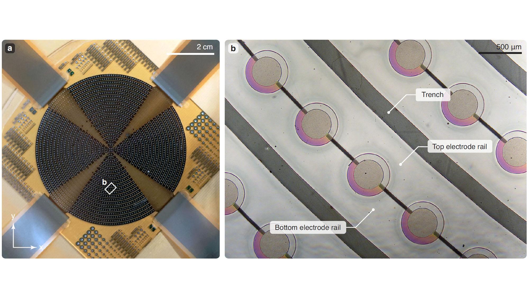
(A) A large area pMUT array consisting of 22 phased annular rings of 500 µm diameter pMUTs (B) Detail. With pMUT arrays it is possible to implement gesture recognition and ToF sensing into different size displays. This pays way to new user interfaces in many applications.
An international group of researchers from Technical University of Denmark (DTU) and Chalmers University of Technology in Gothenburg, Sweden have achieved dizzying data transmission speeds and are the first in the world to transmit more than 1 petabit per second (Pbit/s) using only a single laser and a single optical chip

Researchers succeeded in transmitting 1 8 Pbit/s, which corresponds to twice the total global Internet traffic And only carried by the light from one optical source The light source is a custom designed optical chip, which can use the light from a single infrared laser to create a rainbow spectrum of many colours, i e many frequencies Thus, the one frequency (colour) of a single laser can be multiplied into hundreds of frequencies (colours) in a single chip
All the colours are fixed at a specific frequency distance from each other just like the teeth on a comb which is why the device is called a frequency comb Each colour (or frequency) can then be isolated and used to imprint data The frequencies can then be reassembled and sent over an optical fibre, thus transmitting data Even a huge volume of data, as the researchers have discovered
The experimental demonstration showed that a single chip could easily carry 1 8 Pbit/s, which with contemporary state of the art commercial equipment would otherwise require more than 1,000 lasers The researchers also created a computational model to examine theoretically the fundamental potential of the technology The calculations showed enormous potential for scaling up the solution
Navitas Semiconductor has taken the power semiconductor market by storm and will showcase industry leading gallium nitride (GaN) and silicon carbide (SiC) technologies at Electronica 2022

The company will have several new products on show Like the new 650 V, MHz GaNSense gallium nitride half bridge power ICs, which provides autonomous, loss less sensing and 6x faster protection Another new device family is the 750 V 6 5 kV GeneSiC silicon carbide power MOSFETs with
Navitas is best known for its fast charging chips for mobile devices In Munich the company will show mobile fast chargers up to 200W with 0 100% charge in less than 10 minutes
GaNFast power ICs integrate gallium nitride power and drive, with control, sensing and protection to enable up to 3x faster charging, 3x higher power density, up to 40% greater energy savings in half the size and weight of legacy silicon chips in half the size and weight of legacy silicon chips


Researchers from IDLab (an imec research group at Ghent University and the University of Antwerp, Belgium) and Nokia Bell Labs have presented the first upstream linear burst mode transimpedance amplifier (TIA) chip that accommodates 50 Gbit/s NRZ and 100 Gbit/s PAM 4 modulation The chip enables optical line terminals (OLTs) to cope with upstream packets’ varying signal strength and quality degradation
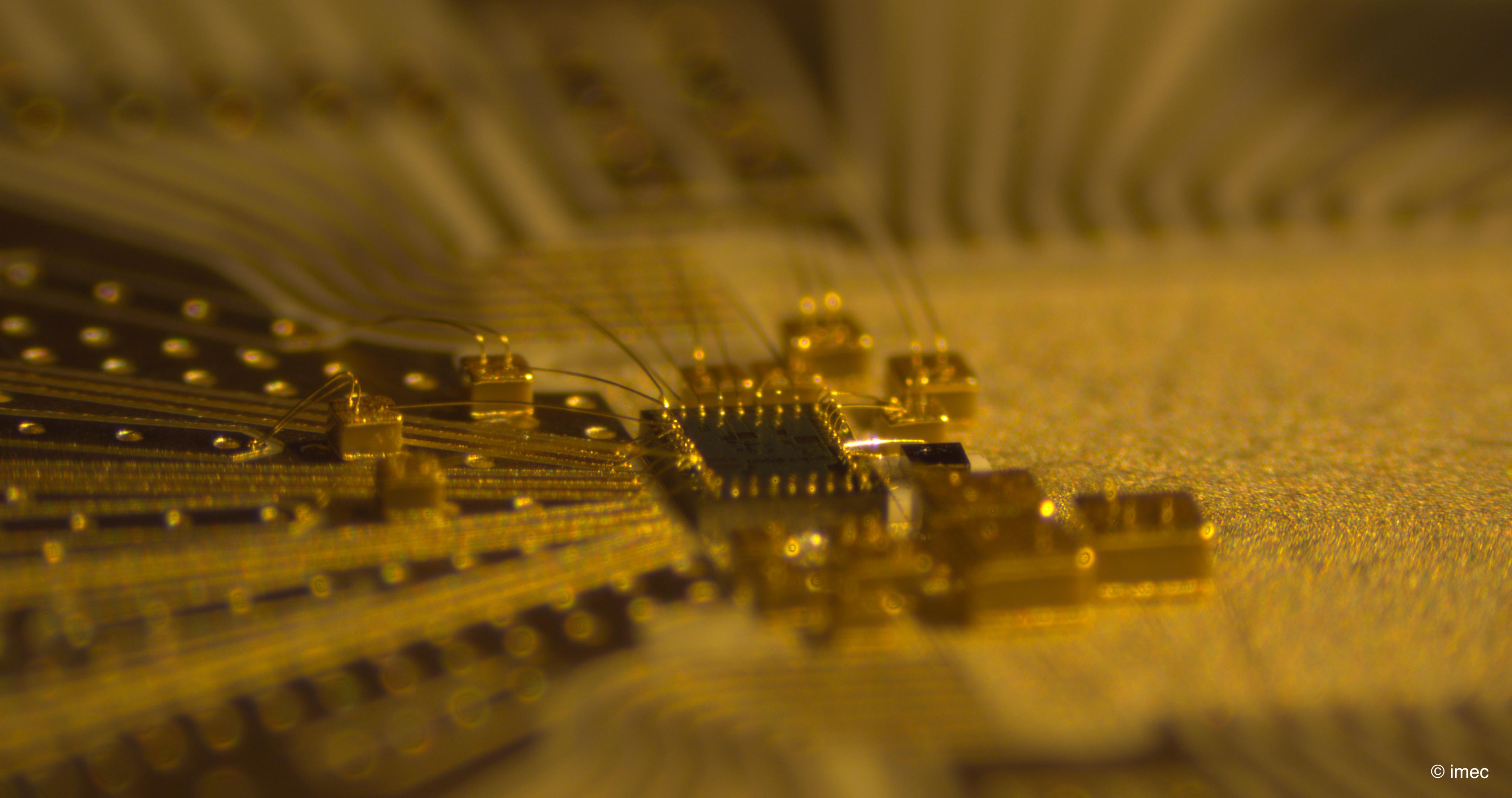
This novel TIA chip will be critical to making next gen flexible PON deployments (and 100G PON networks in particular) technically and economically viable.
Passive optical network (PON) technology brings high speed broadband to residential and business subscribers, while
PON networks are characterized by a tree like network topology that allows to serve multiple customers with a common strand of fiber connected to a single optical line terminal (OLT) in the operator’s central office. This makes for a cost effective deployment scenario, but it also impacts how packets travel the network: downstream traffic is sent over the network continuously, while upstream traffic is transmitted in bursts (within allocated time slots, preventing collisions).
The TIA chip was introduces at European Conference on Optical Communication (ECOC) which was organised in Basel of Switzerland at the end of September
Pulsiv OSMIUM uses a patented method for converting AC to DC that involves charging/discharging a small storage capacitor without the need for a PFC inductor This unique solution delivers high power factor, consistently high efficiency and an ultra compact system design. Pulsiv OSMIUM technology can be used to improve overall system
efficiency, optimize cost and contribute towards reducing global energy consumption

The Pulsiv OSMIUM microcontroller family and supporting components can be combined with commodity flyback DC DC converters to displace higher cost LLC solutions Pulsiv has
demonstrated a universal input, single switch 150W flyback power supply design that delivers 97 5% average (99 5% peak) front end efficiency while maintaining 90% at just 2W A 240W interleaved flyback is currently being developed and work is underway to showcase reference designs with even higher power capability.
Microchip Technology has introduced a new family of META DX2+ PHYs These are the industry’s first solution set to integrate 1 6T (terabits per second) of line rate end to end encryption and port aggregation to maintain the most compact footprint in the transition to 112G PAM4 connectivity for enterprise Ethernet switches, security appliances, cloud interconnect routers and optical transport systems
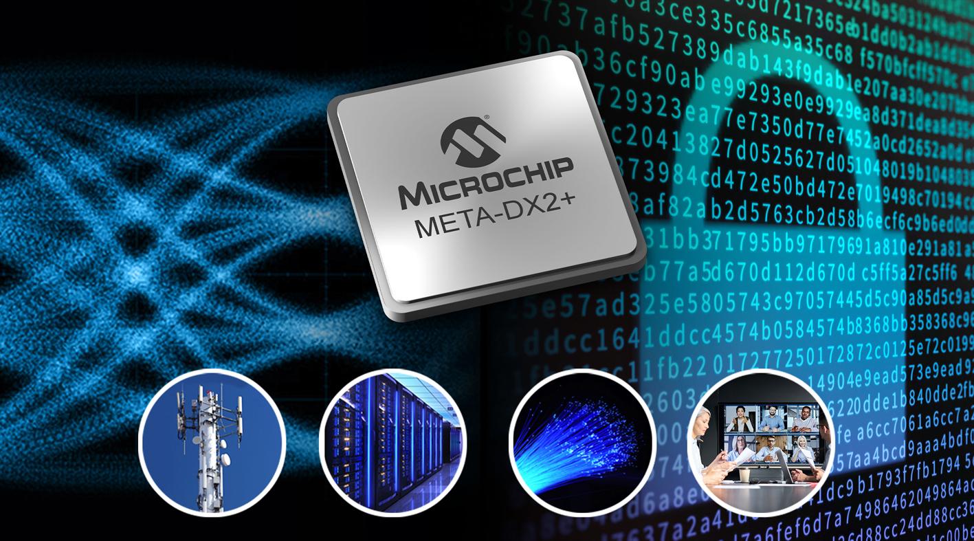
The META DX2+’s configurable 1 6T datapath architecture outperforms the next near competitors by 2x in total gearbox capacity and hitless 2:1 protection switch mux modes enabled by its unique ShiftIO capability The flexible XpandIO port aggregation capabilities optimize router/switch port utilization when supporting
Pulsiv OSMIUM microcontrollers (PSV AD 150 and PSV AD 250 sampling now) do not directly determine output power and can be used as a platform for any application requiring 1W to 10kW, by adjusting only three system components and connecting a suitable DC/DC converter
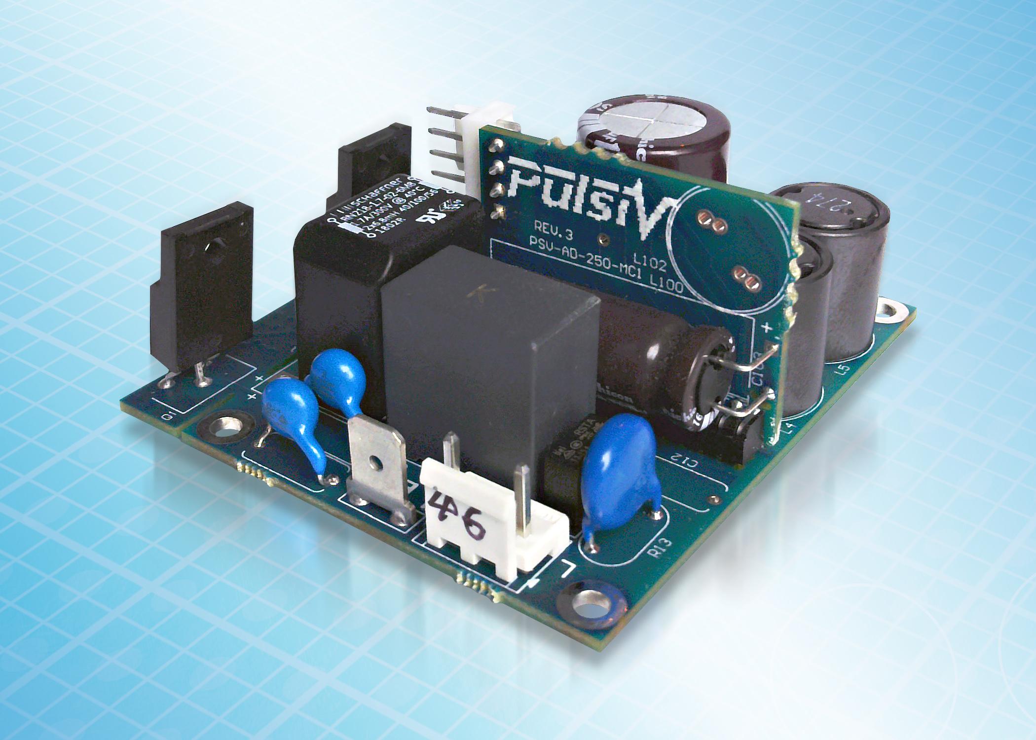
Critical components in a Pulsiv OSMIUM circuit operate at low
low rate traffic Also, the devices include IEEE® 1588 Class C/D Precision Time Protocol (PTP) support for accurate nanosecond timestamping required for 5G and enterprise business critical services By offering a portfolio of footprint compatible retimer and advanced PHYs with encryption options, Microchip enables developers to expand their designs to add MACsec and IPsec based on a common board design and Software Development Kit (SDK)
Like the META DX2L retimer, the new series of META DX2+ PHYs can be used with Microchip’s PolarFire® FPGAs, the ZL30632 high performance PLL, oscillators, voltage regulators, and other components that have been pre validated as a system to help speed designs into production
In January, the European Union decided that from the beginning of 2024, the USB type C connection will be a mandatory charging connection for a large number of battery powered portable devices Now the commission has finally approved the charger standard This means that Apple will have to switch to USB C in iPhones > etn.fi/14160
The 2022 Millennium Technology Prize has been awarded to Scientia Professor Martin Green of the UNSW Sydney, Australia, for his leadership in the development of the Passivated Emitter and Rear Cell (PERC). Since its development in 1983, the PERC has gone on to become the most commercially viable and efficient silicon solar cell technology for use in solar panels and for large scale electricity production, accounting for almost 90% of the global solar cell market > etn.fi/14159
TouchNetix’ family of aXiom touchscreen user interface chips are made for the next generation vehicle cockpits as the automotive industry increases its focus on more intuitive and enhanced user experiences The latest addition to the aXiom product family is the AX198A supporting ultra wide touchscreens up to 65” LCD and OLED display technologies in a single chip The chip is automotive qualified > etn fi/14147
temperatures to extend their expected operating life, even under convection cooling
The BMI323 by Bosch Sensortech is a general purpose, low power IMU that combines precise acceleration and angular rate (gyroscopic) measurement with intelligent features that are triggered by motion Its integrated features make development faster and easier The sensor includes Bosch Sensortec’s plug and play step counter software, so customers don’t need to spend time developing their own algorithms etn.fi/14143
Intel has demonstrated an early prototype of next generation Thunderbolt in action, aligned to the USB Implementers Forum’s (USB IF) release of the USB4 v2 specification in September Next generation Thunderbolt will deliver 80 gigabits per second (Gbps) of bi directional bandwidth and enable up to 120 Gbps for the best display experience, providing up to three times the capability of today’s technologies
As before, the new spec will maintain compatibility with previous versions of Thunderbolt and USB. According to Intel Thunderbolt 5 will hit the market in 2023
The prototype demonstration marks a major milestone in the journey to delivering next generation Thunderbolt to the industry The bandwidth needs of content creators and gamers are increasing significantly for high resolution displays, low latency visuals, and the backup or transfer of huge video and data files Next generation Thunderbolt will deliver up to three times the capability of Thunderbolt 4 and make creating and gaming more efficient and
immersive The next generation of Thunderbolt will include improvements across a variety of areas including:
• Two times the total bandwidth of Thunderbolt 4 to 80 Gbps, while providing up to three times the bandwidth to 120 Gbps for video intensive usages.
• Support for the newly released DisplayPort 2 1 for the best display experience

• Two times the PCI Express data throughput for faster storage and external graphics
• Works with existing passive cables up to 1m via a new signaling technology
• Compatible with previous versions of Thunderbolt, USB and DisplayPort
• Supported by Intel’s enabling and certification programs

In 2019 Intel contributed to the USB Promoter Group its Thunderbolt protocol specification, which served as the basis for USB4


U blox has announced new explorer kits to make it quicker and easier for engineers to design and evaluate products requiring centimeter level positioning capabilities
Set to launch in early 2023, the ready to use XPLR HPG 1 (pictured right) and XPLR HPG 2 solutions will for the first time combine u blox’s unique offering across the key technologies required to achieve highly precise positioning As well as an open MCU, they’ll include high precision GNSS (HPG) positioning with real time kinematic (RTK), dead reckoning, cellular, Wi Fi and Bluetooth communications, and the necessary antennas The kits are designed to integrate seamlessly with complementary u blox services, such as PointPerfect
GNSS augmentation service, and the ubxlib software component Ubxlib simplifies the developer experience across u blox products and services, particularly during component evaluation and prototyping
he kits will assist engineers orking in areas such as micromobility and low speed obotics, helping them build, est and demonstrate early tage proofs of concept more quickly, thereby upporting faster overall me to market
Both kits will include the full gamut of u blox technology and software required The modular XPLR HPG 1 kit will be based around the wireless MCU in the u blox NORA W106, with its Wi Fi and Bluetooth LE capabilities, and will give engineers flexibility to adjust their
The Connectivity Standards Alliance, the international community of more than 550 technology companies committed to open standards for the Internet of Things, have announced the release of the Matter 1 0 specification and the opening of the Matter certification program.


A long time in the making, Matter 1 0 is meant to control all smart devices at home, regardsless the radio technology they use for connection
It s a bold idea, but how does it work in practice. Skip Ashton of Infineon and a member of the Board of Directors of the CSA, expaines
The Matter Software Development Kit (SDK) has an application code for the device types supported by Matter. So you can build a door lock, or a light bulb by configuring the SDK for your specific application Of course, the Matter SDK does not know how you control your light bulb, so if a message comes in “Dim light to 50%” the SDK will check if the message is correct,
Matter protocol will all have different functions and settings. How will these be handled?
Each device has mandatory and optional functionality When a Matter controller discovers a new device it can query it to see its functions and then adapt its controls accordingly, says Ashton
solutions to their precise needs, using MIKROE Click boards The kit will include three Click boards, which respectively incorporate the ZED F9R high precision RTK GNSS module, the LARA R6001D LTE Cat 1 module (global coverage and with built in MQTT client), and the NEO D9S L band correction data receiver module Engineers can purchase others, based on their application’s needs The kit’s source code will include example software for the Espressif IoT Development Framework (ESP IDF), based on ubxlib software components
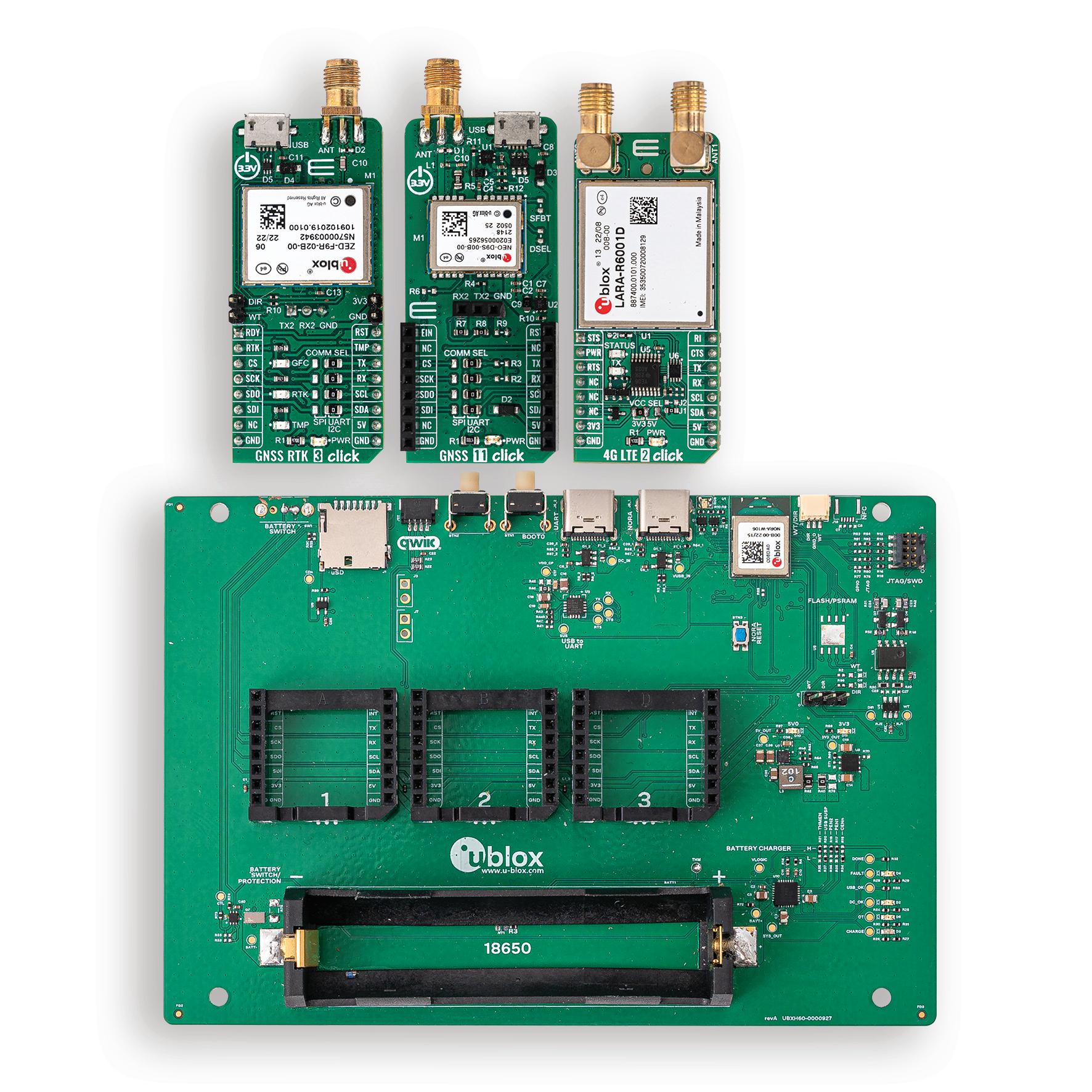
The compact XPLR HPG 2, meanwhile, will incorporate the ZED F9R high precision RTK GNSS, LARA R6001D LTE Cat 1 (with global coverage and built in MQTT client) and NEO D9S L band correction data receiver modules, as well as the NINA W106 with its MCU, Bluetooth LE and Wi Fi capabilities
source reference design software development kit (SDK) is complete all to bring new, innovative products to market Further, Alliance members with devices already deployed and with plans to update their products to support Matter can now do so, once their products are certified
New four year EU funded Horizon Europe project ROADVIEW strengthens European competence in automated driving, by concentrating on one of the biggest challenges in the field: operating efficiently in different weather and traffic scenarios. Specialised in all weather SAE Level 4 full stack software for automated vehicles, Sensible 4 is one of the partners in the consortium.
Sensible 4, a Finnish automated driving technology company, is one of the 16 partners in the new EU funded project Robust Automated Driving in Extreme Weather (ROADVIEW), which aims at developing more robust and cost efficient in vehicle perception and decision making systems for connected and automated vehicles Sensible 4 supports the whole consortium with the standardisation roadmap, strategic partnerships, and future exploitation of project results The project has a total budget of 10 million euros and focuses on enhancing the performance of autonomous vehicles under harsh weather conditions and different traffic scenarios

This project strengthens our existing competence in all weather
driving and it is closely aligned to our product roadmap for the next four years. It will enable further improvements to our technology and provide new opportunities to test it across different sites, together with a highly innovative consortium of research and industrial partners, says José Camposano, project manager, Sensible 4.
ROADVIEW started at the beginning of September and will continue for the next four years For Sensible 4, this period will focus on expanding the capabilities of its automated driving system and providing additional support, to enable safe and efficient performance in more challenging Operational Design Domains
Some of the innovations in the project are the integration of SAE Level 4 software modules across different vehicle platforms, as well as the use of state of the art tools for X in the loop simulation and testing The new software components developed during this project by Sensible 4 will be demonstrated in different vehicles and outdoor environments, including Finnish Lapland More info here: ROADVIEW
The University of Oulu strengthens the training of cyber security experts The training will focus on the technical competence needed to ensure cyber security In practice, training will be offered to students from next spring as an area of specialisation in the Master's degree programme in information technology at the Faculty of Information Technology and Electrical Engineering > etn.fi/14108
GaN Systems from Ottawa announced that the new Renesas Electronics´ automotive 48V/12V Bidirectional DC/DC Converter is powered by GaN Systems power transistors, resulting in significant power density improvements. The new converter uses GaN Systems’ GS61008P, a 100V enhancement mode GaN on silicon power transistor, to achieve a 46% reduction in system size > etn.fi/14107
Nokia will lead the Hexa X II project, the second phase of the European 6G flagship initiative This new phase will expand the Hexa X partner list to 44 organizations that are tasked with creating the pre standardized platform and system view that will form the basis for many inputs into future 6G standardization The Hexa X II project aims to start work on 1 January 2023 > etn fi/14095
Aeries II by California based Aeva is the world's first 4D light radar It senses the movements of objects in three dimensions and their speed accurately This becomes the fourth dimension of the lidar Aeva's lidar is based on FMCW (Frequency Modulated Continuous Wave) technology It is a continuously radiating transmitter whose frequency can be changed during the measurement Accurate measurement of speed is possible only by utilizing such a phase difference > etn fi/14088
15-18 November, Munich, Germany
C4, Booth 125
Breakthroughs in collecting and connecting patient data are key to helping improve outcomes. But diagnostics can’t help if you can’t trust the data. ADI’s iCoupler digital isolation technology is instrumental in protecting patient data, and the patients themselves, as we continue to explore the frontiers of modern medicine.
Analog Devices. Where what if becomes what is. See What If: analog.com/WhatIf






Robots are becoming ever more prominent, helping us carry out tasks that we humans think of as dull, dangerous, or dirty. Robot vacuum cleaners help us clean the house, robotic lawnmowers keep our grass neat and tidy. Likewise, driving assistance has developed rapidly and automated vehicles are more frequently visible on the streets - albeit with a safety operator
As for driving from Helsinki to Rovaniemi fully autonomously without any human assistance (also known as SAE Level 5), I believe this will not happen for a long time Since the beginning, Sensible 4 has believed in the advantages of SAE Level 4: automated driving without a driver but with remote operations that can assist fleets of vehicles Many other companies have also realised the difficulty of Level 5 and pivoted their strategy to focus on Level 4 which can already take us far
To reach the point where we have Level 4 automated vehicles, without a safety operator onboard, requires more than just technological development Legislation and regulations must be developed further as well as solutions to “unpredictable road users”; pedestrians, cyclists, and human drivers

Fundamentally, there has to be a clear business case where automated driving provides a solution to a real life problem Automated vehicles can speed up electric vehicle usage, they are fuel efficient and provide a solution for the growing shortage of drivers that many
countries face In Europe, there is a 20% shortage of truck drivers New technology is often expensive and automated vehicles, with a safety operator onboard, are not commercially viable Instead of trying to solve all the challenges at once, companies tend to target niche use cases or segments, where the business can become commercially viable in a shorter time frame
Sensible 4’s automated driving software platform DAWN enables different types of vehicles (trucks, vans, shuttle buses) to operate autonomously in any weather Our technology is developed in the four seasons of Finland, and we have carried out multiple successful automated driving projects, on public roads, around the world


We are now taking the product to the industrial segment where the closed environment makes it readily commercially viable A closed operation is not without its challenges, but we are successfully operating a heavy duty truck year round autonomously in an industrial environment that is dusty, muddy, and sandy


From the closed area, the logical next step is to public roads without passengers In a couple of years, we believe, that DAWN carries passengers
with last mile shuttles on public streets That is our plan Maybe someday, there will be enough niche focused technologies that combine into a Level 5 automated vehicle Then again, Level 5 automation is described as the most complicated technical engineering challenge to mankind We might eventually get there, but it requires huge technological leaps While waiting, let’s enjoy the smaller steps they already make our everyday lives easier
arri Santamala is the EO and co founder the Finnish self iving technology


ompany Sensible 4 antamala is one of e pioneers behind e Finnish road utomation
cosystem and was one of the first ones to take automated buses to open road conditions in 2016 At Sensible 4, Santamala’s work focuses on developing new technologies to the autonomous driving space that will speed up the (highly anticipated and needed) shift from fossil fuel based transportation to a more sustainable model of shared driverless mobility
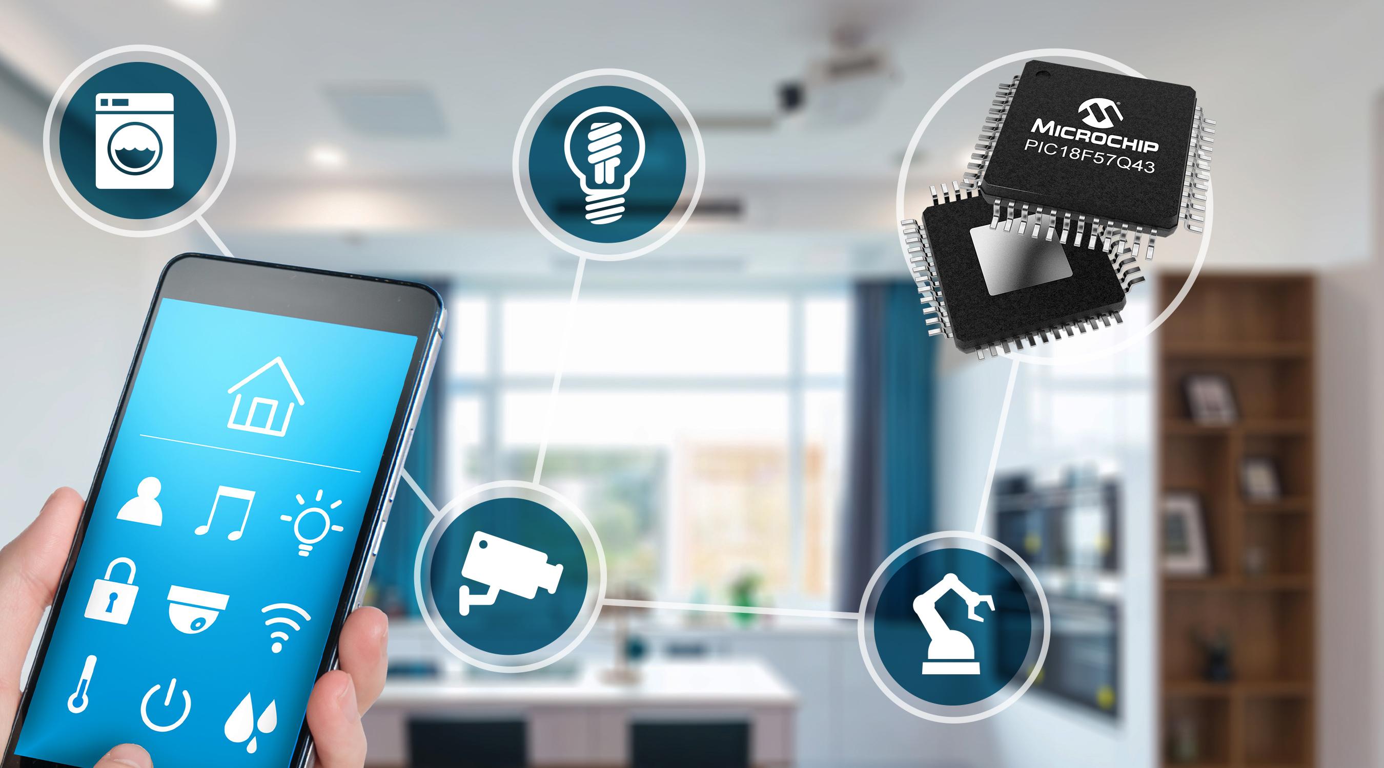
8 and 16 bit MCUs are an invaluable tool for performing small, specialized tasks. The tasks aren’t necessarily complex, but they can be time consuming or time critical. By offloading the tasks, the 32 bit devices can have simpler implementations that improve reliability, reduce memory usage, and lower power consumption.
In today’s world, large 32 bit microcontrollers and microprocessors running a real time operation system (RTOS) are increasingly common. However, a single large microcontroller handling a complex application may run into issues with CPU resources with
regards to small housekeeping tasks, which are not complex, but are time consuming

Smaller devices, like 8 and 16 bit MCUs, can be used to offload these tasks from the 32 bit device. Consider the following example: a 32-bit MCU is used to
control the non safety features of a car, like the entertainment system, ambient lighting, and the A/C The 32 bit device must allocate its resources to process all of the tasks associated with these features A few examples include measuring the temperature of the cabin in multiple points, turning on/off the A/C systems, updating the graphical display, processing user inputs, adjusting lighting conditions, and playing music
Even for a large 32-bit device, this is a lot of work
However, these tasks are more manageable if the 32-bit device
offloads some of these tasks to sub processors that handle only 1 or 2 of these tasks but require little supervision in doing so This frees up CPU resources on the main processor, which reduces software complexity while improving performance and execution time
This solution is analogous to the benefits of peripherals in microcontrollers. Peripherals are small blocks of specialized hardware that can add new features (such as an operational amplifier or an analog to digital converter) or can reduce the amount of work the CPU must perform for a given function. In some cases, peripherals can run independently of the CPU after being initialized.
As an example, to show the benefit of peripherals, consider the generation of a Pulse Width Modulated (PWM) signal. To generate PWM without a dedicated peripheral, simply set an I/O line HIGH, wait a certain number of cycles, set it LOW, wait some more, and repeat This eats up a lot of CPU cycles and is difficult for something like an RTOS to execute reliably A PWM peripheral, by contrast, lets the CPU set the desired waveform parameters while performing other tasks.
The first example provided shows the benefit of offloading a CPU intensive task. In this case, an 8-
bit MCU is used to create an I/O expander. I/O expanders are not complex devices; however, they use a lot of CPU time due to the frequent servicing of interrupts. By using a dedicated MCU for just this task, the larger 32 bit device can reduce it is I/O utilization and the number of interrupts it needs to handle Additionally, the I/O expander’s feature set is set in software, which allows it to be customized and tuned for the application.
The second example in this article shows the performance of core independent peripherals to create a Voltage-to-Frequency (V/ F) converter that operates independently of the CPU The only functionality the CPU has in this example is to initialize the peripherals and to print debug messages to UART. In a larger
system, the CPU could perform another simple task while the V/F ran in the background
The biggest benefit of creating an I/O expander using an 8 bit MCU is the flexibility The feature set of an I/O expander ASIC is baked into the device, whereas the MCU defines its behavior based on the software it executes. This flexibility allows the MCU based version to be adapted to fit the needs of the end application

Internally, the advanced I/O expander operates on a lookup table based structure. Before reading or writing, a virtual
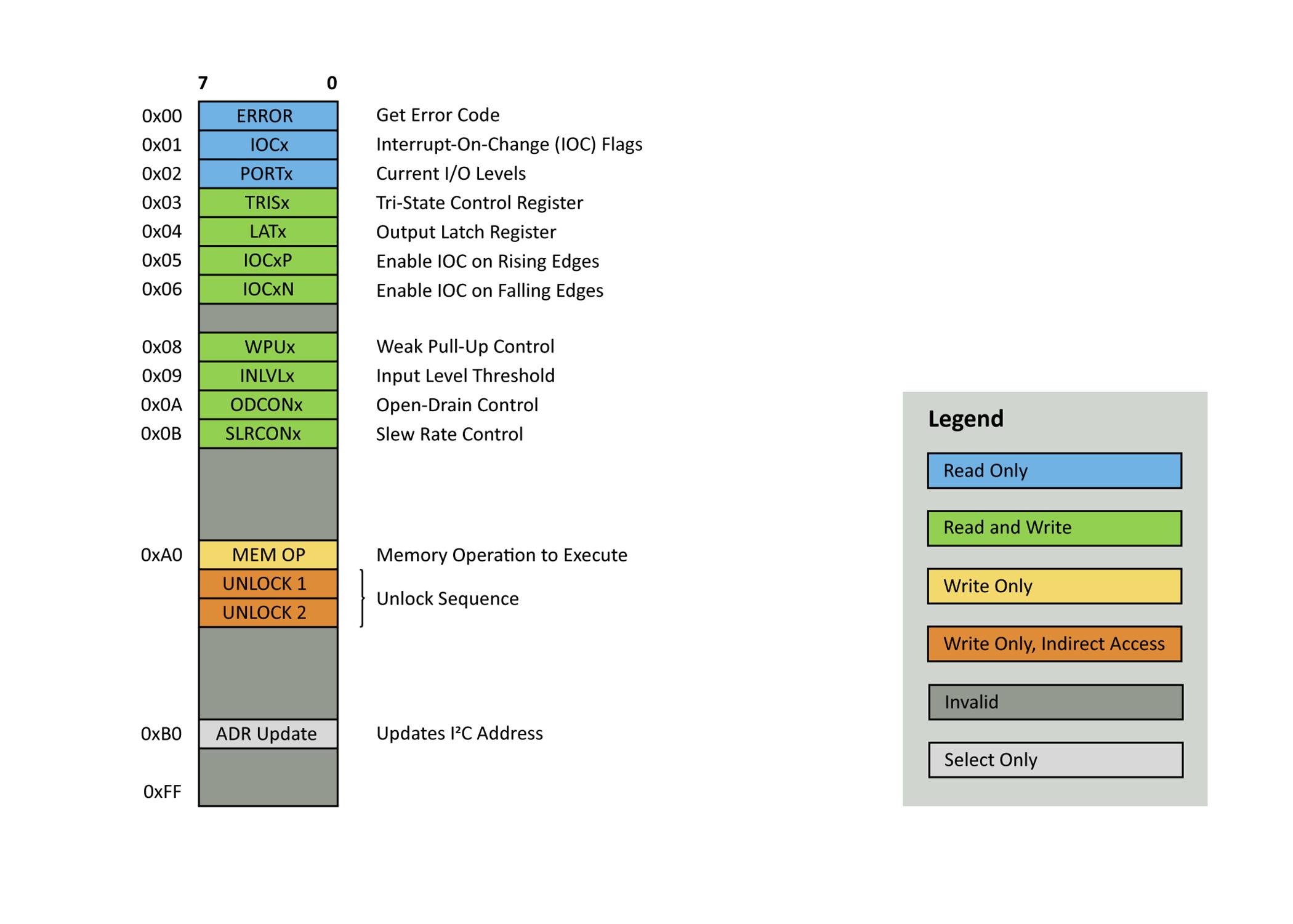
address is sent. This address does not correlate with registers on the microcontroller it is only specific to the lookup table. This means that features not in the hardware registers of the microcontroller can be added transparently Entries in the table can be easily rearranged for specific uses as well. Another benefit of this structure is the ability to add permissions to the lookup table. For instance create a read only registe omit the write lookup tabl
This more complex struct lends itself to non-standa functionalities The functi OP” allows the MCU to sa load its current General-P Input and Output (GPIO) configuration to memory
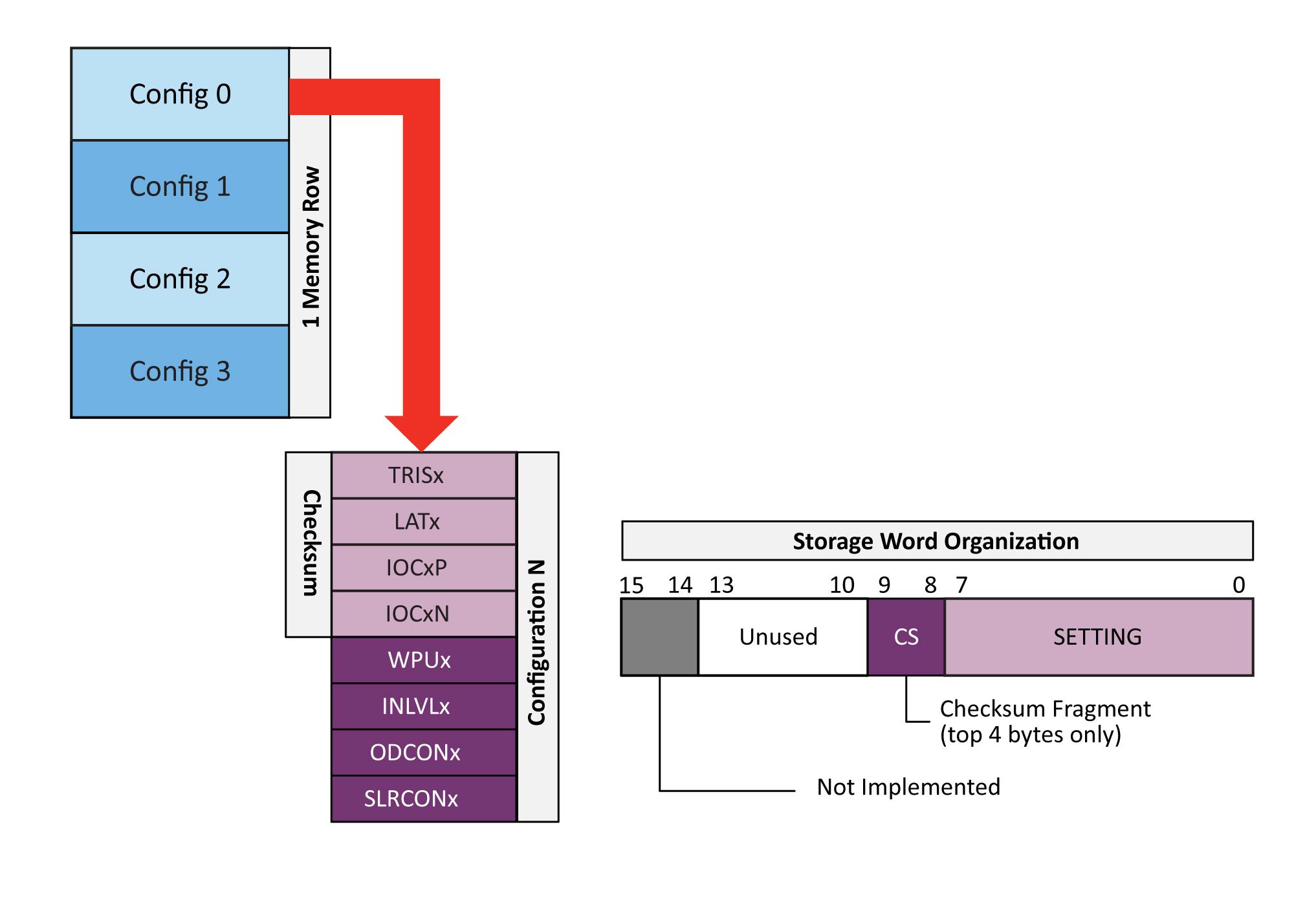
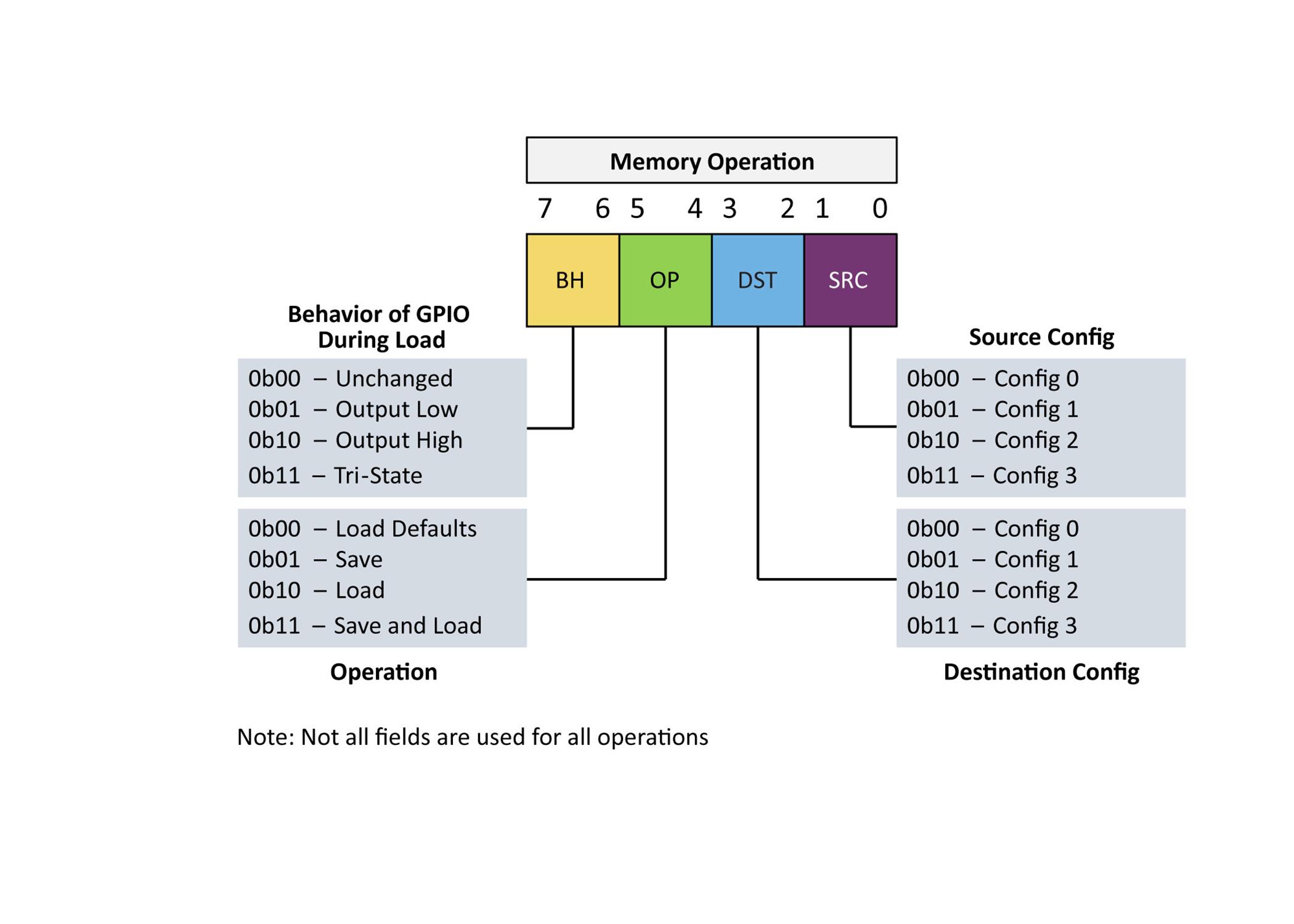
MEM OP can also reset t configuration to the param set when compiling Optionally, the microcont can be set to load the sav settings on power up If e the microcontroller attempts to load the settings in configuration 0 If the configuration fails checksum validation, then the MCU will revert to the compile time constants This feature can be disabled in the software, if not desired.
The advantage of the MCU based solution is in the extreme amount of flexibility Unlike the ASICs on the market, the MCU can be configured with non-standard functionalities specific to the application in use This application was developed for the general purpose PIC16F15244 family of MCUs
For more information about the implementation or to try out the example, please see the README files in the source
Source Code, Documentation, and Demonstrations: https:// github.com/microchip-pic-avrexamples/pic16f15244-familyadvanced i2c io expander
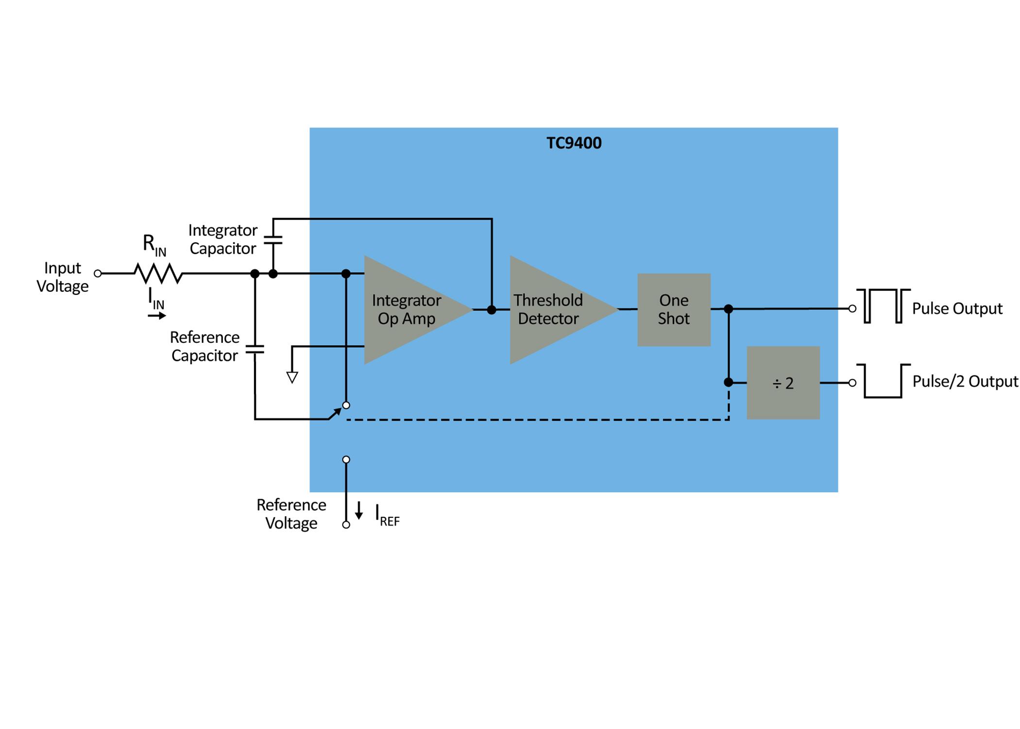
The voltage to frequency converter improves upon the traditional analog solution by reducing the Bill of Materials (BOM) and thus the design area
Many of the V/F converters on the market require external resistors
and capacitors to op whereas the microc requires generic dec pull up components all MCUs) to functio
Rather than using a techniques to digitiz uses a combination independent periphe features The MCU input signal with the Analog-to-Digital Co Computation (ADCC a clock signal to cre frequency output. In the peripherals have to operate autonom CPU after initializati means the CPU cou other tasks in the en
One challenge with the MCU based approach is that it does not perform as well as the analog solution does. The resolution of the output is intrinsically limited by the ADCC Nominally, the ADCC is 12 bits, but with the way the program is configured, the ADCC runs at an oversampled 14 bit resolution Likewise, the on-board Numerically Controlled Oscillator (NCO) that synthesizes the output frequency has finite resolution and can have jitter in its output, depending on the value measured by the ADC
The MCU based solution can be split into three distinct blocks of peripherals an analog sampling block, an output oscillator block, and a duty cycle generator
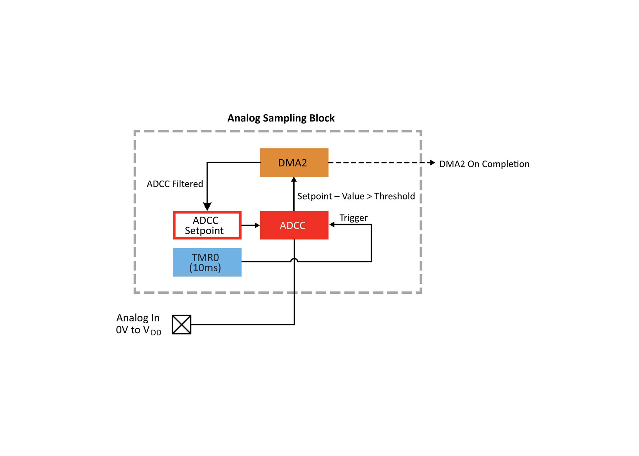
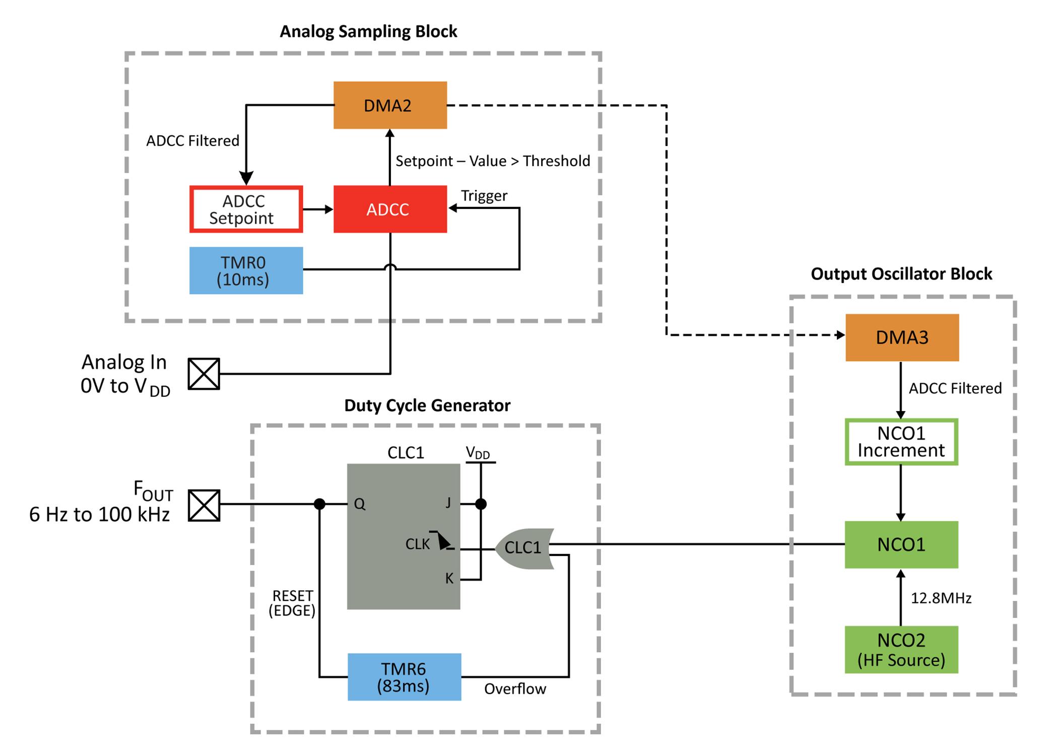
The analog sampling block is responsible for the analog to digital conversion For an output of 100 kHz to be possible with the frequency limits of the device, the ADCC has been configured to oversample, then average down to get a 14 bit result
A downside to this oversampling is the extra statistical noise added
to the result. The noise is compensated for by averaging the oversample and adding hysteresis. To implement hysteresis, the threshold interrupt feature of the ADCC is used (For simplicity, only the specifics of how this example uses the threshold interrupt feature will be covered.)
When the ADCC finishes computing the averaged oversample, the resulting value is compared to a setpoint register in the peripheral If the difference between the two is greater than or less than set thresholds, then an interrupt is triggered The CPU
masks this interrupt and is unaffected, however this interrupt triggers a Direct Memory Access (DMA) copy of the averaged oversample result to the setpoint register of the ADCC, creating hysteresis. If the thresholds are not exceeded, then the DMA copy will not occur, which will not trigger the output oscillator block’s DMA to update.
The output oscillator block of this solution is responsible for generating a clock signal at the desired output frequency This
ive 12 bit resu s not large ate the 100 kH n external cloc
Generator bloc s responsible f 50% duty cyc ure is optional he NCO can be hough the duty a much larger
connected to the duty cycle generator, which halves the frequency of the output but creates a 50% duty cycle output Due to this, the output oscillator block runs at twice the frequency of the output
The heart of the output oscillator block is a Numerically Controlled Oscillator (NCO) The NCO peripheral works by adding an increment value to an accumulator on the rising edge of an input clock. The accumulator overflow is used to derive the output of the peripheral (For the full explanation on the NCO, please consult the datasheet.)
In this example, NCO2 has been setup to internally create the required input clock frequency to get a 100 kHz output from a 14 bit input The 14 bit result is used
This generator is implemented using one of the Configurable Logic Cells (CLC) The CLCs are small blocks of discrete configurable logic, similar to a single cell of an Field Programmable Gate Array (FPGA). CLCs can be used as discrete logic gates, such as AND OR or OR XOR They can also be configured as latches or flip flops. In this solution, a CLC was implemented as a J K flip flop with Reset J and K are kept at logic HIGH.
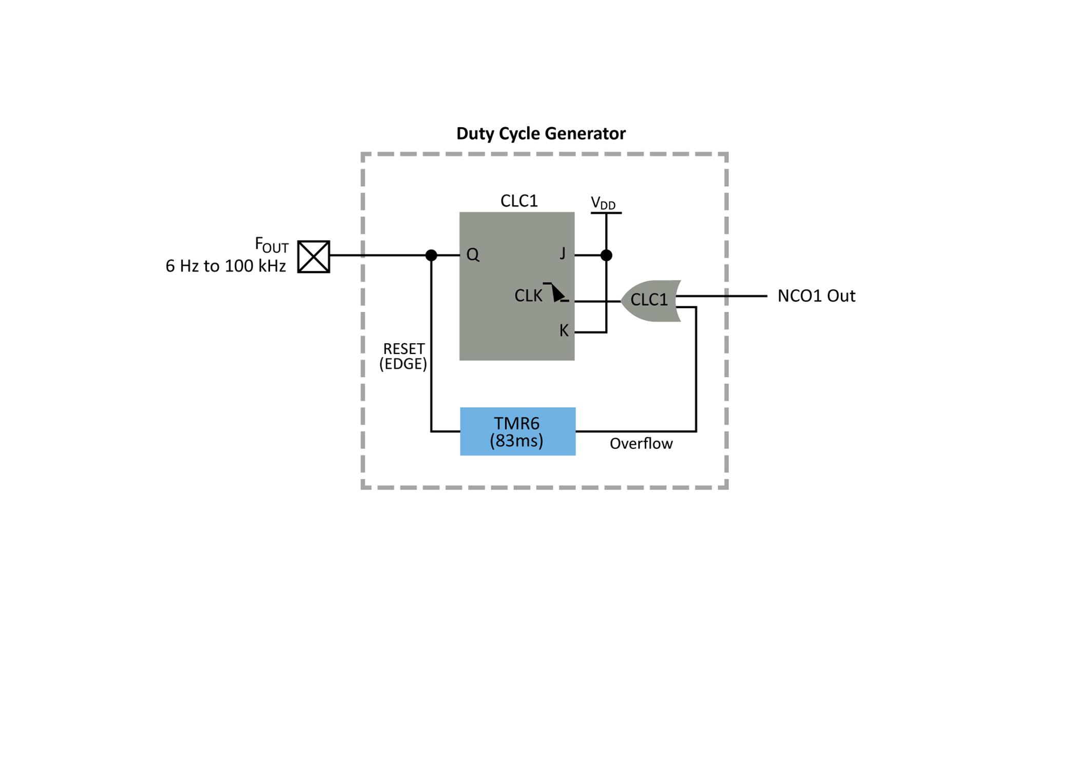
The output oscillator block is used as the clock for the flip flop Every input clock pulse causes the output to toggle, which generates a 50% duty cycle Note: frequency jitter from the output oscillator block will affect the duty cycle
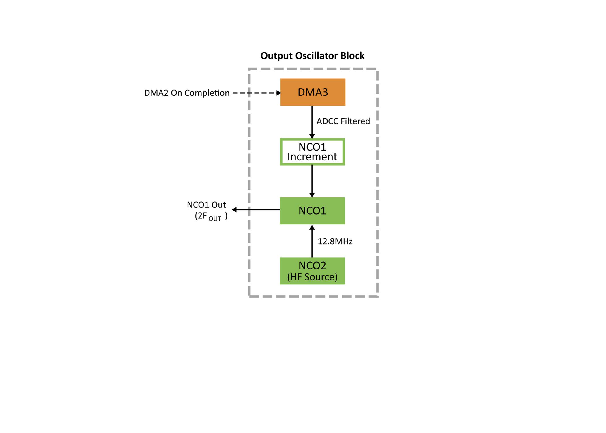
Timer 6 is used as an astable “watchdog” timer If the output does not produce an edge (rising or falling), then the timer will overflow and generate a clock pulse to the CLC. This controls the low side of the output frequency range Rather than reaching DC, the output toggles at the half of the frequency of the timer, for an output of 6 Hz
This example demonstrates the use of hardware peripherals to create a core-independent function that ordinarily would have to be created with an external integrated circuit. One of the biggest benefits to this configuration is that the peripheral operation is setup in software, making it easy to adjust the example to the end application
For implementing the example, the PIC18-Q43 family of MCUs was selected due to the large number of peripherals in use.

For more information about this example, please see the README document in the example repository. The example repository also contains an implementation of a frequency to voltage converter that can be implemented on the same device as the voltage to frequency converter.

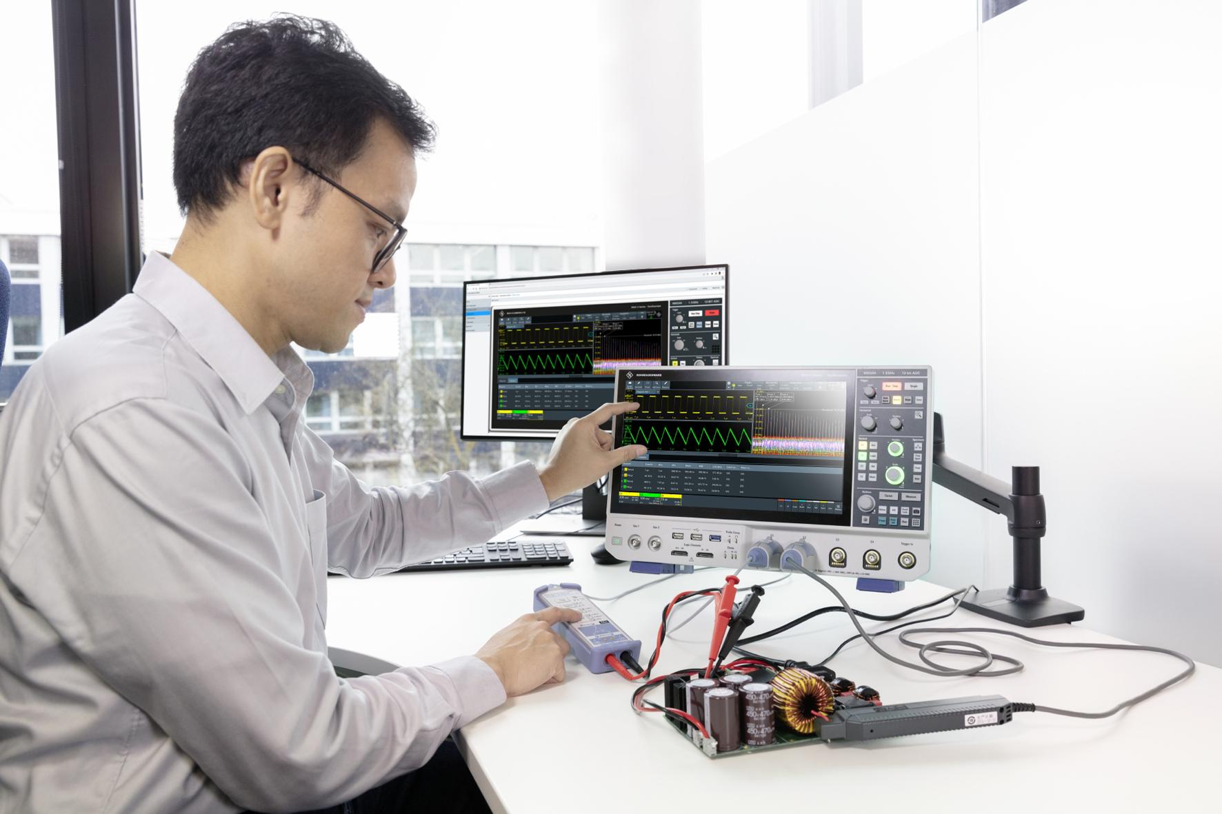
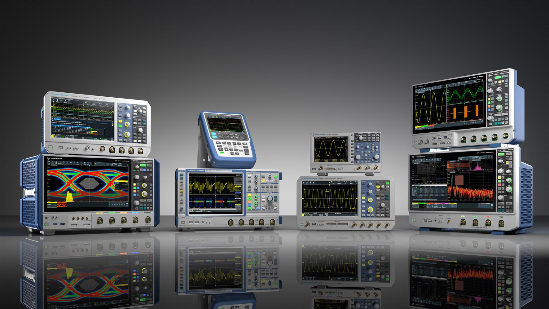
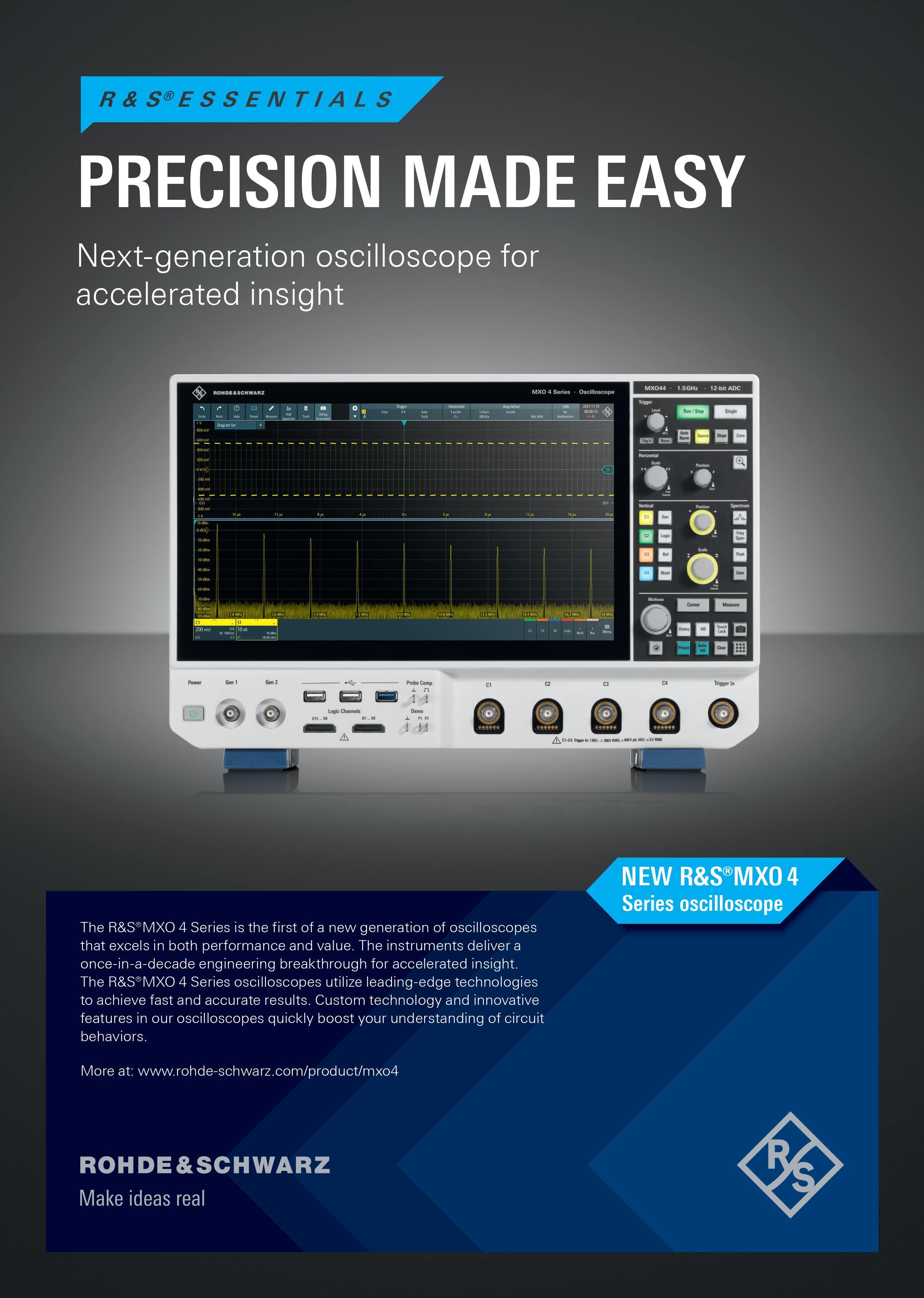
Rohde & Schwarz is extending its portfolio with the R&S MXO 4 series oscilloscopes, which are a once in a decade engineering breakthrough. They deliver industry leading hardware performance previously only available to higher performance instruments and blend in superior software functionality and value. All this to give engineers accelerated insight into their electronic designs to provide industry leading products to the market efficiently and quickly.
Oscilloscopes play a key testing role in electronic labs
While Rohde & Schwarz has more than 85 years of experience with high quality instruments equipping test labs, it wasn’t until 2010 that
the company expanded their test and measurement product range with their first digital oscilloscope, the R&S RTO1000. With subsequent additional introductions of oscilloscope instruments,
probing, and applications, the company now offers the newest portfolio ranging from 70 MHz to 16 GHz bandwidth
As a privately owned company, Rohde & Schwarz has more flexibility in making long term
deep technology investments that have resulted in a number of technology milestones (see box) on the journey to become a major player in the oscilloscope market. Today, users can choose from many different models and configuration options from the Rohde & Schwarz oscilloscope portfolio, from entry level instruments for educational applications to handheld and high end lab oscilloscopes.
Much of the innovation was exclusive to the higherperformance class of instruments However, now
Rohde & Schwarz adds a completely new oscilloscope series to its portfolio, the R&S MXO 4 series, which brings all the performance from its upper class to the mid-range and even delivers a number of industry firsts The new R&S MXO 4 series oscilloscopes come in four channel models, offering bandwidth of 200 MHz up to 1 5 GHz It is the first of a new generation of instruments that excel in both performance and value delivering a once in a decade engineering breakthrough for accelerated insight What are the benefits?

The new R&S MXO 4 oscilloscope features the world’s fastest real time update rate exceeding 4.5 million waveforms per second, showing more of a signal’s activity than any other oscilloscope A high update rate increases the likelihood of detecting and displaying signal faults and including them in the overall analysis (see Fig 1). This not only enables development teams to see and isolate infrequent events more
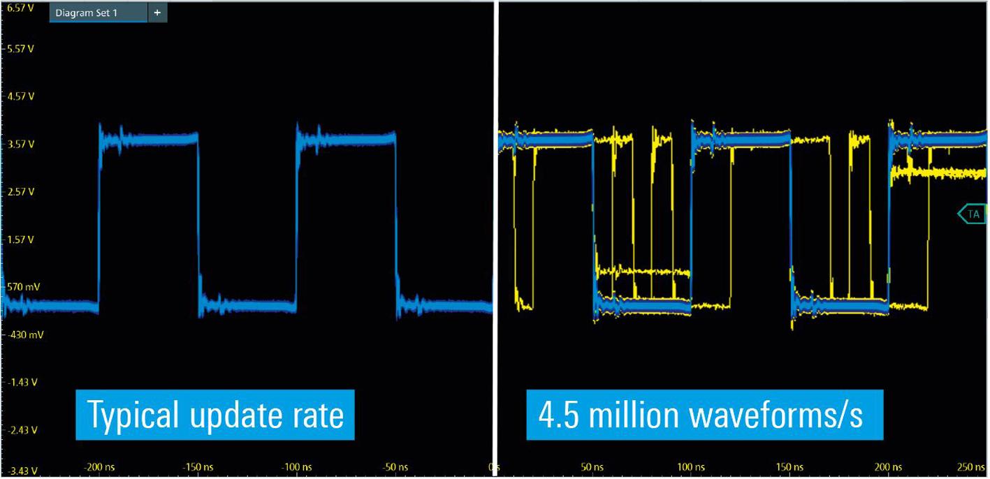
quickly, but get a better understanding of their designs and ultimately shorten testing times.
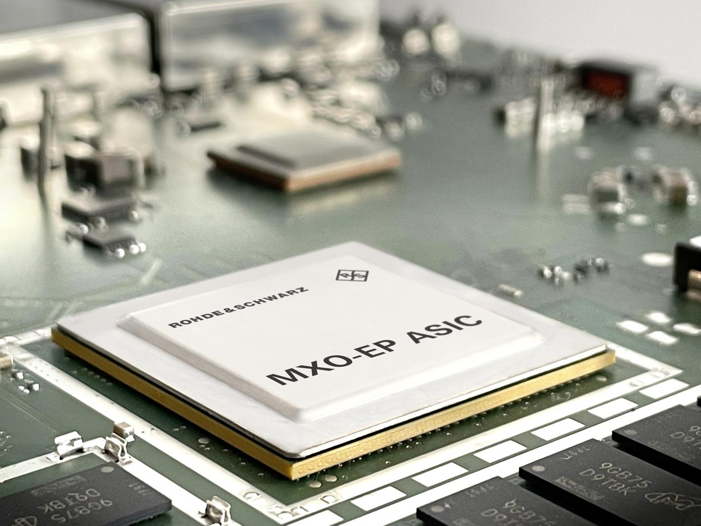
This feature, which is unparalleled in the industry, was made possible with a unique 200 Gbps processing ASIC (MXO EP, see Fig 2), one of several new technology blocks developed by Rohde & Schwarz engineers and implemented in the R&S MXO 4 Series for the first time
High update rate, however, would be of no use, if the overall instrument was sluggish and unresponsive. The R&S MXO 4 maintains a fast update rate even when complex functions are active such as automated measurements, spectrum analysis or deep memory acquisitions. The custom ASIC based signal processing ensures smooth workflows.
All R&S MXO 4 series oscilloscopes incorporate a 12 bit ADC that operates across

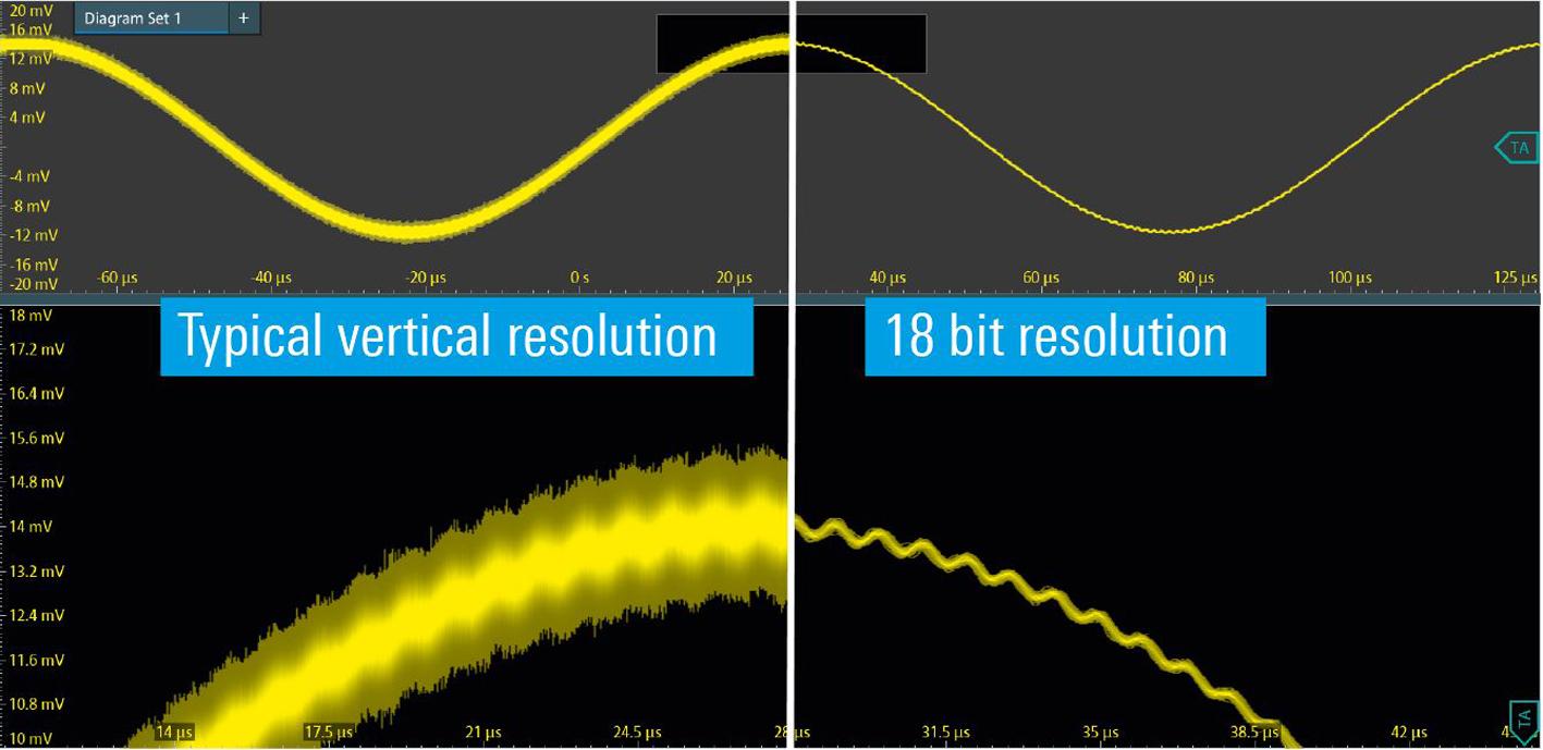
all sample rates without any tradeoffs This is a 16x improvement over a traditional 8 bit ADC architecture Going further, the HD mode implemented in hardware for speed, achieves up to 18 bit vertical resolution which allows users to see more signal details that would otherwise be masked by noise (Fig. 3). In addition, the R&S MXO 4 offers the lowest noise of just 22 µV AC (RMS) at 1 mV/div
The new oscilloscope offers an outstanding sensitivity down to 500 µV/div without any unexpected reduction in
bandwidth. It offers the largest offset range, +/- 5V with a 500uV/div scaling on 50 Ohm path without any special probes, in its class to enable users to easily place the signal at the center of the screen. These attributes enable users to see DC and other signals with more precision than with any other oscilloscope in the market
Besides bandwidth and sample rate, memory depth is the most
important attribute that determines an oscilloscope’s ability to handle a large range of troubleshooting tasks More acquisition memory gives oscilloscopes the ability to capture more time and retain rated bandwidth information with slower time base settings. With a standard acquisition memory of 400 Mpts on all four channels simultaneously, the R&S MXO 4 Series offers up to 100 times the standard memory of the primary competition. The additional memory also provides extra measurement capability when needed.
The R&S MXO 4 oscilloscope additionally offers segmented memory as standard to efficiently capture signals of interest and ignore the times of inactivity. Examples include laser pulses, streams of serial bus activity and RF pulses. With History mode available all the time, users can dial back to see previously captured acquisitions or segments For customers interested in analyzing power up/down behavior or analyzing larger time intervals an optional memory extension turns on 800 Mpts across two channels.
Triggering enables reliably capturing and displaying signals of interest. Nearly all scopes in the market have analog technology. The measured signal is split into two paths, one for viewing the signal, and a separate for triggering The analog approach doesn’t allow users to trigger on small signal
changes, and applying filters to the trigger signal are limited. Rohde & Schwarz made triggering digital with a single signal path that encompasses both trigger and signal visualization Digital triggering proved to be significantly more precise and sensitive than analog triggering It offers new possibilities for triggering on extremely fine signal details and filtered waveforms that previously was unavailable to users.
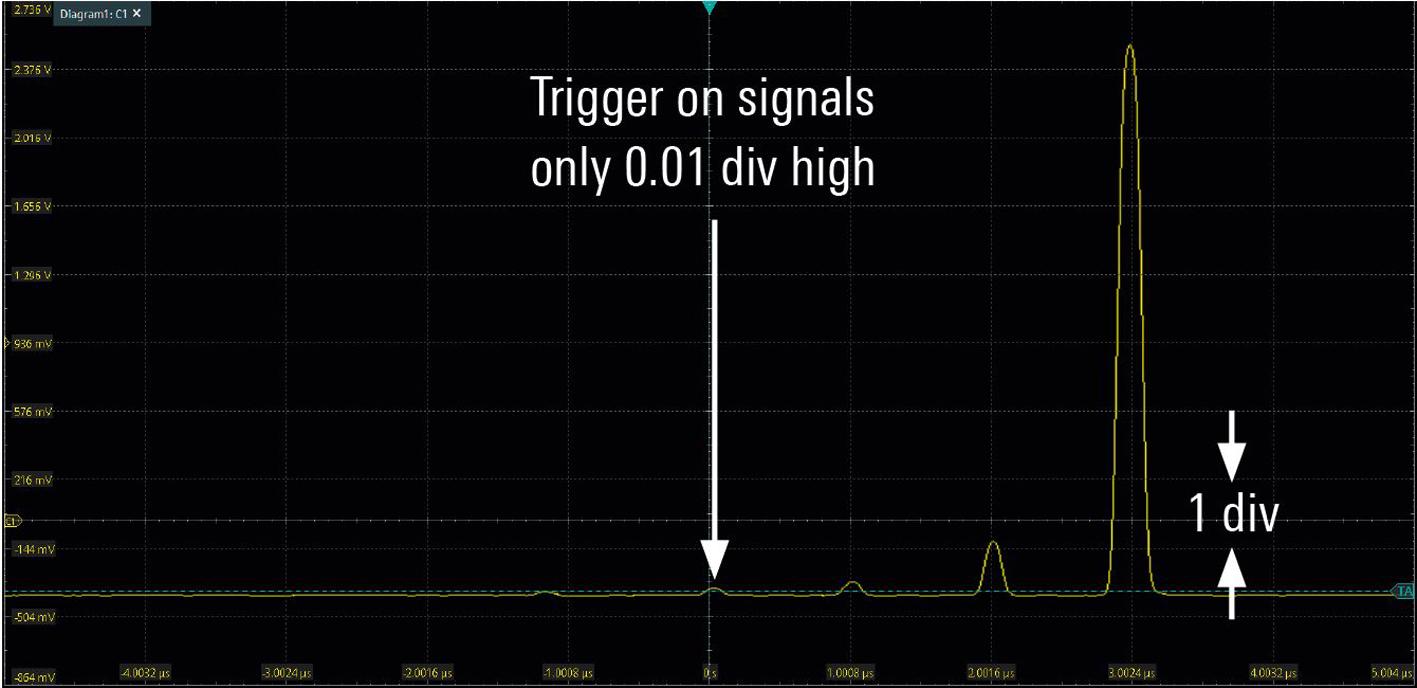
Previously only found in higher performance oscilloscopes at higher price points, digital trigger comes standard with all R&S MXO 4 Series oscilloscopes Realized with the MXO EP ASIC, digital triggering implies a common path for the measurement signal and trigger versus a spli path in older analog trigger architectures. With a trigger sensitivity of 1/10 000 division, it can isolate difficult-to-find small physical layer anomalies in the presence of large signals (Fig 4) No competitive oscilloscope has this degree o trigger sensitivity for isolated small signals. The digital trigger complements the 18 bit vertical architecture, giving
users the ability to fully utilize the precision offered by the R&S MXO 4 Series.
Full access to control all trigger hysteresis settings is another advantage with digital triggers This provides greater flexibility for determining where to trigger, including how much trigger noise suppression is desired. All this while still maintaining a very short trigger rearm time of down to < 21 ns.
Many engineers who develop products need to debug in test
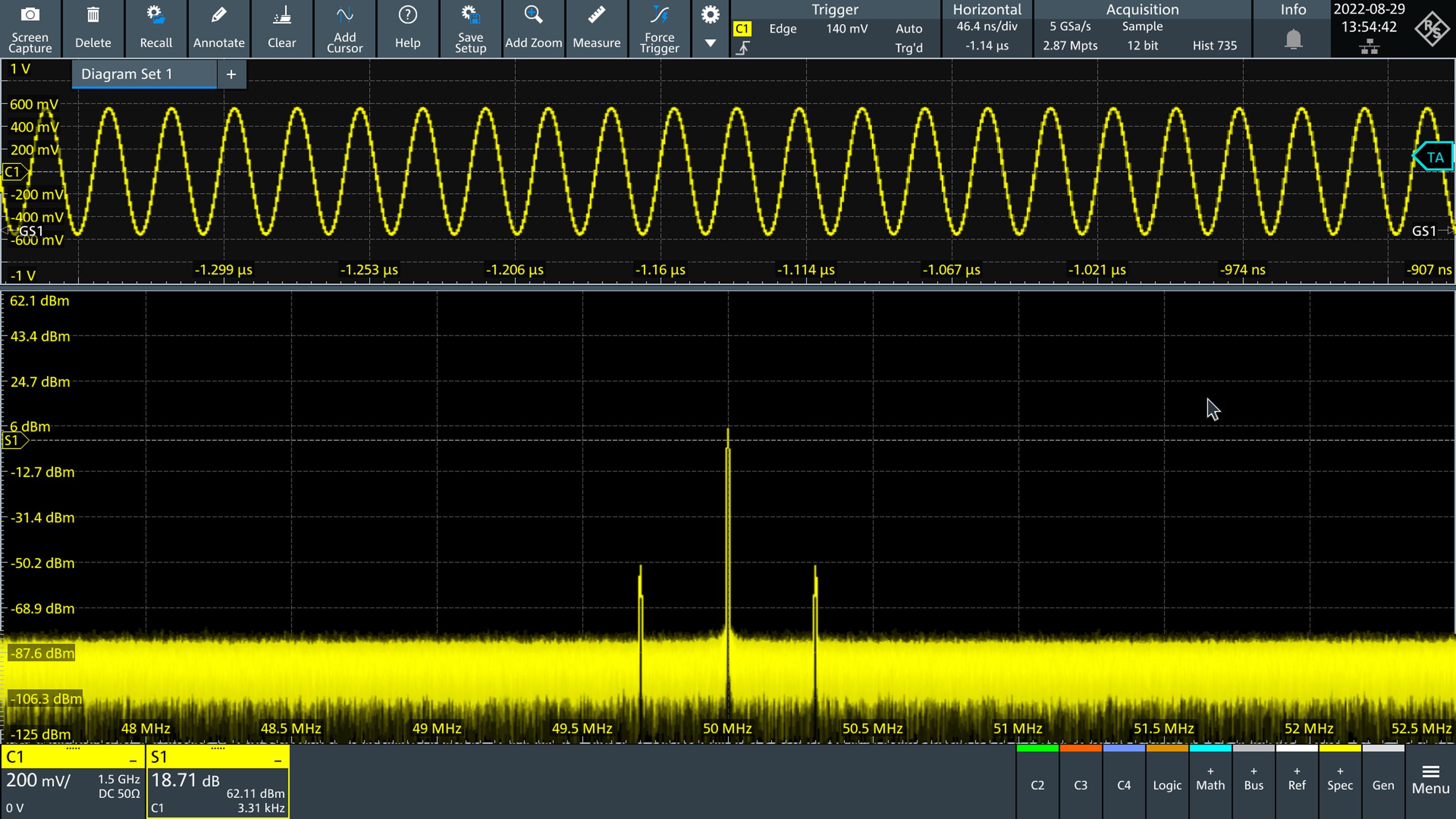
both in the time and frequency domain The designers of the R&S MXO 4 were very cautious to keep spectrum analysis in mind to bring forward fast and powerful analysis capabilities. The instrument is the first oscilloscope ever to achieve 45 000 FFTs (Fast Fourier Transfers) per second, while comparable oscilloscopes deliver less than 10 FFTs per second This allows capture of spurious spectrum events, especially when performing EMI debug, fast and easy (Fig 5).
Configuring the spectrum function on the R&S MXO 4 has been made simple by entering common parameters such as center frequency, span or resolution bandwidth (RBW). These settings are independent of the time domain settings, however still time-correlated.
A variety of additional functions and measurements are included to make it easier to plot and gain quick insights from the spectrum.
The pristine RF characteristics of the R&S MXO 4 balances great spectrum performance with the synchronized time domain view This capability is included in the base instrument, allowing engineers better visibility of RF signals than with any other oscilloscope in its class.
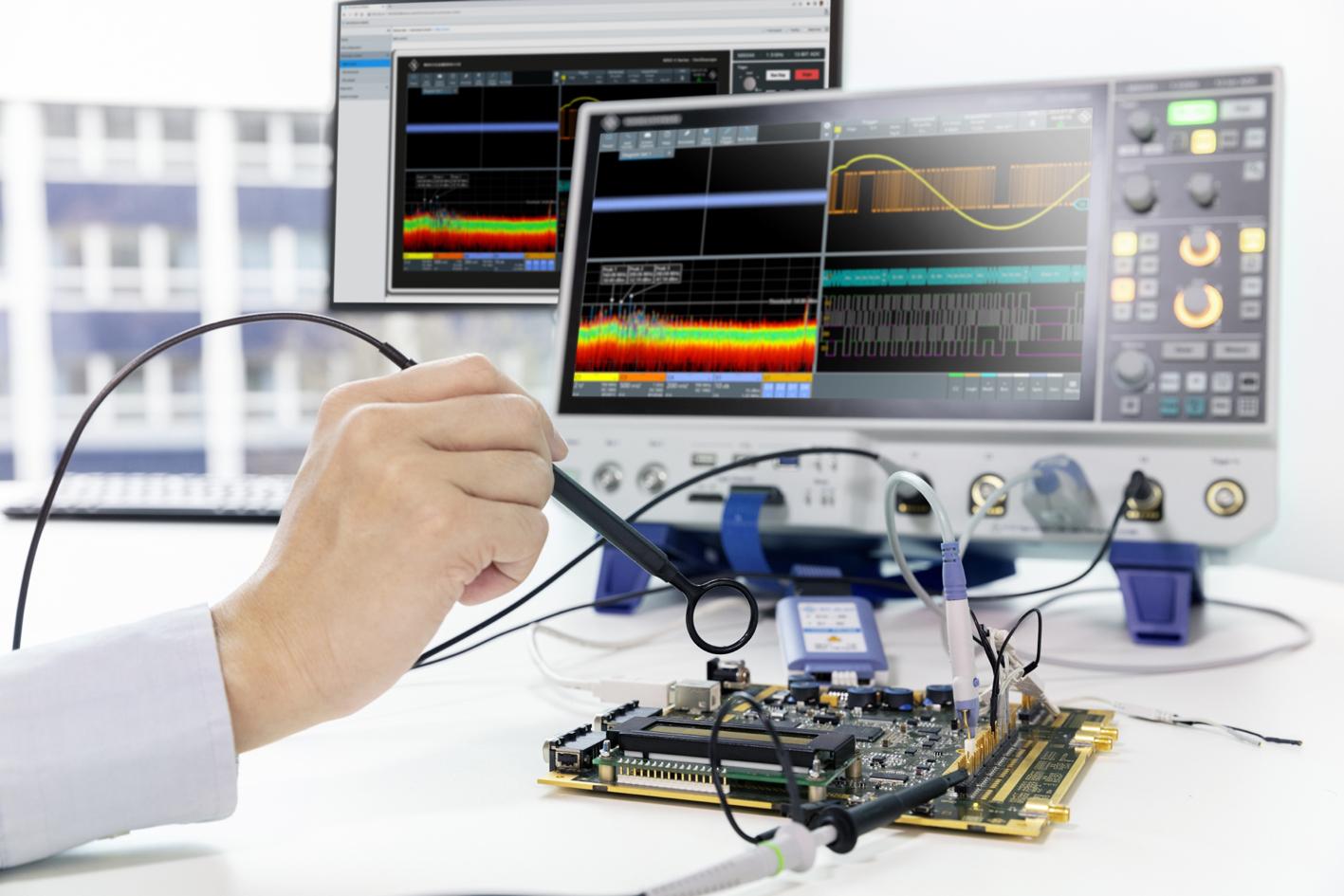
Using an oscilloscope is a visual experience and users spend significant time viewing the instrument’s display. The R&S MXO 4 Series incorporate a 13.3” full-HD capacitive touchscreen featuring gesture support and an intuitive user interface (UI)
Extensive user feedback and research into the smart device user interface concept led to the development of the R&S MXO 4 series UI. Maintaining close contacts with users and evaluating new usability techniques in mobile touch products outside test and measurement, led to a
well-structured workflow that allows users to focus on the task at hand, rather than learning a new instrument The user interface design was architected for a key user requirement to maximize waveform viewing, even when setting dialogs are open.
Its straightforward box design provides enhanced touch ability by allowing users to touch any part of the setting field to change a parameter The larger touch targets make it easier to work effectively. Alternatively, a mouse and/or keyboard can be used for operation.
Efficiently organized toolbars give quick access to important and most used functions The intuitive R&S SmartGrid, previously only available on higher performance oscilloscopes, lets users set an individual waveform layout to view all that is important.
The instrument’s small footprint, low audible noise
• In 2010, Rohde & Schwarz, known for it solutions expanded into the time domain launch of its first oscilloscopes These m changed the world of oscilloscopes:
• 2010: First real time oscilloscope with a precision trigger system enabling triggeri signal details that eluded traditional analo
• 2010: Industry’s first 10 GHz single cor converter enabling the best RF measurem highest SFDR.
• 2010: Industry’s lowest frontend noise o oscilloscope for accurate results
• 2010: Industry’s first custom ASIC that waveforms/s to quickly find signal faults.
• 2012: First oscilloscope with an integra analysis like FFT to deliver effective RF d
• 2014: First oscilloscope with up to 16 b resolution allowing the ability to isolate e you can see
• 2015: First handheld oscilloscope offeri ADC and lab performance in a rugged, p with isolated inputs.
less than a whisper, and VESA mounting and a rackmount kit for installation in integrated environments make the
R&S MXO 4 oscilloscope ideal for any engineering workspace.
For users with more demanding needs, a number of upgrade options are available These include 16 integrated digital channels with a mixed signal oscilloscope (MSO) option, an integrated dual channel 100 MHz arbitrary generator, protocol decode and triggering options for a variety of industry standard buses, and other options to extend the instrument’s

ROHM introduces a compact evaluation kit to demonstrate the high performance of the company’s 4th generation SiC MOSFETs in a state-of-the-art Totem Pole PFC. In addition to showing key performance metrics such as efficiency measurements the paper describes some design challenges of the topology at hand and how they were addressed in order to obtain a PFC with universal input.

The Totem Pole PFC (TP PFC) topology as such has been discussed in multiple articles in the past [1]. With the availability of WBG semiconductors that feature high performant body diodes it is becoming very attractive Its key advantage over the traditional boost PFC is that it eliminates low frequency rectification and the power loss associated with the forward drop of a 50 Hz rectifier. Thus, efficiencies above 98% can be achieved and, if a suitable
secondary stage with a similar efficiency is used, the 80+ Titanium target efficiency can be reached.
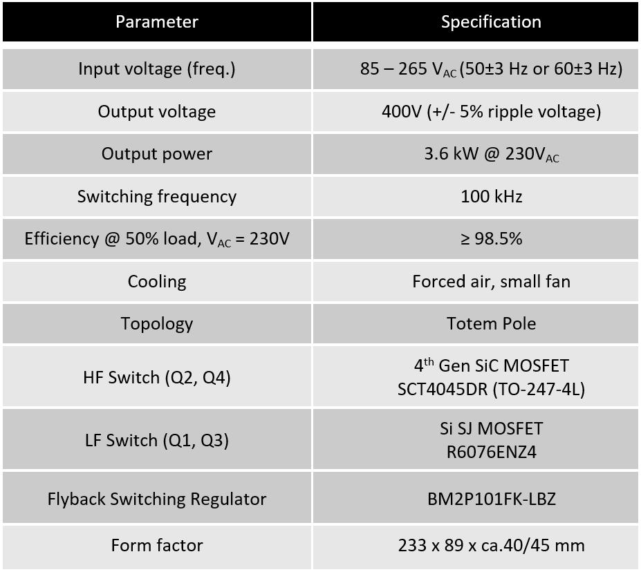
In Figure 1, a picture of the featured evaluation kit (EVK) that implements the TP-PFC with rated input current of 16A is provided alongside some of the design specifications The key devices in use in this board are highlighted in Figure 1. In addition to 4th Generation SiC MOSFETs this design uses ROHM Si SJ MOSFETs,
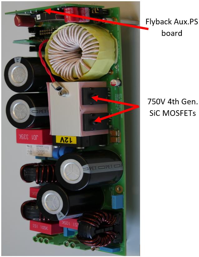
as well as the gate drivers BM61S41/BM61M41 and other components from ROHM, such as the shunt resistor and the flyback switching regulator IC in the auxiliary power supply
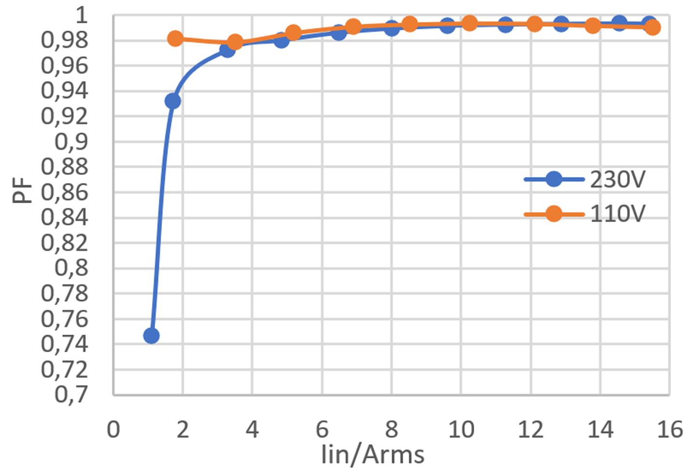
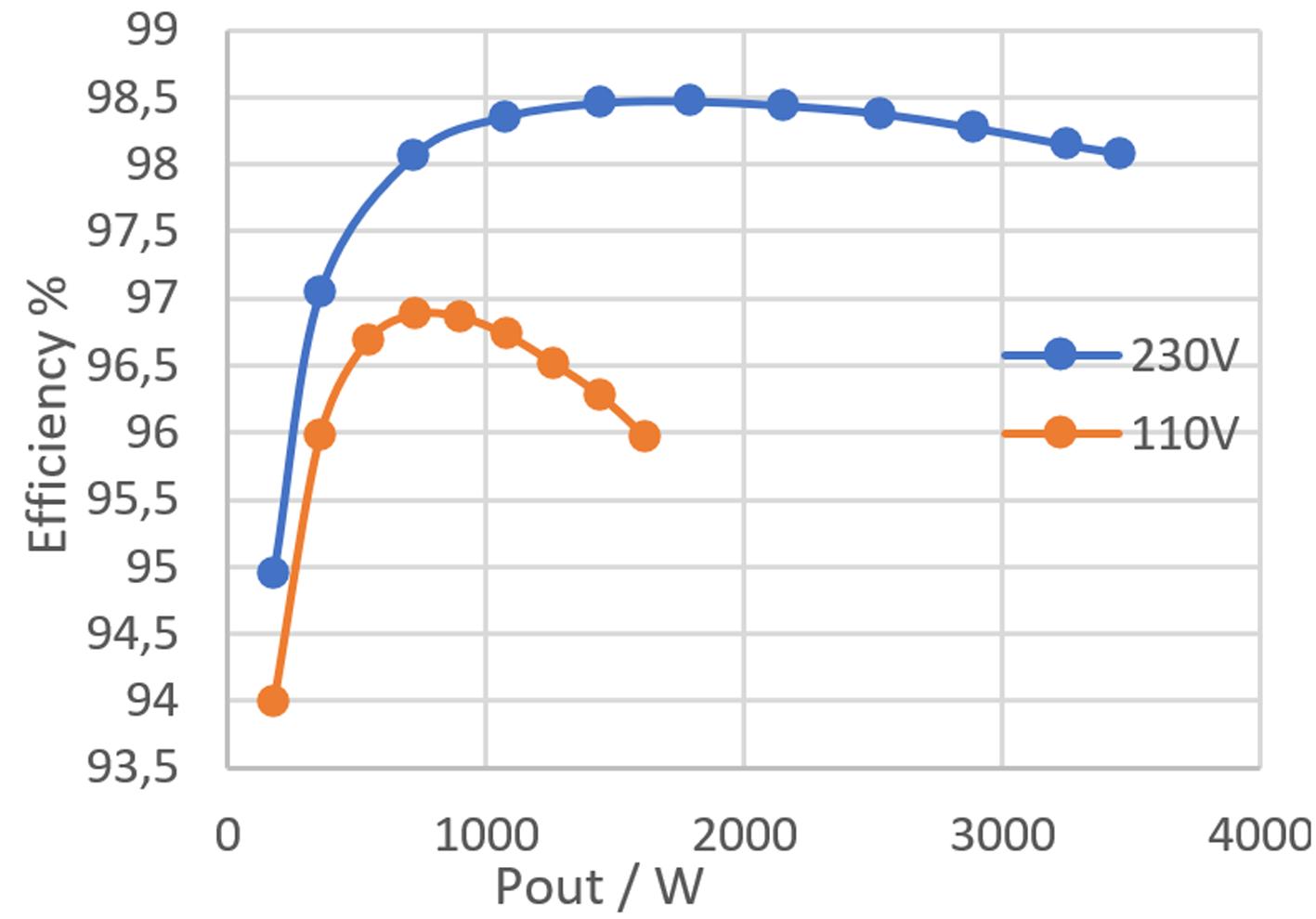
The performance of the developed EVK is illustrated in the following plots showing the measured efficiency and the achieved input power factor at both 230V and 115V AC input Regarding the efficiency, it should be noted that this includes all on board power consumption of the auxiliary power supplies for the gate drivers, the low voltage electronics, and the cooling fan It can be seen that the requirement of a power factor > 0 95 at 20% load is reached
If the PFC circuit is combined with a DC/DC stage of suitably high efficiency the design can also meet the efficiency requirements of 80+ Titanium.
The following paragraphs discuss how this design has been developed and how certain challenging aspects of this topology were addressed.

Amongst these challenges are:
• Finding the correct settings for blanking and deadtime
• Safe automatic start up on the grid's universal input voltage.
• Soft start around the AC zero-crossing to minimize current spikes
Beforehand, the benefits of ROHM’s 4th generation SiC MOSFETs are going to be highlighted.

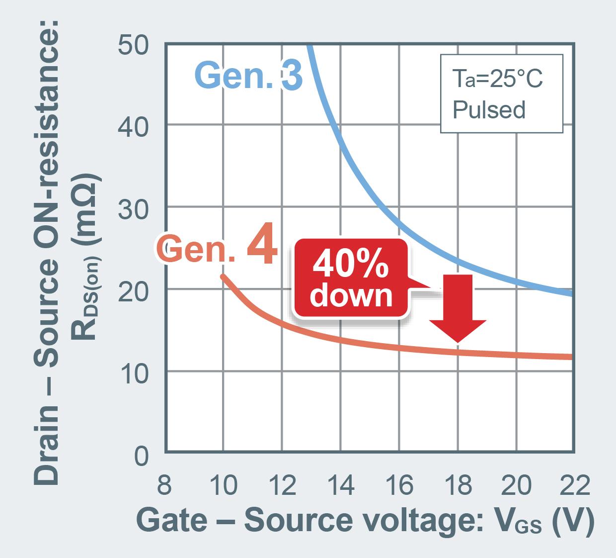
The new SiC MOSFETs realize a substantial reduction of 40% in the on state resistance per unit area compared to the 3rd generation SiC MOSFETs.
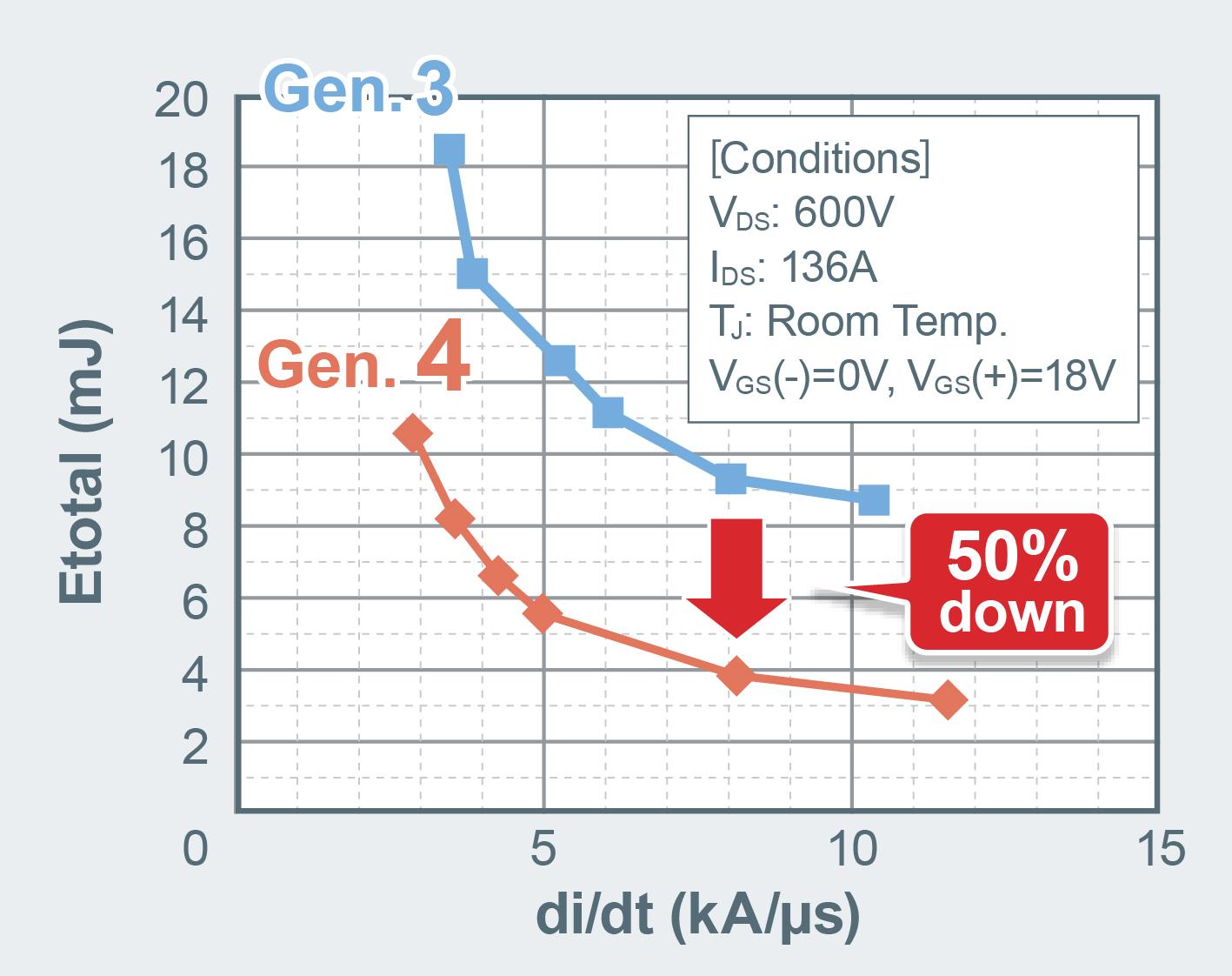
This reduction is achieved without sacrificing short circuit robustness making the new devices extremely high performing and robust. In addition, the switching losses in the 4th generation SiC MOSFETs are 50% less than in the 3rd generation thanks to a drastically reduced gate-drain parasitic
capacitance “CGD” This translates to a higher conversion efficiency
For driving the gate, in contrast to the 18V gate source voltage “VGS” required in the 3rd generation and earlier SiC MOSFETs, the new products support a more flexible gate voltage range (15 18V). In addition, due to the reduction in the “CGD” parasitic capacitance and hence the CGS to CGD ratio, the 4th generation SiC MOSFETs can be safely turned off with just 0V without parasitic turn on that may be caused by a high dVDS/dt. As a result, the gate driver circuit can be simplified by eliminating the need for a negative bias for turn off.
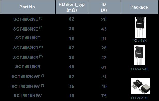
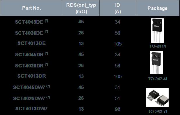
Table 1 shows ROHM’s 750V and 1200V 4th generation SiC MOSFET line up The devices
are available in THD through hole TO 247N and TO 247 4L as well as in the SMD version TO 263 7L. The automotive qualification is planned for all devices marked with an asterisk (*).
The errors associated with the AC zero crossing detection as well as the parasitic elements of the MOSFETs must be taken into consideration when setting the PWM control In this TP PFC EVK, a 50µs blanking time has been inserted around the AC zero crossing During which, the four switches are turned OFF shortly before the zero crossing, either from positive to negative or from
shoot through The control loop is frozen during this time to prevent the integrator build up from causing an unwanted high current spike by applying a large PWM pulse in the next turn on. A short blank time enables higher controllability over the current waveform, lower THD and relatively higher efficiency However, the minimum blanking time is limited by the controller sampling rate and the line frequency.
In addition to the blanking time around the AC zero crossing, a suitable dead time must be set between the control commands of the complementary SiC MOSFETs. From the BM61S41 gate driver datasheet the propagation ax
65ns Adding another 10ns max for the PWM propagation mismatch results in an absolute minimum dead time of 75ns. To account for the turn off and turn on delays of the SiC MOSFETs and to have some margin, the dead time for this board was set to 150ns Of course this needs to be evaluated for each design and is also impacted by the selection of turn on and turn off gate resistances.
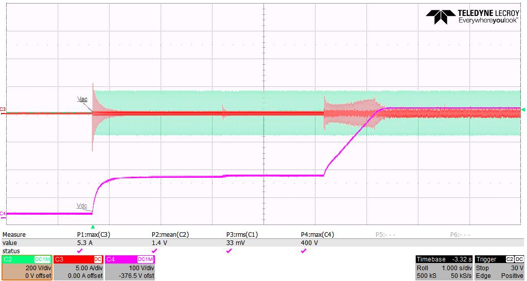
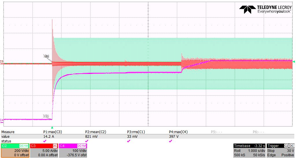
The TP PFC EVK is equipped with a PTC for pre charge in parallel with a bypass relay. At start up, the relay is turned off and the bulk capacitors are pre-charged through the PTC
turning on the relay and operating the converter This prevents a circuit damage due to high inrush currents The EVK was tested over the full universal input range [85Vac 265Vac] and has been proven to be safe for an automatic start up even at 265Vac. Thanks to the implemented Second Order Generalized IntegratorFrequency Locked Loop (SOGI FLL), this EVK is also able to track and detect drifts in the grid’s frequency of 50±3 Hz or 60±3 Hz.
In the TP PFC topology, the MOSFET’s switching sequence is of the essence. A failure to understand and observe the control challenges in a TP-PFC can lead to improper operation, unexpected EMI issues or even failure of the power devices. The most common challenge that is inherent to
this topology is the occurrence of current spikes at the AC zero crossing [2],[3] These are mainly caused by the output parasitic capacitor “COSS” and the associated reverse recovery charge “Qrr” of the line frequency switched MOSFETs, which are only changing state on the AC zerocrossing. A detailed analysis of the AC current spikes and waveforms in a TP PFC topology is presented in [2]
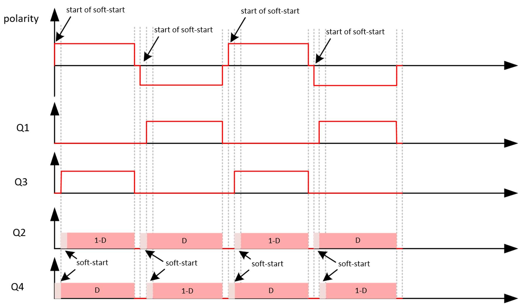
In ROHM’s TP PFC EVK a soft start sequence is implemented after every AC zero crossing. This involves a ramping of the duty cycles applied to the high frequency SiC MOSFETs (Q2, Q4) and fine control over the turn on of the low frequency Si SJ MOSFETs The implementation of this soft start achieved significantly reduced current spikes. The implemented MOSFET’s switching sequence is shown in Fig 6
The MOSFETs Q2 and Q4 are complementary switched.
During the negative half cycle, the Q2 MOSFET is the active switch which is controlled by the calculated duty cycle “D” During this time, the Q4 MOSFET is operating in synchronous rectification mode at “1 D” duty cycle. Note that the Q1 MOSFET is only switched at the grid’s frequency and stays on during the full negative half cycle to provide a low impedance return path to the mains The operation reverses again during the positive half cycle and the high side and low side MOSFETs of each leg interchange their function.
As the input voltage changes polarity from negative to positive half cycle, and right after the AC zero crossing, the soft start sequence of the Q4 MOSFET kicks in. This sequence consists of applying an increasing factor to the pulse width in a way that gradually increases the on time of this MOSFET from 0% to 100% of the calculated “D” cycle While doing this, the Q1 MOSFET completely reverse recovers and the “VDS” of Q3 reduces to ground. Thus, the positive current spike, caused by the slow recovery of Q1 and the high “VDS” voltage across the Q3 MOSFET, is eliminated.
Knowing that the AC voltage is very low right after the zero crossing and since the inductor is already charged to the DC bus voltage, a large negative reverse current will flow through the inductor back to the mains. This leads to a high negative current spike when turning on the Q2 synchronous MOSFET even at “1-D” duty
cycle. Therefore, once Q4 reaches the full “D”-cycle, the soft start is also applied to the Q2 synchronous MOSFET to reduce this negative spike to near zero Simultaneously, as Q2 softly starts, Q3 must be turned on to provide the current path back to the mains.
A large negative current spike will also appear at the AC zero crossing if the Q3 MOSFET is turned on too late after the soft start of Q2 is completed as detailed in [2].
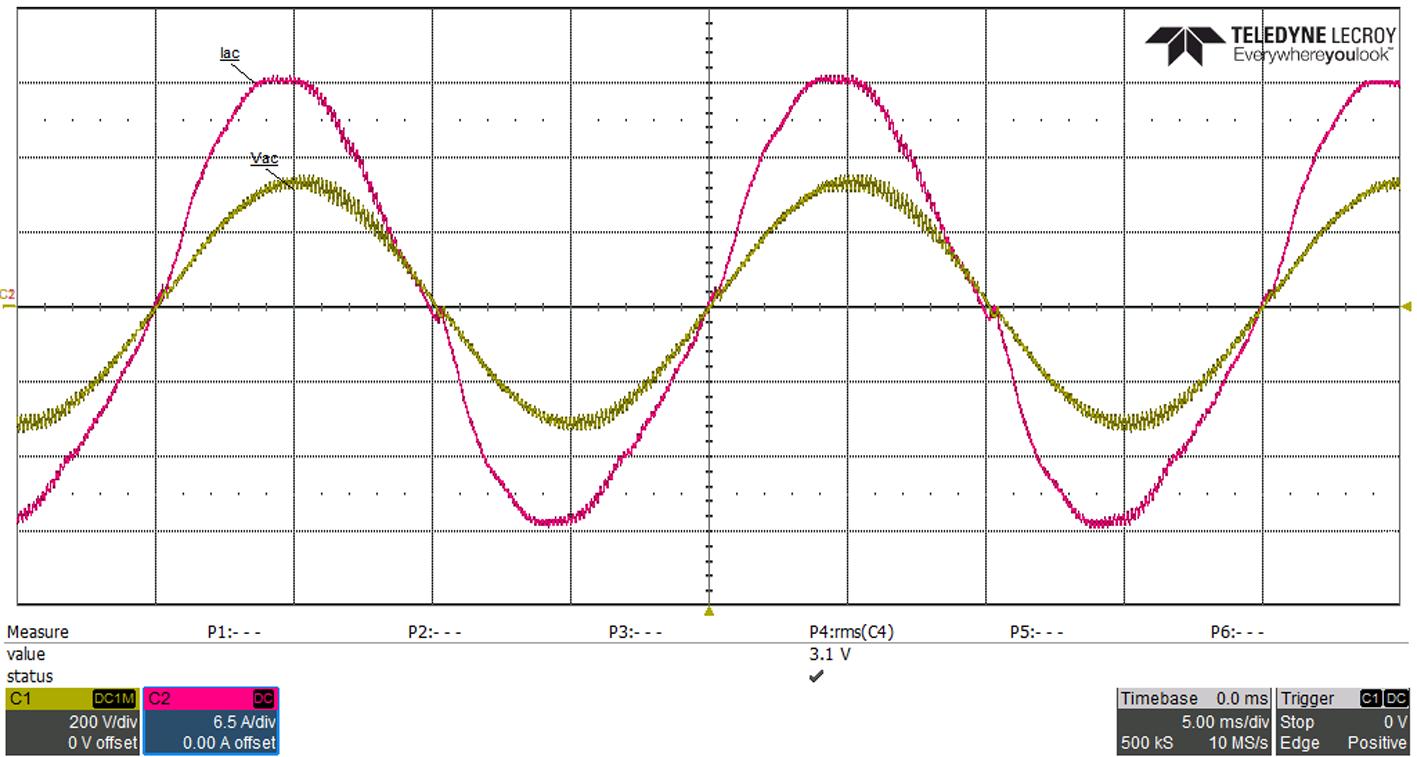
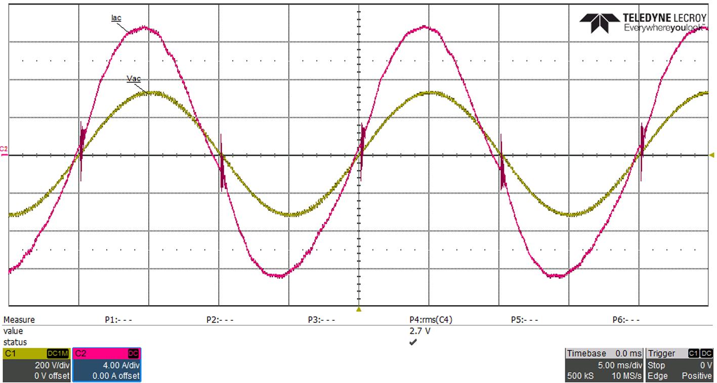
Figure 7 shows the input current waveform around the AC zero crossing with and without the soft start.
Note that, since the ''1-D'' is very small when Q2 first turns on, it becomes even smaller and tends to zero when
The MOSFETs’ control sequence explained in the previous section was implemented and tested in the 3 6 kW TP PFC EVK From the test results, without this control method, both negative and positive current spikes are present. The application of the soft start to both active and synchronous MOSFETs, as well as turning on the low frequency MOSFETs at the right moment, has shown better current waveforms and helped achieved much lower THD.
The presented TP-PFC EVK shows a high performance in major design aspects, including control features and a high efficiency, reaching 98 5% while including all on
board power consumption of the auxiliary power supplies and the cooling fan Both low on state resistance and low switching loss of the 4th generation SiC MOSFETs helped in the achievement of such performance.
The results demonstrate how suitable these new products are for many power conversion applications such as for example server and data center power supplies, telecommunication, industrial power supplies (SMPS), energy storage systems as well as inside electric vehicles (e.g., OBC) where high power density, efficiency, simple gate circuit and short circuit robustness are required
multiplied by the soft start factors. Depending on the used gate driver, Q2 may stay off for a couple of PWM cycles until the ''1 D'' term becomes larger than the gate driver’s minimum PWM on time. This results in a remaining, but very small, positive, and negative current spike at each AC zero crossing.
MACHINE LEARNING AT THE EDGE
Many customers fail to assess and demonstrate the benefits AI will bring to their application. To jumpstart applications on the right foot, STMicroelectronics´ Edge AI Sprint brings a whole support system of experts that can guide developers through the minefields inherent to their application and use case

Traditionally, large companies looking to benefit from machine learning must hire one or more data scientists to collect a massive amount of data for months, clean them, and create AI models. Embedded developers then port the implementation on microcontrollers or use dedicated tools to convert neural networks into optimized code for MCUs
When a company wrestles with tight budget constraints, hiring one or more data scientists may be out of the question. Additionally, it may not be possible to outsource the job. Some situations are sensitive, while others require

someone to be constantly on staff
Even with the right people and all the time in the world, obtaining quality data is still an issue. Despite all the advances in machine learning, getting reliable training samples can be a severe problem. For instance, if an application tries to detect abnormal behaviors, data may be unavailable Indeed, while many datasets work for classification problems, such as anomaly detection, they’re useless when trying to detect new situations. It is also critical to obtain good quality data, which is far from obvious. When samples aren’t plagued
by typos or missing information, recording clean sets and precisely labeling them can demand serious investments
NanoEdge AI Studio is a utility that speaks to embedded developers, even to those with no data-science expertise. The magic lies in running the training phase that learns a complex nominal behavior and the inference on the same device The entire process can thus run on the same STM32 microcontroller. Additionally, the end user interaction can be simple, like pushing a button. As a result, engineers can customize their system to its local environment, making it
more robust and easier to install
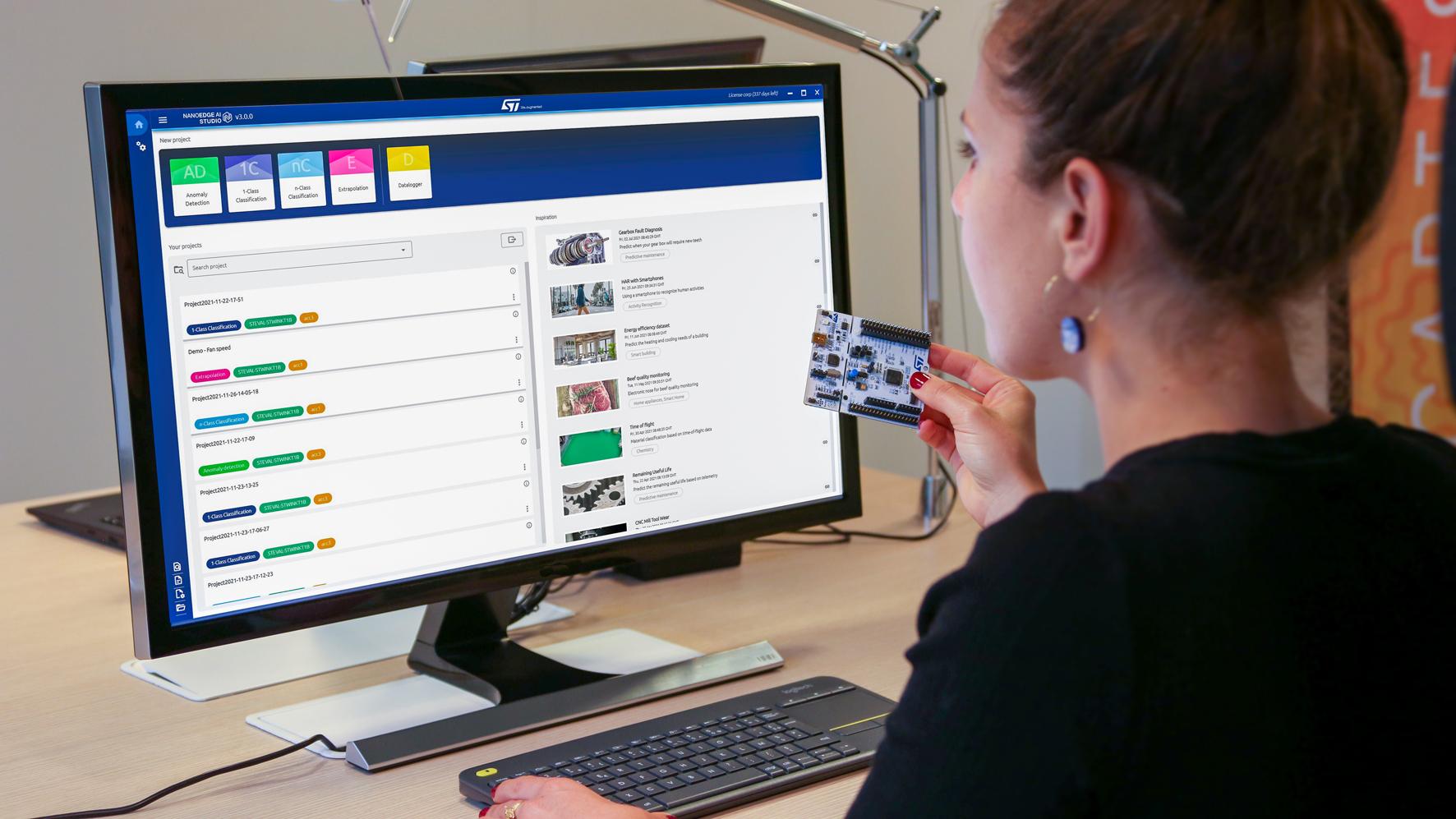
NanoEdge AI Studio runs on Windows 10 or Ubuntu and is the best way to process data as well as find the most pertinent AI libraries. The application’s design focuses on embedded development and seamless integration in C applications Put simply, NanoEdge AI Studio considers basic specifications like CPU, memory, sensors, and searches for the best NanoEdge AI library. It then outputs a library running on STM32 MCUs that developers can directly integrate into their embedded applications And with today’s update, the utility offers more libraries as well as data logging capabilities
The latest version of NanoEdge AI Studio expands the number of machine learning algorithms: in addition to anomaly detection and classification, it also offers two new families of algorithms: extrapolation and outliers The former helps anticipate behaviors in untested conditions. Also called regression, it maps the relation between multiple variables. For example, data sets could measure a fan’s behavior at 100ºC, 110ºC, and 150ºC Now, thanks to a regression algorithm, the machine learning application can extrapolate the behavior at 160ºC. The extrapolation algorithm in NanoEdge AI Studio doesn’t only cover linear regressions. Indeed, it also offers more advanced analysis techniques to tackle complex situations As a result, developers can now create
new applications that monitor things that data scientists cannot test themselves.

The second algorithm is an outlier detection system that rests on a single class of values Indeed, the system only learns normal behavior. Anything that deviates from it becomes an anomaly. Previously, when using the anomaly detection system, developers would record normal behavior, then simulate one or more problems As mentioned, it was possible to learn all behaviors on the same microcontroller, thus vastly simplifying operations. However, in some cases, reproducing anomalies is simply impossible Hence, outlier detection can use data from routine operations to infer an anomaly in such a situation
Data scientists may run against the imperative to release the final product to market and may be stuck. Indeed, while there’s no better data than the one from real world usage, it is not always available Additionally, many
are time constrained. Hence, the new data logging feature turns any STWIN SensorTile wireless industrial node into the most straightforward data collection tool Users connect the board to their PC and use NanoEdge AI Studio to switch to data logging. Afterward, recording data becomes automatic. Engineers can fix the STWIN board to their equipment to monitor it. The sensors will record data that developers can then label and parse to create more accurate applications
Another vital improvement in the new version of NanoEdge AI Studio is the user interface. With the arrival of new algorithms and data collection features, it was critical to improve the user experience It was also crucial to optimize developers’ workflow
Indeed, NanoEdge AI Studio targets teams looking to bring machine learning to the edge. The libraries are tiny as little as 1 KB and highly optimized It was thus necessary to also improve access to algorithms to ensure
developers can easily select their project category and rapidly generate their libraries
Before the advent of NanoEdge AI Studio, engineers had to contact software vendors, go over their hardware configuration, and the behavior to monitor Today, the tool enables developers to customize, generate, and validate their machine learning library. The utility first asks users to select their Cortex M architecture and the sensor in the system. They then import a file with values describing the equipment’s typical behavior It can be data from an accelerometer on a fan or the electrical information of industrial equipment

Afterward, NanoEdge AI Studio automatically tests, optimizes, and sorts the best algorithmic combination among hundreds of millions of possible combinations and produces a customized library that developers can validate using the embedded emulator NanoEdge AI Studio V3 now supports all ST development boards right from its user
interface The availability of optimized and free libraries thus means that running a proof of concept is straightforward For instance, in the smart vibration sensor tutorial, users can grab the NUCLEO-L432KC to capture a fan’s normal behavior.
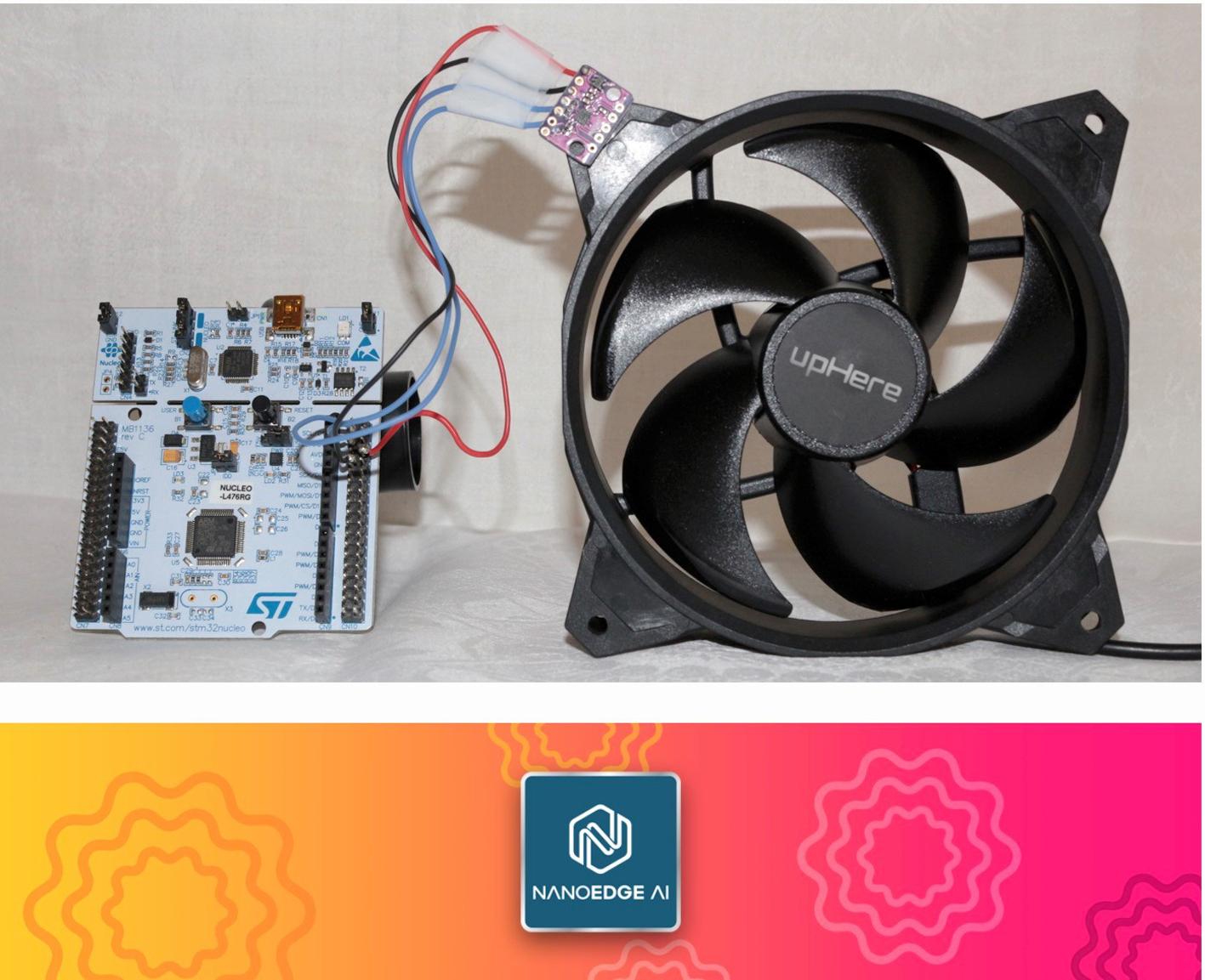
They then feed the data to NanoEdge AI Studio and obtain a library that they can call in the main loop to run a minimum number of training cycles previously defined by benchmarks within the new software before engaging in inference Hence, NanoEdge AI libraries can rapidly help create applications that use
Holding a Nucleo board in front of NanoEdge AI Studio.
predictive maintenance, smart security operations, and more Many customers fail to assess and demonstrate the benefits AI will bring to their application. Hence, to jumpstart applications on the right foot, Edge AI Sprint brings more than just a utility but a whole support system of experts that can guide developers through the minefields inherent to their application and use case. Edge AI Sprint is thus a bundle that includes training sessions, a NanoEdge AI Studio license, and technical support Teams can select from various license duration, depending on their projects’ complexity, to ensure they can reach production. Meant to bootstrap a project’s first steps, Edge AI Sprint thus limits risks and investments while increasing the chances of success
Communication of data between various devices is essential in many aspects of daily living. The proliferation of devices and the dramatic increase in data volumes driven by digitalisation and Industry 4 0 are forcing changes in the communication
networks that support connectivity across entire factories are required. Data must be extracted from operational technology (OT) machines, processed, and then supplied to computer systems at the company level (IT) for further processing As the previous 4mA to 20mA or

With this standard, it is possible to continue using existing 2-wire cabling and thus protect investments
This article explains the basics of 10BASE T1L and shows corresponding products that are also relevant in the

selection of suitable connectors for various applications Power transmission of the various connected devices via the data line also plays an important role with 10BASE T1L.
Data communication is taking on an ever-greater role not only in the industrial sector but also in process automation
The previous 4mA to 20mA or fieldbus applications are reaching their limits due to burgeoning data volumes, and Ethernet is thus crystallising as the communication standard.
The standard Ethernet, 4-wire solution has evolved into a 2wire solution known as 10BASE T1L, consisting of a single pair of twisted cables or single pair Ethernet (SPE)
Above the physical layer, 10BASE T1L is compatible with existing Industrial Ethernet technologies with 100Mbps or 1000Mbps and thus is a supplement.
10BASE T1L is becoming standardised especially in process automation and has the potential to effect sweeping changes in this area. Precisely here, up to now, sensors and actuators have usually been connected via a 4mA to 20mA analogue interface or a fieldbus In process automation, unlike in mechanical engineering or
plant automation, these sensors and actuators are usually at a distance to the control system or the remote I/ O systems Distances of 200m to 1000m and more are common.

But what exactly is 10BASE T1L, what advantages does this technology offer, and why is it a new standard?
The name 10BASE T1L roughly explains its meaning The Institute of Electrical and Electronics Engineers (IEEE) abbreviations are used here.
The “10” in the medium type references a transmission rate of 10Mbps “BASE” refers to baseband signals, which means that only Ethernet signals can be transported over the medium. “T” stands for “twisted pair.” The digit “1” stands for 1km range In this case, it is followed by an “L” for “long range,” meaning that segment lengths of 1km and more are possible.
There are still other network technologies, such as 10BASE 2 (thin coaxial cable with a maximum segment length of 185m), 10BASE 5 (thick coaxial cable with a maximum segment length of
500m), 10BASE-F (fibre optic cable), or 10BASE-36 (broadband coaxial cable with multiple baseband channels and a maximum segment length of 3600m)

10BASE-T1L offers the possibility of using the existing 2 wire infrastructure to realise line lengths of up to 1000m at a transmission speed of 10Mbps The physical Ethernet technology is defined exclusively in Layer 1 (the bit transmission layer or physical layer) of the Open Systems Interconnection (OSI) model. Above the bit transmission layer, 10BASE T1L supports common Ethernet protocols such as PROFINET, Modbus, etc , as well as other bus systems, such as BACnet, KNX, and LON, that are commonly used in building management systems. Table 1 shows an overview.
10BASE T1L is implemented with the help of a special Ethernet PHY in Layer 1 The Ethernet frames are transmitted between MAC and PHY via the media independent interface (MII), reduced MII (RMII), or reduced gigabit MII (RGMII)
The MAC is defined by the Ethernet standard IEEE 802.3 and implemented in the data link layer (Layer 2). The PHY forms the physical interface and is responsible for coding and decoding the data between the transmission medium and the digital system.
10BASE T1L is designed to replace the 4mA to 20mA standardised signal in many, if not most, process automation applications. However, this does not mean that older field instruments connected via 4mA to 20mA current loops will have to be replaced with 10BASE T1L capable field instruments These conventional devices can be connected via software configurable I/O (SWIO) modules, while remote I/Os serve as a collection point for connection to the PLC with a 10Mbps Ethernet uplink
Software configurable I/O modules have reconfigurable module channels which allows them to work quickly, easily, and remotely without requiring extensive rewiring. The channels can be configured either as input or output both for currents and voltages, or digital and analogue
In some cases, there is a requirement that both power for the devices and their data be provided via 10BASE-T1L, which is defined as part of the standard Figure 1 shows an example of a mix of conventional field instruments connected via a 4mA to 20mA current loop and new 10BASE T1L capable field instruments.
10BASE T1L supports two amplitude modes: 2.4V for cable lengths of up to 1000m and 1V for shorter distances up to 200m Through the 1 0V peak to peak amplitude mode, this technology can also be used in explosion protected environments (hazardous
areas) and meets the strict maximum energy consumption requirements applicable there.
An industry consortium has specified the advanced physical layer (APL), which builds on the 10BASE T1L standard, defining intrinsically safe operation for process automation
Ethernet APL likewise enables the transition to seamless process automation installations with field-to-cloud connections, including areas with potentially explosive atmospheres for installations in the food and beverage, pharmaceutical, and oil and gas industries. Furthermore, APL also defines the power provisioning classes over the single twisted pair lines.
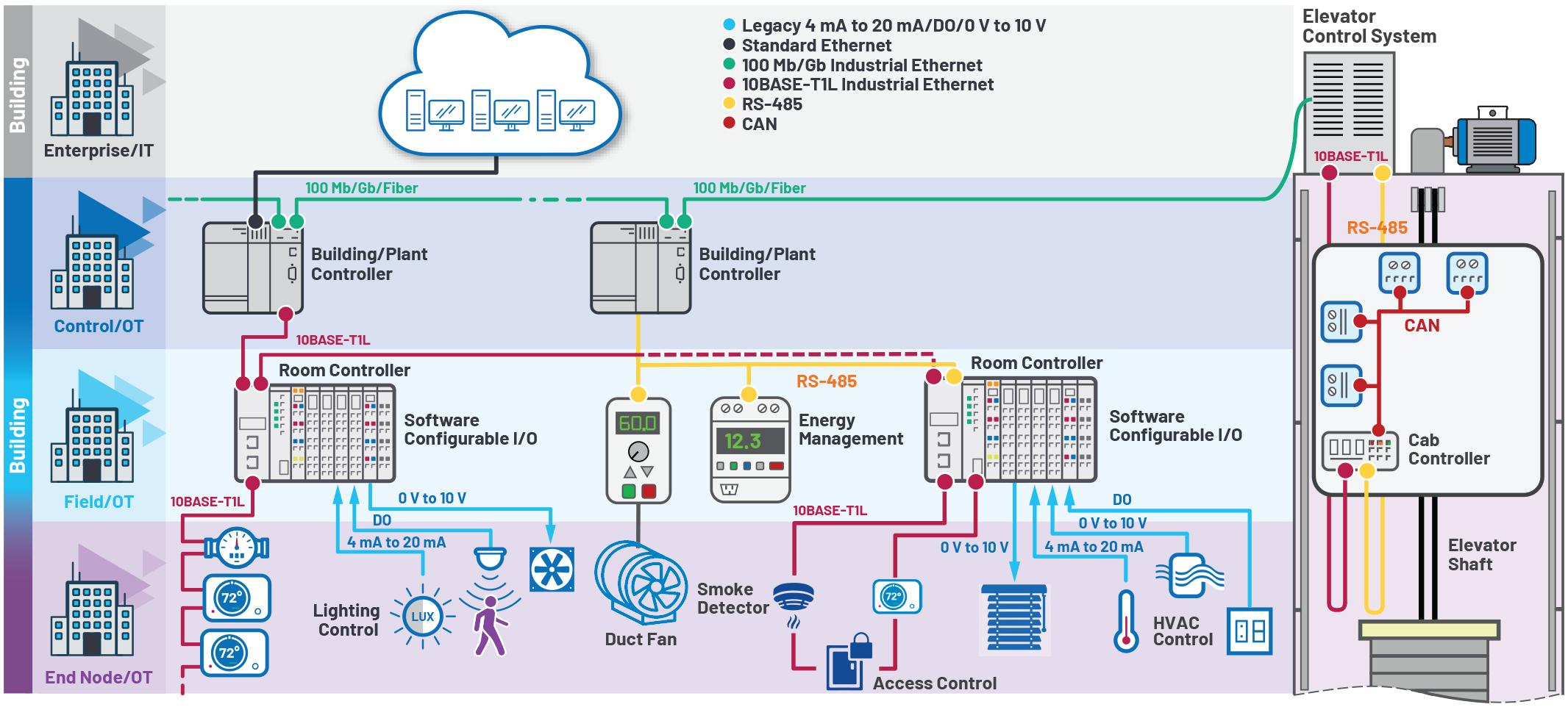
No concrete transmission medium (cable) is defined with 10BASE T1L Only the requirements for return loss and insertion loss of the cables are specified. Fieldbus Type A
cables are the cables of choice. This allows the reuse of existing PROFIBUS or Foundation Fieldbus cabling. 10BASE T1L works with a balanced pair of conductors over a cable length of up to 1000m without any problems However, in noisy industrial environments, a shielded cable like Type A cable is required using connectors, screw terminals, or punch down blocks. Some 10BASE T1L switch chips have integrated diagnostics functions that check the signal quality over the cables 10BASE T1L is thus a very robust communication technology even a mix up of the wires does not pose a problem.
Conventional 4mA to 20mA with HART® and fieldbus devices have a limited data bandwidth of just a few kbps.

With 10BASE-T1L, speeds of 10Mbps can be reached This makes it possible to transmit not only a process value but also additional device parameters such as configuration and parameterisation information. In the future, possible software updates for the increasingly complex sensors, as well as fault and network diagnostics such as short circuits on the line to the sensor, will be performed relatively quickly via the data line Configuration is also easier because gateways and converters are no longer required with 10BASE T1L. Through the elimination of the gateways, the costs and the complexity of these old installations are greatly reduced, and the data islands created by them are swept away
In addition, higher powers can be transmitted over the data line For example, 500mW in intrinsically safe areas (hazardous areas) and even up to 60W in non intrinsically safe areas can be transmitted.
Ethernet standards such as PROFINET, EtherNet/IP, HART-IP, OPC UA, or Modbus TCP, and IoT protocols such as MQTT, can enable the easy and powerful connection of field devices to a cloud.
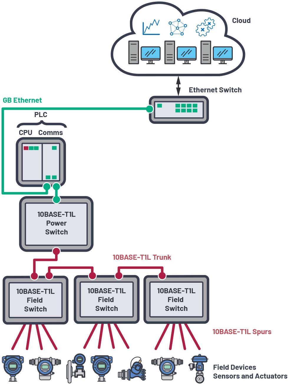
As with standard Ethernet, with 10BASE T1L there are bridges that enable coupling of various network segments and devices. Different network topologies can be realised and used to supply power to the connected devices. In process automation, switches are often connected to controllers, HMIs, and the cloud Switches allow media redundancy in the form of ring topologies for increased availability
In process automation, the connections to the devices, sensors, and actuators are also called spurs, whereas connections between the switches and running up to the control system fall under the name trunk
Further possibilities arise from the constantly increasing integration density of devices. For example, a 10BASE T1L switch can be integrated into a sensor connected directly to additional sensors that can also be supplied by it Figure 2
shows an exemplary interconnection of different switches
Communication with a 10BASE T1L capable device takes place via the host processor It usually requires an integrated MAC function, a passive media converter, or a switch with 10BASE T1L ports.
The 10BASE T1L standard not only offers communication of data from sensors and actuators, but also provides the possibility of supplying them with power via the signal lines Concretely, 10BASE T1L can deliver up to 60W of power in non intrinsically safe areas In explosion protected (intrinsically safe) areas, the power is limited to 500mW; in this case, the signal amplitude is also reduced from that of standard applications from 2 4V to 1V to comply with the strict requirements for maximum energy applicable there However, as a result, only reduced transmission distances are possible in intrinsically safe areas.
Table 3 provides an overview of the possible power transmission levels for the various line lengths and areas for a Type 18 AWG cable
10BASE T1L provides a relatively robust communication standard for process automation that offers numerous advantages over conventional 4mA to 20mA applications, including the possibility of reusing the existing infrastructure.

Batteries are crucial in the global economy transition with their ability to maintain a balance between supply and demand within the power system.

The key to decarbonize the world and fight climate change is electrification powered by renewables, which means electrification of cars (e mobility), buildings and cities. Hence increased use of solar, wind, hydropower and other low-carbon technologies, such as electric cars, storage capacity, and usage of microgrids and smart grids are the way to shift to a green economy. Electrification can help stop global warming by eliminating greenhouse emissions from the environment.
Out of all of the clean energy technologies, the focus today will be on batteries a crucial source of power in the sustainable energy future.
The article explains the importance and applications of batteries We showcase product selection from RND, a brand that provides customers with a comprehensive electronic, electrical and maintenance range of products with value and at low price, and Hy-Line, offering innovative technologies at competitive pricing

Due to the rising demand for clean energy technology like batteries, wind turbines, solar panels, or electric vehicles, it is predicted that the production of minerals like lithium, cobalt, and graphite would increase tremendously. Current technical advancements and initiatives to electrify the economy rely heavily on lithium ion (Li ion) batteries Due to their superior performance, efficiency, and
compared to ntional batteries, lith teries have become ed battery for the y of electric cars ecarbonization of the ortation industry and sing grid integration ttent renewable ene logies are both mad le by batteries’ quic n, modular design, ble installation A e (positive electrod de (negative electrode), ectrolyte serve as the ctors in lithium ion es. These batteries are currently used in everything from mobile phones and computers to electric cars They are far lighter, smaller, and better able to hold their charge than earlier forms of rechargeable batteries.
Furthermore, the costs of batteries are rapidly dropping around the globe. According to the International Renewable Energy Agency (IRENA), small scale residential Li ion battery prices, for instance, have decreased by more than 60% in Germany since late 2014.
Batteries enable utilities and grid operators to maintain the dependability of the electrical system by filling up the gaps left by the variable output of wind and solar power plants and preventing the waste of excess energy

According to IRENA in addition to providing frequency
black start capability (restoring an electric power system), and other grid functions, battery systems can also upgrade mini-grids, facilitate “selfconsumption” of rooftop solar power, and store electricity in electric vehicles
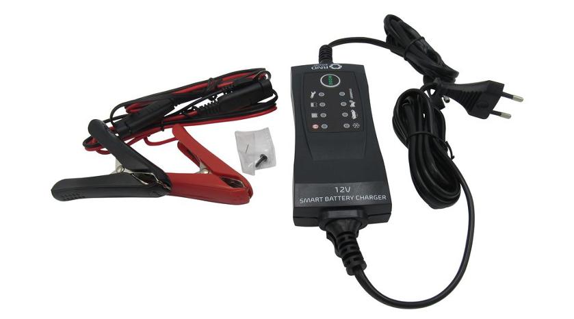
The contribution of batteries to renewable energy is particularly important because solar and wind power are still variable sources that produce changing amounts of energy When there is no wind, the sun is obscured by clouds or has set for the night, batteries can store electricity to still work. Batteries enable storing the energy collected earlier, and use it more economically
As per European Commision,
storage technology with the quickest growth rate, will be essential to achieving the EU target of a 55% reduction in greenhouse gas emissions by 2030

The percentage of battery powered vehicles is anticipated to increase significantly. Electric vehicles and the batteries that power them not only eliminate fossil fuels from our road vehicles but also increase the amount of intermittent renewable energy in grid systems. It is possible for the supply of renewable energy to outweigh the demand for grid electricity on days that are especially sunny or windy as batteries allow for the long term storage of energy
Over the past two decades, lithium ion is the most commonly used battery to charge electric vehicles.
According to the World Economic Forum, the demand for lithium ion batteries to power electric vehicles and energy storage has grown
exponentially, from approximately 0.5 GWh in 2010 to almost 526 GWh a decade later
Electric vehicles will not only be utilised for transportation but will also lower electricity costs for people who have purchased house rooftop solar panels, whether they be public, corporate, or individual investors. In fact, when electricity rates are high, electricity from parked automobiles’ batteries can be used for home purposes or
even sold into the grid.
As one rechargeable battery can replace thousands of single-use batteries, rechargeables are quite effective at lowering carbon footprint All batteries emit toxic elements like mercury, lead, and cadmium into the environment when they are disposed of in landfills, contaminating the soil and water. However rechargeable batteries are less harmful to the environment because
HY Di Smart Li Ion Battery Charger
fewer batteries are produced and end up in the waste stream. Lead-acid batteries are also the most environmentally sustainable battery technology Most of them are made up of more than 90% recycled lead
• Why are batteries important for renewable energy?
The main way to store renewable energy is in batteries. But apparently, battery development has fallen behind improvements in wind and solar power, even though without batteries these technologies work with limited efficiency Batteries enable utility providers to gather extra electricity and store it for periods when the weather is worse
• What role do batteries play in the use of renewable energy sources like solar and wind power?
In the use of renewable energy sources, batteries enable utility providers to gather extra electricity and store it for periods when the solar panels and wind turbines are not working the most efficiently (sun is not shining or wind is not blowing)
• Why are batteries crucial in the transition to an energy system with net zero carbon emissions?
Transition to a greener future will focus on renewables And most renewable energy sources use battery energy Batteries are becoming a crucial component of the sustainable transportation of the future because of advancements in battery technology. Furthermore, the power stored in these mobile batteries can be utilised to both power your home and provide grid stabilisation
• What batteries are used in renewable energy?
At the moment, most common are Lead acid and lithium ion deep cycle batteries. They are the two most important solutions for storing renewable energy
• Why is battery technology so important for the creation of electric cars?
Electric cars rely on batteries to work Electric vehicles are more sustainable because of the battery, which frees them from reliance on fossil fuels. A battery for an electric vehicle is an energy accumulator that stores electricity for
battery material, making it the energy storage technology with the lowest environmental impact
The HY Line batteries allow for monitoring of a variety of important battery parameters

HY-Di batteries offer the sumer a cutting-edge way monitor lithium-Ion battery ks from any location at any e online It is possible to se SM or CAN bus, and special HY Di Battery rface (HBI) using an rnet browser to connect to various HY Di batteries via internet.
Many people will agree that the future is electric Undeniably, soon the world will be mostly or even fully charged
electrically. Therefore, with this growing demand for batteries, there should be some plans to cut costs so that the world produces enough batteries and electric technologies
The way to achieve this is finding how to reduce the amount of metals in batteries that are expensive, difficult to obtain, or problematic because their mining has a negative impact on the environment And to shift towards the green transition society should focus on recycling, therefore improved battery recycling.
delivery to an engine using either alternating or continuous current
• What batteries are used in electric cars?
Lithium ion batteries are typically seen in plug in hybrids and all electric automobiles All electric vehicles, plug in hybrid electric vehicles (PHEVs), and hybrid electric vehicles require energy storage technologies, most often batteries (HEVs).
• How do batteries store energy?
A battery is a type of energy container that stores chemical energy to be converted later to electrical energy One or more electrochemical cells can be found in every battery Chemical reactions occur inside of such cells, causing an electron flow in a circuit This generates electric current
• How is battery energy harnessed?
A battery is an apparatus that stores chemical energy and transforms it into electrical energy. Electrons move from one substance (electrode) to another through an external circuit during chemical reactions in batteries An electric current can be created by the flow of electrons and employed to perform tasks
• Are batteries a renewable energy source?
Even though battery corrosion releases chemicals that contaminate groundwater and surface water as well as soil, the rechargeable batteries can be utilised repeatedly It means that the energy in rechargeable batteries is thus sustainably sourced, as one rechargeable battery can replace thousands of single use batteries, rechargeables are quite effective at lowering your carbon footprint
Typical single use or rechargeable batteries, such as button and lithium batteries, can be recycled, however access to recycling facilities might not be available everywhere Some batteries are recycled more frequently than others Nearly 90% of all lead acid batteries are recycled.
Due to their closed life cycle and multiple reusability, lead acid batteries are sustainable. A used automobile battery is delivered to an authorised recycler, where all of its parts are recovered, recycled, and sold to battery producers Certainly, the battery in the user’s vehicle has been and will continue to be recycled indefinitely thanks to the cradle to cradle cycle. Note that if incorrectly disposed of, lead acid batteries could be dangerous to both human health and the environment
ETNdigi is a special digital magazine from ETN. We cover components, test & measurement, radios & networks and the whole scope of embedded software. To put it short: Everything related to






design.
In 2023 we plan to publish two magazines. Want to join us? Just contact ETN editor-in-chief Veijo Ojanperä at vo@etn.fi or our sales manager Anne Charlotte Lantz at ac@etn.fi. More info about the
can be found at etn.fi/advertise


