
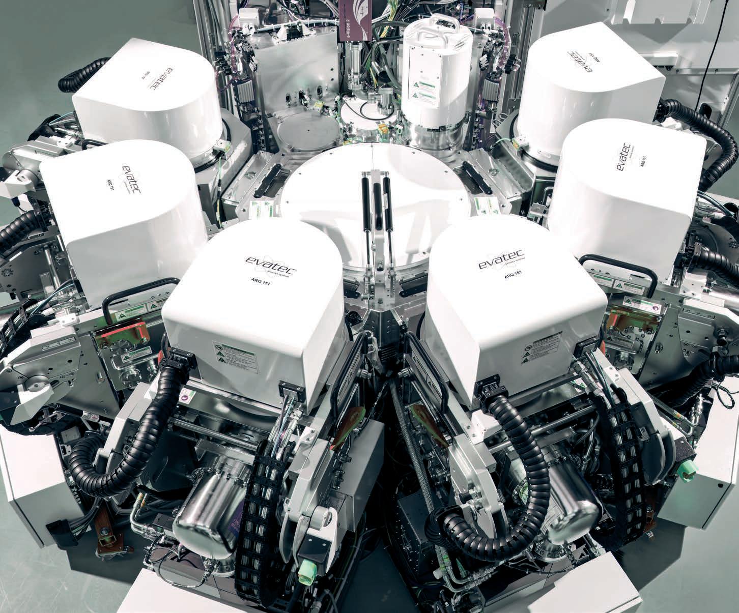
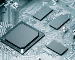
CLUSTERLINE® FAMILY
A flexible family of 200mm and 300mm cluster tools
THREE REASONS TO CHOOSE CLUSTERLINE®
1 2
PROVEN PLATFORM RELIABILITY
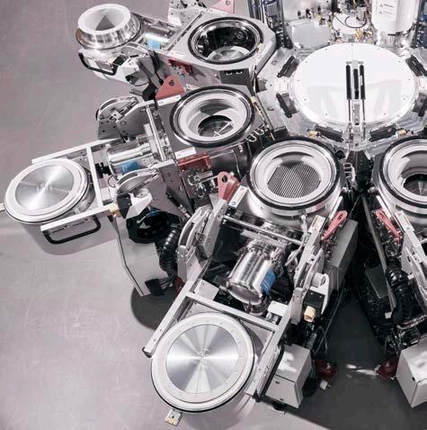
CLUSTERLINE® is a high volume single wafer processing production solution enabling integration of PVD, highly ionized PVD, Soft Etch and PECVD process technologies. Let CLUSTERLINE® do the work - from deposition of highly aligned magnetic films to high performance AlN (NanoSmooth™), or high aspect ratio TSV metallization in Advanced Packaging. You can rely on Evatec engineers to deliver proven hardware, proven processes and the advanced substrate handling capabilities you will need for today and tomorrow.
PROVEN HANDLING
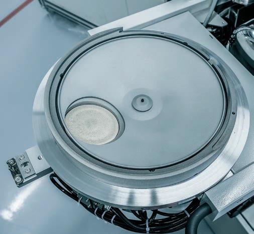
— Advanced vacuum, wafer handling and “in situ” alignment for the most accurate wafer placement in the industry

— Direct thin wafer handling down to 70μm and 6mm bow with carrier solutions for even thinner wafers
— Bridge or Split Tool capability
2
3
PROVEN PVD KNOW-HOW
Proven process capabilities come as standard when you choose CLUSTERLINE® and extensive pre and posttreatment steps can be added just as you need them.
Take a closer look at the CLUSTERLINE® family process capabilities


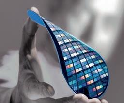
1. BAW/SAW
Extremely uniform and smooth piezoelectric AlN layers with high degree of crystalline orientation at controlled levels of stress for resonators, reflectors and electrodes, e.g. AlN, AlScN, ZnO, Ti-Mo, Ti-Pt, Al, Al alloys, W, SiO2, Si3N4, PZT
2. WAFER LEVEL PACKAGING
UBM/RDL for WLP production solutions, e.g. Ti-Cu, TiW-Cu, TiW-Au, TiW(N)-Au,TiNiV-Cu, Al-NiV-Cu at throughputs up to 60 wafers/hour
Integrated Passives: TaN, SiCr resistors, Cu coils, NiFe, CZT, laminated magnetic cores, BST/ PZT capacitors
3D/TSV (Through Silicon Via) with AR up to 15
Organic/mold substrates (Fanout, InFo) with batch degasser and low temperature processing
— Thin wafer processing on carriers or TAIKO wafers
3. BACKSIDE METALLIZATION & THIN WAFER PROCESSING
Wafer handling design assures defect-free front side
Bare wafers, thin wafers on carriers or TAIKO wafers < 50μm
Stress control, e.g Al-Ti-NiV-Ag, Ti- NiV-Ag/ Au, Cr-Ni-Ag/Au, AuAs-Ag-NiV-AuGe
Complete solution with “in-situ” pre-etch and contact anneal at 45 wafers/hour
4. LED
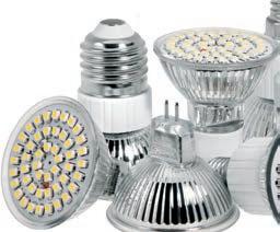
Lattice matching AlN layer (NanoSmooth™) between wafer and GaN
Metal deposition for barrier, contacts and solder materials
Passivation layers e.g. SiNx, SiOxNy
5. WIRELESS
Active compound semiconductor devices
Low temperature backside via metallization of contact layers & barriers e.g. TiWAu, AuGe, Ti/TiW(N)-Au, TiW-Al, stress optimized Cr-Ni- Au, Pt, AuZn, AuSn
6. THIN FILM HEADS
Dielectric layers, Al2O3 , AlN, SiO2, SiC, a-C
Conductive seed layers, Cr, Cu, Ta, TaN, W, Ru NiFe, CoFe, CoNiFe with magnetic alignment
7. MEMS
— System flexibility enables full process support for niche applications including sensors and biomedical applications, e.g. Ni, Pt, NiFe, NiCr, SiCr, TaN, ITO, TiOxNy and dielectrics SiC, AlN, SiO2, Al2O3, TiO2, TiC, Ta2O5, Si3N4, PZT

8. INTEGRATED PASSIVE DEVICES


Resistors with low TCR, e.g. TaN, NiCr, SiCr
Laminated magnetic cores for couplers, coils and inductors
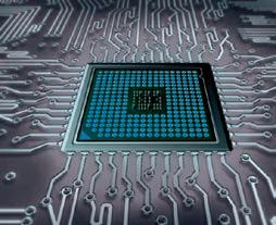
9. IC INTERCONNECTS
Multi-level metallizations including barrier layers, liners, plugs, planarization and ARC, e.g.Ti-TiN, Ti-Al alloy, TiN
Throughput up to 50 wafers/hour (Aligndegas- etch- 30nm Ti- 500nm Al- 150nm ARC TiN- cool)
4. 1. 8. 6. 7. 5. 3. 2.CLUSTERLINE® 3
9.
CLUSTERLINE® 200
Proven deposition processes for piezoelectrics, magnetic layers, metals and dielectrics
—
—
—
PLATFORM FEATURES –Dedicated solutions that give you the edge
From the modular chuck design for rapid exchange between 100,150 or 200mm formats to the twin high speed load locks or the Windows interface and SEMI SECS/ GEM compliant interface, CLUSTERLINE® 200 ensures maximum tool utilisation and full fab integration.
Auxiliary module functions including wafer alignment, degassing, cooling, six-slot buffer, DMC/ID reader.
Two load lock cassette stations with auto-home, featuring ergonomic loading, soft pump and soft vent, mapping functions to detect cross-slotted, double-loaded wafers, instant wafer slide out (protrusion) detection.
Modular chuck design for fast size and configuration conversion (4”, 5”, 6” and 8”).
100/150/200 bridge or split tool capability.
4
CHOOSE CLUSTERLINE® 200 FOR:
— LED
WIRELESS
— THIN FILM HEADS
MEMS
BACKSIDE METALLIZATION & THIN WAFER PROCESSING
CLUSTERLINE® 200 BRINGS YOU:
— PVD, high energy PVD, Soft Etch or PECVD process technologies on substrates up to 200mm
— Up to 6 Process Modules plus additional auxiliary modules for alignment, cool or degas, buffer or “in situ” metrology
— Direct thin wafer handling and processing capability for thicknesses down to 70μm and wafer bow up to 6mm
— Open system architecture, easily configurable and expandable
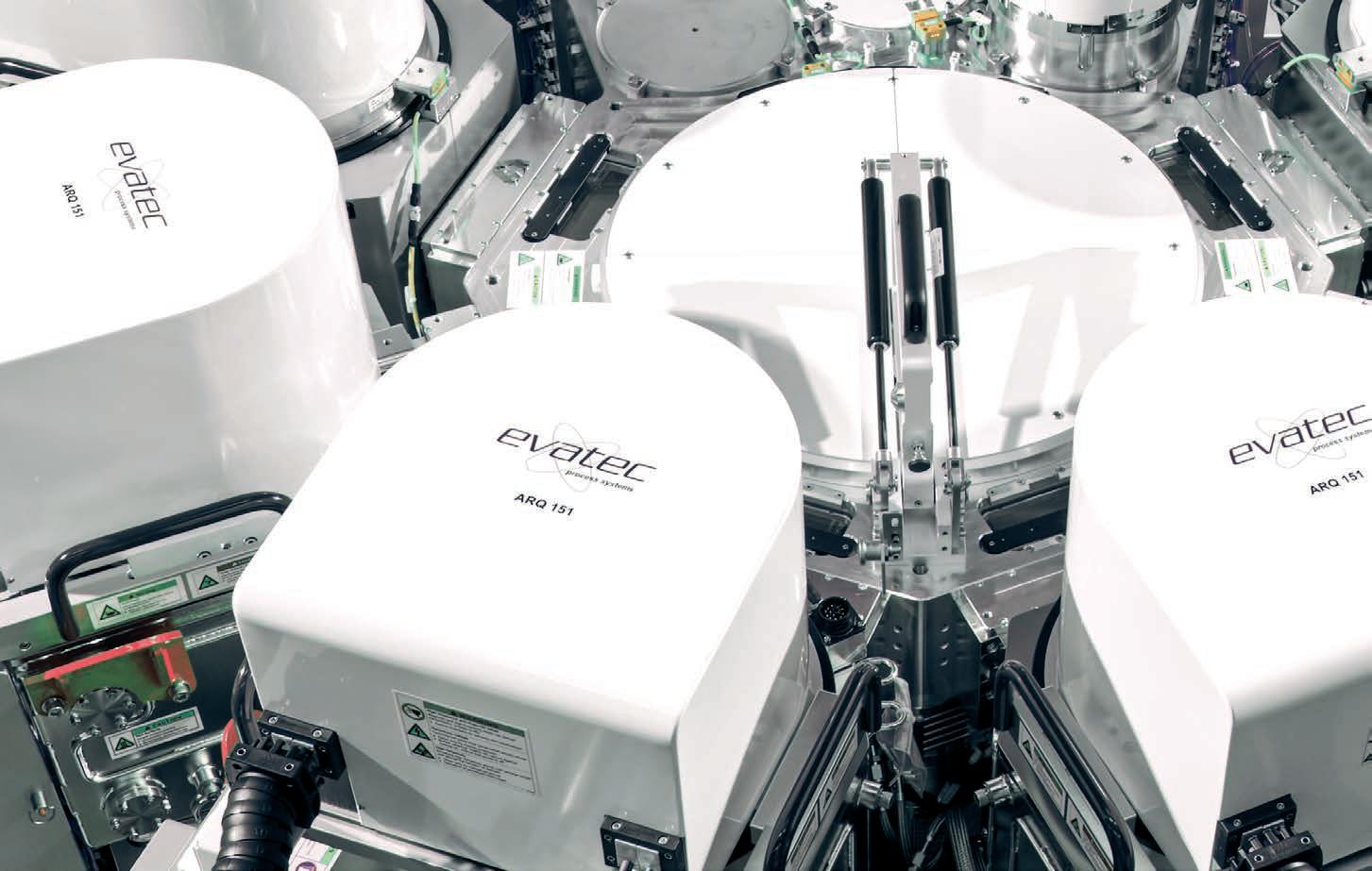
PROCESS MODULE CAPABILITIESA dedicated solution just for your application
Evatec offers a range of degas, etch and high uniformity deposition technologies with “in situ” Advanced Process Control (APC) capability that gives you the edge in throughput and yield. Ask our application engineers about a solution that’s just right for you.
— RF and DC planar magnetron sputter sources with specific magnet solutions for extremely high film uniformity and homogeneity and alignment of magnetic films.
Rapid degas and cool module for wafer conditioning and enhanced process throughput
ICP soft etch process module with MF Plasma enhanced RF Etch enabling high etch rate and excellent uniformity at low bias voltages. Reactive processing with H2 and O2 is available.
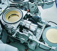
Multisource Quattro with rotating chuck (clamped/clamp less) with up to four sources on one module for single target or simultaneous co-sputtering using RF, DC or RF/DC superimposed sputtering.
PECVD process module featuring a separate reactor within the process chamber to provide enhanced uniformity, film purity and control of doping. “In situ” cleaning technology takes away the usual requirement for the frequent cleaning needed in standard reactors.
Highly ionized PVD source technology for high aspect ratio TSV applicationsmainly for 3D packaging and MEMS.
— Substrate chucks can be configured for either configured as ESC, clamp less or clamped setup using gas conduction for active wafer cooling or heating in PVD and or ICP soft etch modules. Chuck RF Bias is an option. Chuck temperatures controlled from -30°C up to 800°C, specific Carbon Heater solutions for up to 800°C (Sapphire) or 860°C ( Silicon) in the deposition of high performance AlN (NanoSmooth™ process) or PZT.
5 CLUSTERLINE®
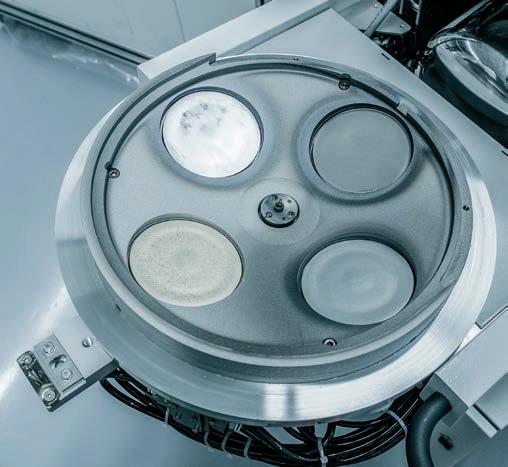
MSQ200 with 4 different targets
MSQ 200 with shutter installed
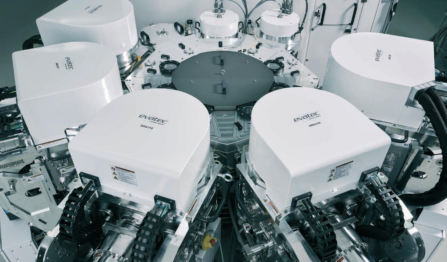
CLUSTERLINE® 300
UBM/RDL, TSV, Fanout and High Speed Backside Metallization Processes
CHOOSE CLUSTERLINE® 300 FOR:
— WAFER LEVEL PACKAGING
— BACKSIDE METALLIZATION & THIN WAFER PROCESSING
PLATFORM FEATURESAll the performance you need for Advanced Packaging and Backside Metallization processes
Building on the know how from CLUSTERLINE® 200, the 300mm tool integrates rapid atmospheric front end handling and advanced new process components for AP and BSM applications whilst retaining flexibility for 200mm wafer handling. Just like all the CLUSTERLINE® family, easy operating Windows based handling and SEMI SECS/GEM compliant interface come as standard.
High volume 300mm tool with Split or Bridge Tool capability for 200mm wafers.
Six dedicated SEMI standard interfaces for process modules, three configurable interface modules (either single or dual airlock configuration) for e.g. six slot buffer, cooler or degasser.
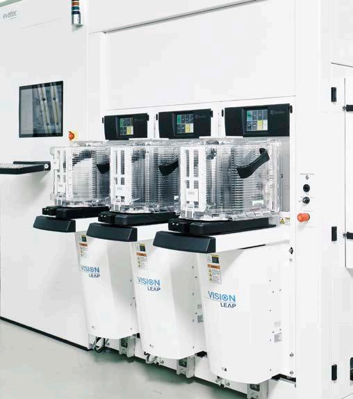
— Mini environment with 300mm FOUP load ports or open cassettes for 200mm.
ATMOSPHERIC FRONT ENDReliable handling each and every time in 24/7 production
Atmospheric front end handling in a Class 1 mini environment by four axis robot with standard options including heating or cooling, wafer inverter, active wafer centering and buffering means perfect delivery of each and every wafer in 24/7 production.
— BROOKS JCP AFEM with up to four FOUP load-port cassette stations, with mapping functions to detect cross-slotted, doubleloaded wafers, with instant wafer slide out (protrusion) detection at cassette stations.
Vision™ Load Port Modules with 300mm FOUP load ports or open cassettes for 200mm.
— Wafer aligner (RAZOR™) for rotational pre-alignment (0.3°) and centering of wafers (0.05mm).
Wafer flip station for back side metallization.
Buffer station for up to 12 wafers.
6
CLUSTERLINE® 300 BRINGS YOU:
— PVD, high energy PVD and soft etch process technologies on substrate sizes up to 300mm
PROCESS MODULES / COMPONENTSDedicated source technologies deliver high efficiency Rc and TSV metallization processes

The PVD module comes with either DC or pulsed DC sputter source with uniformity compensation over target life. Chuck tops are available either in metal or ceramized versions, and either with mechanical clamping, ESC with shadow mask and gas conduction back side heater/cooler for precise temperature control or clamp less chuck with shadow mask. Controlled chuck temperature is available from -30°C up to 500°C, optional chuck RF Bias. Suitable for reactive processing with N2 or O2
— ICP soft etch process module with MF Plasma enhanced RF Etch enabling high etch rate (SiO2 removal 0,6 – 0,8 nm/s) and excellent uniformity at low bias voltages. Reactive processing with H2 and O2 is available. For special heat treatment a separate hot chuck Degas Module or Radiation Degasser source is available.
High Pressure Degasser module (wafer at ~140°C in ~10sec with He up to 20mbar, max 180°C).
— Optimized configuration for organic/mold substrates which comes with Arctic metal cage (Ice Dome) and arctic chuck cooling down to -30°C, enabling highest kit life in the etch module for organic wafers like PI or PBO.
Atmospheric Batch Degasser integrated in AFEM with 44 slots allowing continuous degassing of advanced packaging substrates.
— Highly ionized PVD source technology for high aspect ratio TSV applications mainly for 3D packaging.
Multisource with rotating chuck - up to 4 RF or DC sources on one module for single target or simultaneous sputtering. Optional APC with fully integrated Pyrometer.
7 CLUSTERLINE®
— Direct thin wafer handling and processing capability for thicknesses down to 300μm and wafer bow up to 4mm
— “Arctic” dome and chuck capability for stable Rc processes on organic wafers PI/PBOProcess modules with easy access Atmospheric front end Proven wafer handling
CLUSTERLINE®
The CLUSTERLINE® series provides state-of-the-art process capabilities as well as extensive pre- and post-treatment steps. The open system architecture allows easy tool configuration for PVD, highly ionized PVD, and Soft Etch for wafer sizes up to 300mm.
ABOUT EVATEC
Evatec offers complete solutions for thin film deposition and etch in the Advanced Packaging, Power Devices, MEMS, Wireless Communication, Optoelectronics and Photonics markets.
Our technology portfolio includes a range of advanced sputter technologies, plasma deposition & etch as well as standard and enhanced evaporation.
Our team is ready to offer process advice, sampling services and custom engineering to meet our customers individual needs in platforms from R&D to prototyping and true mass production.
We provide sales and service through our global network of local offices. For more information visit our website at www.evatecnet.com or contact our head office.
TYPICAL LAYOUT - CLUSTERLINE® 300 TYPICAL LAYOUT - CLUSTERLINE® 200 3700 2900 4500 5300
Evatec AG Hauptstrasse 1a CH-9477 Trübbach Switzerland Tel: + 41 81 403 80 00 Fax: + 41 81
80
info@evatecnet.com www.evatecnet.com Product descriptions, photos and data are supplied within the brochure for general information only and may be superseded by any data contained within Evatec quotations, manuals or specifications. Edition 5 April 2023 (Edition 4: first printed December 2021,Edition 3 first printed Aug 2017, Edition 2 first printed Jan 2016, Edition 1 first printed Sep 2015). EVA_Brochure_CLUSTERLINE_FAMILY_Edition5_April2023
403
01