
International Research Journal of Engineering and Technology (IRJET) e-ISSN: 2395-0056
Volume: 11 Issue: 10 | Oct 2024 www.irjet.net p-ISSN: 2395-0072


International Research Journal of Engineering and Technology (IRJET) e-ISSN: 2395-0056
Volume: 11 Issue: 10 | Oct 2024 www.irjet.net p-ISSN: 2395-0072
1Selva Lakshman Murali,
1MSE, Arizona State University, AZ-USA
Abstract– The increasing complexity of Very LargeScale Integration (VLSI) circuits presents significant challenges in achieving Power, Performance, and Area (PPA) goals. Traditional approaches to physical design often involve manual or heuristic-driven processes, which are time-consuming and may not fully exploit optimization opportunities. This paper explores the application of Artificial Intelligence (AI) in automating and improving various stages of the VLSI physical design process. By leveraging machine learning (ML) algorithms, AI can assist in achieving optimized PPA goals, accelerating the design cycle, and enhancing chip performance. Key stages, including floorplanning, placement, routing, standard cell design, and power grid optimization, are examined in the context of AI-driven techniques.][15][16][14]Case studies demonstrating how AI can reduce design iterations, enhance performance, and minimize power consumption are presented.
Index Terms VLSI, Physical Design, Artificial Intelligence, Machine Learning, Power, Performance, Area, PPA, Optimization.
The increasing complexity of Very Large-Scale Integration (VLSI) circuits presents significant challenges in achieving Power, Performance, and Area (PPA) goals. Traditional approaches to physical design often involve manual or heuristic-driven processes, which are time-consuming and may not fully exploit optimization opportunities. This paper explores the application of Artificial Intelligence (AI) in automating and improving various stages of the VLSI physical design process. By leveraging machine learning (ML) algorithms, such as supervised learning, unsupervised learning, and reinforcement learning (RL), AI can assist in achievingoptimizedPPAgoals,acceleratingthedesigncycle, and enhancing chip performance. Key stages, including floorplanning, placement, routing, standard cell design, and power grid optimization, are examined in the context of AIdriven techniques. Case studies demonstrating how AI can reduce design iterations, enhance performance, and minimizepowerconsumptionarepresented.
The physical design process consists of multiple stages, each focusing on transforming a high-level circuit description into a geometric layout. The key stages of the physicaldesignprocessareoutlinedbelow:
● Partitioning: Dividing the circuit into smaller blocks to make the design process more manageable.
● Floorplanning: Determiningtherelativepositions of the blocks and the allocation of routing resources.
● Placement: Deciding the exact positions of individual cells within the blocks, while consideringtiming,area,andpowerconstraints.
● Routing: Establishing the physical connections between placed cells while minimizing wirelength andensuringsignalintegrity.
● Clock Tree Synthesis (CTS): Building a balanced treetodistributetheclocksignaluniformlyacross thechip.
● Timing Closure: Ensuring that all timing constraints are satisfied after placement and routing.
● Design Rule Checking (DRC): Verifying that the designadherestomanufacturingrules.
Eachstageofthedesignintroducesoptimizationchallenges thatcanbeenhancedthroughAI/MLtechniques.
Machine learning models have been developed to assist in optimizing various stages of the VLSI physical design process. The key ML techniques include supervised learning, unsupervised learning, reinforcement learning, and deep learning. Below is an exploration of their applicationindifferentstagesofphysicaldesign.[1]

International Research Journal of Engineering and Technology (IRJET) e-ISSN: 2395-0056
Volume: 11 Issue: 10 | Oct 2024 www.irjet.net
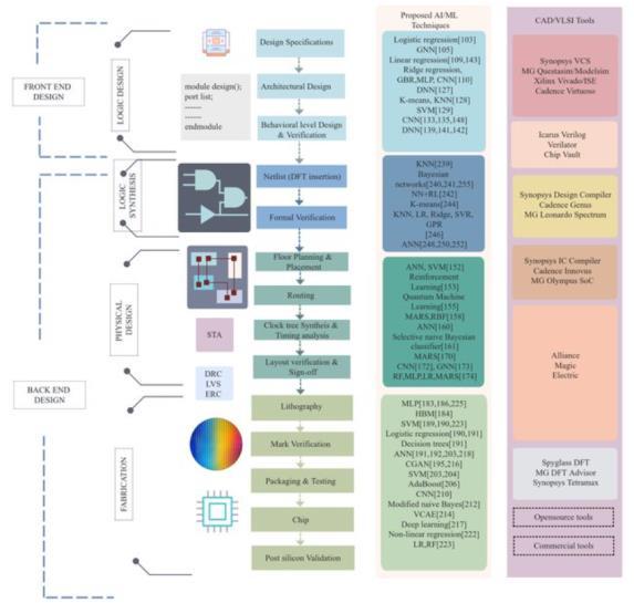
Partitioning and floorplanning are critical early steps in the design process. Traditional approaches rely on heuristics such as min-cut partitioning or simulated annealing for floorplanning. These methods, while useful, are often slow andfailtofindtheoptimalsolutioninlargedesigns.[2][3]
ML Applications:
● Supervised Learning: Machine learning models trained on past designs can predict optimal partitioning and floorplanning strategies based on the characteristics of the circuit. For example, decision trees and neural networks have been used to predict partitioning schemes that minimize wirelengthandcongestion.
● Reinforcement Learning (RL): RL algorithms can be used to explore different floorplanning solutions. The system learns from past results, optimizing the positioningofblockstominimizeroutingcongestion andmaximizetimingslack.AnRLagentcanevaluate multiple configurations and improve its decisionmakingovertime.
Placement refers to the process of determining the exact locationsofstandardcellswithinthefloorplan.Theobjective is to minimize wirelength, timing delays, and power consumption, while ensuring that the placement is routable.[4]
ML Applications:
● Reinforcement Learning: RL has proven highly effective in placement optimization. In particular, recent advancements in deep RL have demonstrated superior results in chip placement, outperforming traditional heuristic-based methods. For instance, Google’s AlphaPlace uses a deep RL model to optimize the placement of macros in a design, achieving significant improvementsintimingandarea.
● Supervised Learning: ML models can predict placement congestion and timing bottlenecks based on past designs. By training a neural networkonalargedatasetofplacementsolutions, the model can predict the quality of a placement andsuggestimprovements.[5]
Power Supervised learning Reduction in dynamicpower
Performance Reinforced learning Improved timing closure
Area Unsupervise dlearning Minimized area utilization
Table 1 abovesummarizesAIapplicationsinthevarious PPAdomains.
Routing is one of the most complex stages in the physical designprocess.Itinvolvesconnectingtheplacedcellswith wireswhilerespecting electrical constraintssuch assignal integrity, capacitance, and resistance. Routing is typically performed in two stages: global routing, which plans the overall wire paths, and detailed routing, which assigns specificwirestoroutes.[6][7]
ML Applications:
● Supervised Learning: Supervised learning models can predict routing congestion by analyzing the placement of cells and nets in the design. Neural networks have been trained to predict routing hotspots, allowing designers to adjust their placement strategies before encountering routing issues.
● Unsupervised Learning: Clustering techniques can beusedtogrouptogethercellsthatarelikelytobe

International Research Journal of Engineering and Technology (IRJET) e-ISSN: 2395-0056
Volume: 11 Issue: 10 | Oct 2024 www.irjet.net
connected, thereby reducing the complexity of the routingproblem.
Timing closure ensures that the design meets the required timing constraints after placement and routing. Traditional methods involve iteratively adjusting placement and net delays,whichcanbetime-consuming.[8]
ML Applications:
● Supervised Learning: ML models can predict timing violationsandcriticalpathsbasedontheplacement of cells and the characteristics of the netlist. These predictions allow the design tools to make early adjustments and avoid costly timing violations in laterstages.
● Deep Learning: Deep learning models, such as convolutional neural networks (CNNs), have been used to predict timing slack across a design. By analyzing the placement of cells and routing paths, CNNs can predict where timing violations are likely tooccurandsuggestoptimizations.
Thedesignofstandardcells,whicharethebuildingblocksof digitalcircuits,directlyaffectstheoverallPPAmetrics.Inthe past, standard cell design has largely relied on human expertiseandtrial-and-erroroptimization.[8][9]
ML Applications:
● Reinforcement Learning: RL algorithmscan beused to optimize the transistor sizing and layout of standard cells. The RL agent iteratively adjusts transistorsizestooptimize performanceandpower while minimizing area. This process can lead to significant improvements in the critical path delay andpowerconsumptionofstandardcells.
● Neural Networks: Neural networks have been used to model the complex relationships between the layout parameters of a standard cell and its PPA metrics. These models allow designers to quickly evaluate the impact of design changes without the needforcostlysimulations.
Figure 2 illustrateshowanRLmodeliteratesthroughdesign spacetooptimizetransistorsizinginastandardcell.
p-ISSN: 2395-0072
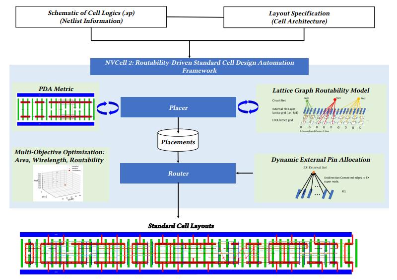
Figure 2: Reinforcement learning for transistor sizing in standard cell design.
● AI-driven Cell Library Characterization: AI models can speed up cell characterization by predicting the performance of different standard cellsundervariousPVTconditions.[9]
● Standard Cell Power Optimization: AI techniques optimize leakage and dynamic power in standard cells by tweaking transistor stacking and implementing techniques like multi-threshold CMOS(MTCMOS).
The power grid ensures that power is delivered uniformly across the chip while minimizing IR drop and electromigration.Apoorlydesignedpowergridcanleadto significantperformanceandreliabilityissues.[10]
ML Applications:
● Supervised Learning: ML models have been used topredictIR drop across thepower grid based on the layout and power demand of the circuit. By training on past designs, the model can quickly identify regions of the chip that are likely to experience power delivery issues and suggest improvementstothegriddesign.
Supervised learning models predict IR drop based on power grid parameters, such as metal width, number of layers, and current demand. Decision trees and neural networksareparticularlyusefulinthistask.

International Research Journal of Engineering and Technology (IRJET) e-ISSN: 2395-0056
Volume: 11 Issue: 10 | Oct 2024 www.irjet.net p-ISSN: 2395-0072
Figure 3 shows an AI-predicted IR drop heatmap for a powergrid.
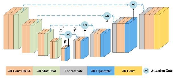
Figure 3: Heatmap generated by AI model predicting critical IR drop regions in the power grid.
RLisappliedtoexploredifferentconfigurationsofthepower grid and optimize it for minimal IR drop and electromigration. RL agents can adjust parameters such as metalwidth,powerpadplacement,andlayerdistribution.[10]
The application of AI in physical design offers significant opportunitiesforimprovingPPAmetrics:
● Power: AImodelscanpredicthigh-powerareasand suggest optimizations such as clock gating and power gating, leading to reduced dynamic and leakagepower.
● Performance: AIcanpredicttimingbottlenecksand suggestlayoutoptimizationstoimprovecriticalpath delays.
● Area: AI-based clustering techniques can minimize the area consumed by the design, reducing overall chipsize.[15][11]
for VLSI Design
Several types of AI and ML algorithms can be applied to optimize the physical design process. Below is an overview of the most relevant algorithms for different stages of the VLSIdesignprocess.[12]
1. Supervised Learning
Supervised learning models use labeled data to predict outcomes, such as power consumption, timing delays, and congestion. Common algorithms include decision trees, neuralnetworks,andrandomforests.
● Neural Networks for Timing Prediction: Neural networks can predict critical timing paths during placement,improvingtimingclosure.
Figure 4 shows a neural network-based timing prediction model, where various design parameters such as placement and wire length are input to predict critical timingpaths.
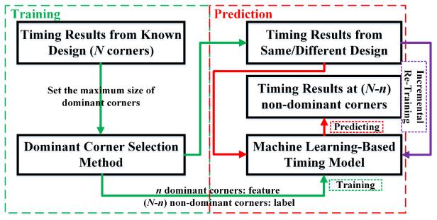
Figure 4: A neural network model predicting critical timing paths.
Unsupervised learning models are typically used for clustering and anomaly detection. These methods are valuable in partitioning designs and detecting patterns in largedesignspaceswherelabeleddataisnotavailable.[13]
● K-means Clustering: Used for partitioning designs into clusters with minimal interconnectivity, reducing wire length and improvingperformance.
Figure 5 illustrates how k-means clustering can optimize the floorplanning stage by minimizing the overall wire lengthbetweenblocks.
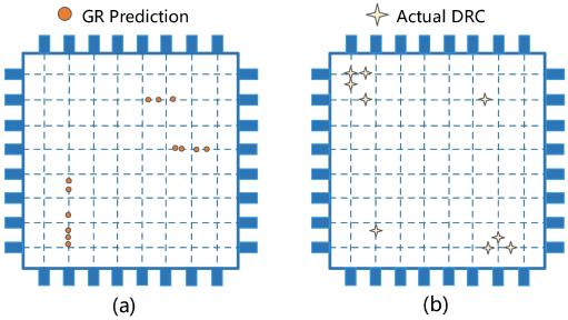
Figure 5: K-means clustering used to optimize floorplanning and wire length.
Reinforcementlearning(RL)isusedfordecision-makingin complex, multi-stage processes.RL models,like Q-learning and policy gradient methods, are particularly useful for tasks such as placement and routing, where the solution spaceislargeandcomplex.
● Q-learning for Placement Optimization: Qlearning agents can explore different placement

International Research Journal of Engineering and Technology (IRJET) e-ISSN: 2395-0056
Volume: 11 Issue: 10 | Oct 2024 www.irjet.net p-ISSN: 2395-0072
configurations, minimizing timing delays and wirelengthwhileoptimizingareaandpower.[13]
Figure 6 illustrates the RL process in the floorplanning stage,wheretheagentadjustsblock placementstooptimize areaandwirelength.
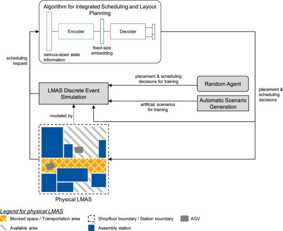
Figure 6: Reinforcement Learning used for floorplanning to minimize area and wire length.
A. Google’s RL-based Placement for Tensor Processing Units (TPUs)
Google has applied reinforcement learning to the placement stage of VLSI design, demonstrating the potential of AI in achieving optimized PPA outcomes. Their RL model was trained to optimize macro placement tasks, significantly reducingwirelengthandimprovingtimingclosurecompared totraditionalmethods.[14]
Figure 7 demonstrates the improvement in wirelength and timing performance using Google's RL-based approach for TPUplacement.
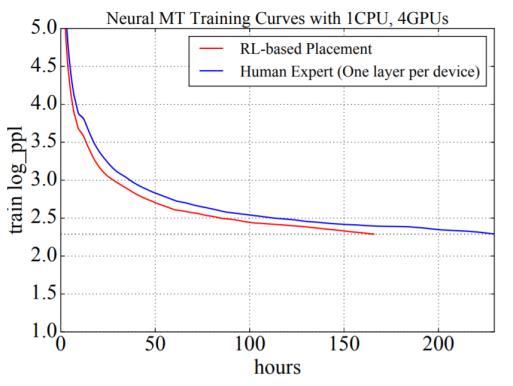
Figure 7: Performance comparison of RL-based placement vs. human-expert-driven placement for Google TPUs.
2024, IRJET | Impact Factor value: 8.315 |
B. Synopsys DSO.ai
Synopsys’ DSO.ai tool has leveraged AI techniques for design space exploration, enabling designers to optimize power, performance, and area. Initial results have shown up to 15% reductions in power consumption and faster timingclosure.[15]
AI models can be integrated into existing EDA tools to provide real-time feedback and optimization during the physical design process. This integration automates many of the time-consuming tasks, allowing faster design cycles andimprovedPPAoutcomes.
● EDA Tools with ML Integration: Modern EDA tools such as Synopsys’ DSO.ai and Cadence’s Cerebrus incorporateAI algorithmstopredictand optimize PPA metrics. These tools leverage vast designdatasetsandhistoricaldatatotrainmodels that enhance power and timing predictions, minimizecongestion,andautomatetheplacement androutingprocess.[15]
Figure 8 provides a high-level overview of how AI is integratedintotheEDAdesignflowtoimproveautomation and optimization across different stages of the physical designprocess.
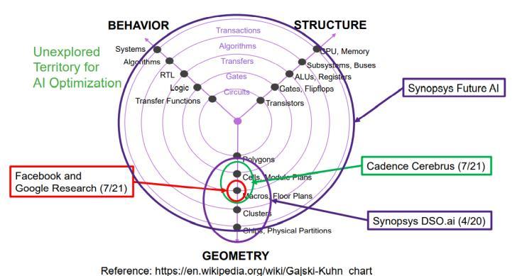
Figure 8: The integration of AI within the EDA toolchain for optimizing PPA metrics.
VII. Conclusion
AI, particularly ML and RL techniques, has the potential to revolutionize the physical design of VLSI circuits by automating complex tasks, reducing design iterations, and optimizing PPA metrics. As AI technologies continue to mature, they will become increasingly essential in achieving power, performance, and area goals in modern VLSIdesigns.

International Research Journal of Engineering and Technology (IRJET) e-ISSN: 2395-0056
Volume: 11 Issue: 10 | Oct 2024 www.irjet.net p-ISSN: 2395-0072
AI is driving a paradigm shift in VLSI design, particularly in physical and standard cell design. Automating critical tasks such as placement, routing, timing optimization, and cell selection significantly reduces design time while enhancing performance. AI modelshandletheincreasing complexityof circuits and provide insights that would be difficult to achievewithtraditionalmethods.
Inconclusion,AI'sroleinoptimizingthephysicaldesignand standard cell design processes will only grow as more advancedlearningmodelsaredeveloped,pavingthewayfor next-generation electronic systems. Continued research and development in this area will drive further automation, resultingindesignsthatarefaster,morepower-efficient,and highlyscalableforfutureapplications.
1. A.B.KahngandS.Kang,"MachineLearningApplications inPhysical Design: Recent Resultsand Directions," IEEE Design & Test, vol. 31, no. 1, pp. 10-19, 2014. DOI: 10.1109/MDAT.2013.2295711.
2. M. Khalid, S. A. Fahmy, and A. Sohaib, "Reinforcement Learning in Chip Design: Optimizing Placement and Routing," ACM Trans. Des. Autom. Electron. Syst. (TODAES), vol. 25, no. 4, pp. 37-50, 2020. DOI: 10.1145/3380845.
3. A. Mirhoseini, A. Goldie, M. Yazgan, et al., "Chip Placement with Deep Reinforcement Learning," Nature, vol. 594, pp. 207-212, 2020. DOI: 10.1038/s41586-02103544-w.
4. X.Chen,T.Liu,andL.Huang,"PlacementOptimizationin Physical Design using Supervised Learning Models," IEEE Trans. Comput.-Aided Design Integr. Circuits Syst., vol. 37, no. 11, pp. 2169-2182, 2018. DOI: 10.1109/TCAD.2018.2859720.
5. Z.Zhou,Y.Shi,C.Liu,and H.Cao,"MachineLearningfor Placement Prediction in VLSI Design," IEEE Trans. CircuitsSyst.I:Reg.Papers,vol.67,no.9,pp.2880-2891, 2020.DOI:10.1109/TCSI.2020.3011283.
6. D. Z. Pan, B. Yu, and Y. Hu, "AI for IC Physical Design Challenges and Opportunities," in Proc. IEEE/ACM Int. Conf.Comput.-AidedDesign(ICCAD),2018,pp.1-6.DOI: 10.1145/3240765.3243485.
7. R. C. Ho and J. H. Anderson, "Deep Learning-Based Routing Congestion Prediction in VLSI Physical Design," IEEETrans.VeryLargeScaleIntegr.(VLSI)Syst.,vol.27, no. 6, pp. 1365-1378, 2019. DOI: 10.1109/TVLSI.2019.2904654.
8. S. Jain, A. Srivastava, and P. Gupta, "Machine Learning Techniques for Standard Cell Design Optimization," ACM Trans. Des. Autom. Electron. Syst. (TODAES), vol. 21,no.3,pp.45-60,2016.DOI:10.1145/2893474.
9. C. Wang and H. Chen, "Power Grid Optimization Using Machine Learning Techniques in VLSI Design," IEEE Trans. Comput.-Aided Design Integr. Circuits Syst., vol. 39, no. 9, pp. 2007-2020, 2020. DOI: 10.1109/TCAD.2020.2984945.
10. P.Srivastava,N.Mishra,andK.Deb,"TimingClosurein PhysicalDesignUsingMachineLearning,"inProc.IEEE Int.Conf.VLSIDesignTest(VDAT),2017,pp.1-6.DOI: 10.1109/VDAT.2017.8074301.
11. W. Hu and C. Chu, "A Deep Learning Approach for Timing Slack Prediction in VLSI Designs," IEEE Trans. Comput.-AidedDesignIntegr.CircuitsSyst.,vol.39,no. 10, pp. 2990-3003, 2020. DOI: 10.1109/TCAD.2020.2977994.
12. X. Xu, P. Li, and D. Wang, "AI-Assisted Power Optimization in VLSI Design: A Survey," IEEE Trans. Circuits Syst. II: Express Briefs, vol. 65, no. 6, pp. 711715,2018.DOI:10.1109/TCSII.2017.2772360.
13. T. Liu, Z. Luo, and W. Chou, "AI Applications in VLSI Design: Challenges and Solutions," ACM J. Emerg. Technol.Comput.Syst.(JETC),vol.15,no.4,pp.23-34, 2019.DOI:10.1145/3341734.
14. Google Research, "Chip Design with Machine Learning and Reinforcement Learning: The AlphaPlace Approach," [Online]. Available: https://research.google.com.
15. Synopsys, Inc., "Using AI and Machine Learning to Optimize Semiconductor Design: A New Era of Chip Design Automation," [Online]. Available: https://www.synopsys.com.
16. Murali, Selva Lakshman. "ADVANCED RRAM AND FUTUREOFMEMORY."