
International Research Journal of Engineering and Technology (IRJET) e-ISSN:2395-0056
Volume: 11 Issue: 06 | Jun 2024 www.irjet.net p-ISSN:2395-0072


International Research Journal of Engineering and Technology (IRJET) e-ISSN:2395-0056
Volume: 11 Issue: 06 | Jun 2024 www.irjet.net p-ISSN:2395-0072
Selva Lakshman Murali, Arizona State University
Abstract Vertical Tunnel Field Effect Transistors (VTFET) has a different working principle than traditional FET’sandaresaidtobemorebeneficialthanthetraditional FinFETs that we have been using for decades. This paper presentsanewdevicearchitecture,whichcanbesharedby a wide range of sorts of semiconductor transistors. Here, the significance and prerequisites of the vertical transistor in the VLSI industry alongside its device processing have been illustrated. It moreover talked about the benefits and applications in memory, logic technology alongside analog developmentoverpastyears.Verticalsemiconductorshave helped decrease expenses per bit for flash memory and it has assisted with diminishing the leakage current in most recent innovation hubs. Looking for better performing devices specialists are presently investigating 3D designs, for example, vertical semiconductors, whose benefits incorporate low power consumption, smaller current leakage towards the bulk, and better suitability for adaptablehardware.
Keywords: Vertical Tunnel Field Effect Transistor (VTFET), atomic layer affidavit (ALD), Silicon-On-Insulator (Sal), gate-all-around (GAA), 3D designs, Memory application.
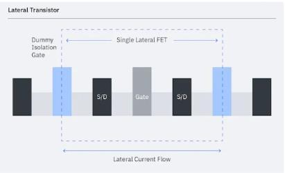
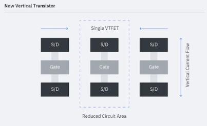
Modern electronics are mostly flat, with millions of planar silicon transistors lying on a chip’s surface. These aregettingfasterandefficienteverydaybecauseofthetiny chips that power these electronics evolving at an unprecedented rate. Our understanding at transistors or chipsstartswithatermcalledMoore’sLaw.Thislawstates thatthenumberoftransistorsonachipdoubleaboutevery twoyears.Thespeedofthechipdependsonthenumberof transistors on the chip. As the number of transistors keep on increasing year by year, we should now be worried about running out of space on the chip. One solution to overcome this problem is, to find a new technology where space is not the constraint, VerticalTransport Field Effect Transistors. This is a new technology to overcome the problem with the traditional MOSFET’s. In VerticalTransport Field Effect Transistors (VTFET), the transistors are arranged perpendicular to the plane of the chip. This eliminatesthespaceconstraintandallowstheengineersto pack a lot more transistors vertically in a given space. The VTFET’s are said to dominate the speeds of traditional FinFET’s. The transistors that we currently use has three terminals on the same plane: gate, source & drain. When a small voltage is applied to the gate terminal, the transistor will turn on and the current flows from source to drain. When these transistors are placed on the chip, there is a
veryhighchancethattheadjacenttransistorsinterfereeach other. To prevent them from interfering, we place dummy gatesbetweenthetransistorswhichoccupiesadditionalarea on the chip. VTFET’s does not need these dummy gates between them – they instead use something called as shallow trench isolation which doesn’t require any additional space on the chip. The current in VTFET’s also changes it direction from the traditional FinFET’s, which is perpendicular to the surface of the chip. This gives us the flexibility to change the length of the gate to control the current. toas"16/14," butreal "7nm" node circuitdensities will necessitate the next generation of lithography, EUV at 13.5nmwavelength.Thecostofthechip,whichischallenged by the requirement for unique cost-intensive patterning techniques,isthekeytoacceptanceintheelectronicsdevice area. Given the higher wiring parasitic, theability to gain more performance at constant chip power willbe the key to adoption in the server area. To get to mature 7nm nodes, new materials will be required in all scenarios.[3]

International Research Journal of Engineering and Technology (IRJET) e-ISSN:2395-0056
Volume: 11 Issue: 06 | Jun 2024 www.irjet.net p-ISSN:2395-0072
InaresearchperformedbyIBM,itisobservedthat the VTFET’s can allow up to five times more transistors on the chip of the same size. They also observed that there is a reduction in the capacitance and resistance, whichreducedthepowerinVTFET’s.
Proceeding with endeavors in Complementary Metal Oxide Semiconductor (CMOS) research have led to the remarkable increment of device integration density during the last 40 years. In the recent past increasing fabrication costs and increasing overall variability have turned into a hindrance for the scaling pattern. To beat suchlimits,impressiveexaminationisdevotedforinstance totheuseofnewmaterials(suchashigh-xdielectricswith metal gates), dual-gate devices, novel isolation techniques that make use of Silicon-On-Nothing (SON) or Silicon-OnInsulator(Sal)substrates[1].TheverticalFETofthefigure. 3wasfirstdeliveredbygateandetch-backmethodology.A n+Si(111)(~0,002ωcm)substratewasutilizedforvertical FET structure and a p+ Si(111) (ρ ~ 0.04 Ωcm) substrate wasutilizedforsteepSSswitchapplication.Thegateoxide was produced using 1ML-Al2O3/4 ML-HfO2 by the atomic layeraffidavit(ALD)andthethicknesswas4-14nm.Then, tungsten (W) was saved as a RF faltering metal gate. W is lithographically portrayed in NW-designed veils (50 × 50 μm2)andtheNWswerethencoveredbybenzocyclobutene (BCB)andcoveredbyreceptiveparticledrawing(RIE)with CF4/O2 mixed gas to draw BCB, W, and HfALO gate oxide constantly.[4][5] After the RIE, the NWs had been encased by the BCB and scaled back by the RIE to oblige the metal gate and pipe. By then, Ni/Ge/Au/Ni/Au vanished into a lithographically described locale as a channel link for the InGaAs nanowire-net. Over the long haul, the NW-SGT was temperedat420ºCinN2includingtheacquisitionofOhmic contacts in the source / channel region as a post metallizationsteptoreinforcethegateoxide.
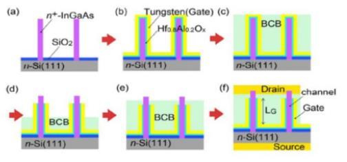
Fig. 3. Device fabrication processes: (a) InGaAs NW growth. (b) Atomic layer deposition of Hf0.8Al0.2Ox and sputtering of W-gate metal. (c) Spin-coating of BCB polymer. (d) RIE of BCB, gate oxide and W metal. (e) Spincoating of BCB and RIE etch back for electrical separation layerformation.(f)Drainandsourcemetalevaporation
VTFET technology will impact memory technologies and could potentially replace DRAM’s with SRAM’s. We know
that DRAM is a cheap memory technology which stores the data using a capacitor. But SRAM’s are comparatively faster than DRAM’s which does not require refresh cycles as the data isnon destructivei.edoesnot requirea writeback.But the capacitor which is used to store data in DRAM needs to berefreshedatregularintervalstoholdthedatain itunlike SRAM.Ifthedependencyon thiscapacitoriseliminated, the memory can be made more scalable. Capacitor less 1TDRAMs are receiving increasing attention for memory applications due to the integration limitations of conventional single capacitor DRAMs in nanoscale CMOS technologies.[7] [8] So the vertical transistors comes in to picturetoimprovethisscalabilitythatthetraditionalDRAM is seeing.The trench capacitance in the vertical transistors canreplacethecapacitorthatispresentintheDRAMwhich willalsohelpimprovetheretentiontimeofthememory.The trench structure reduces the electron-hole recombination. With the valence band offset between GaP and Si, holes can be confined in the storage region for improved retention times.AsVTFETsusestrenchesstructures,eliminatingholes isverytoughasthevoltagesrequiredtobiassuchdevicesis very large. This large biasing voltages will generate large currents in the device which directly relates to increase in power consumption. There are few papers which discussed howthispowerconsumptioncanbereducedsignificantlyby using alternate methods where the operating current in the deviceisreducedforlowpowerapplications.[2]
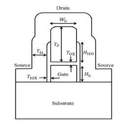
Fig.4showstheschematicoftheDRAMthatisimplemented using a type of vertical transistor i.e body over gate vertical nanosheet transistor. This device has a 3-wide source contact and one contact for the drain terminal. A significant amount of drain current is generated when the drain is positively biased. The write operation in this DRAM is controlledbytheionizationbetweenn-typechannelandthe ptype body. This ionization effect can be seen in the Fig. 5. With the help of positive drain bias voltage, the holes were forced to the p-type body which reduces the threshold voltage by accumulating the excess carriers in the storage region.Becauseofthis,thereadingcurrentwillincrease.[6]

International Research Journal of Engineering and Technology (IRJET) e-ISSN:2395-0056
Volume: 11 Issue: 06 | Jun 2024 www.irjet.net p-ISSN:2395-0072
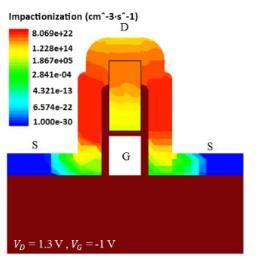
Fig.5.ImpactIonizations
Withthehelpofthispositivedrainbiasvoltage,theholes will be pushed into the storage region which can be retained in the p-type body with the help of negative gate bias voltage. SO holding the value 1 has a very high state density.Incontrast,holding 0will havealowholedensity. This can done by forward biasing the device which will then expel the holes from the storage region. This is how thedateisstoredinthedevice.
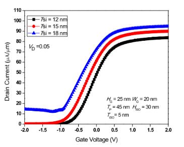
Fig.6.IVCharacteristicswithdifferentchannellayer thickness
Fig.6showsthe IVcharacteristicsof the device when the layer thickness of the channel is varied. This figure illustrates how the channel layer thickness impacts the input characteristics. The channel layer thickness can be controlledbycontrollingthegatevoltage.Thisimpactsthe programming window when the width of the channel is made too thick or too thin. So the thickness has to be optimized such that the programming window is not affected. From the figure we can also observe that the leakagecurrentisincreasingwhenthechannelthicknessis increased. So we should also make sure that the leakage current is not too large by selecting the optimal channel layerthickness.Sofromthe above plot,wecanseethat the
red curve is optimal with normal leakage current when compared to the other 2 curves. The programming window also depends on the isolation heights. This improves as isolation height is lowered since there are wider drain-end regions, which help to collect and store holes generated by theimpactionizationsimplybyusingnegativegatebias.Soit is better to maintain the drain-end regions as wide as possible so that it will allow the memory to write 1s and 0s efficiently.[9]
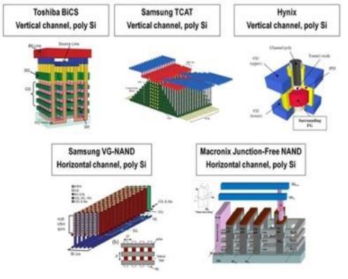
Significance of the Flash memory can be featured in numerousways.NAND/NORflashisquitepossiblythemain use of vertical transistors. Flash memory is a non-volatile memorychipusedforcapacityandformovingdatabetween a(PC)andcomputerizeddevices.Ittendstobeelectronically programmed and erased. EEPROM is a sort of data memory device using an electronic charge to eradicate or compose advanced information. Drifting gate transistors are electrically separated and utilize a coasting node in direct current (DC). A remarkable charge trap mechanism is utilizedtostoretheinformationanditsvaluereliesonlimit voltagewhichcanbechanged.[11]
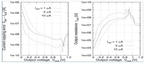
Fig.7.CurrentmirrorwiththeVeSFET-basedOTAinthe feedbackloop:(a)currentcopyingerrorand(b)output resistance.
3D NAND has ascended as a strong substitution to 2D NAND giving the continued scaling carried forward by extending the number of layers just as utilizing the prevalent cell attributes of the 3D NAND to build the quantity of bits/cell from 3 bits/cell to 4bits/cell. Many organizations, for example, Intel, WDC, Micron have been working on increasing the number of bits they want to store in the given area. A single cell can be used to save 2/4/8/16 bit value contingent on its order as TLC, QLC, MLC, and so on. This can be accomplished however the morenumberofbitstobestored,themorenumberofVth state should be characterized and this comes at the expenseofprecision.
NOR flash is generally faster to read than NAND flash , yetitislogicallyexpensive,andittakesmoretimetodelete and compose updated information. NAND has a higher storage bits limit than NOR. Alternately, equivalent NOR Flashmemorysupportsonebyteinconsistentaccess,which

Volume: 11 Issue: 06 | Jun 2024 www.irjet.net
engages machine rules to be recovered and run straightforwardly from the chip, correspondingly as a traditional PC recovers directions legitimately from the primarymemory.Nevertheless,NORmustwriteinbigger lumps called pages (bits) of data at once than NAND. parallel NOR Flash consists of a static random access memory (SRAM) interface that incorporates sufficient location pins to delineate the whole chip, empowering accesstoeachbyteinsideit
The Vertical Slit-based Field-Effect Transistor (VeSFET) is a clever junction-less device with two undefined, independently controlled doors. VeSTIC (Vertical-SlitSemiconductorBasedIntegratedCircuit)isa lately showed development for low-power VLSI circuits. ThecircuitsaremadewithaninsignificantlychangedSOI CMOS process course of action. Lithography necessities are essentially relaxed by the all out departure from the normalrectangularelementsinfavorofcircularonesand by incredible consistency of the design: all the devices, having the similar calculation, are separated on a square structure.ExpectedasanoptionincontrasttoCMOS,the advancement permits a basic mix of various sorts of device (double door MOSFETs, JFETs, and bipolar semiconductors) on a similar SOI wafer. The key properties of this device incorporates 1) Activity subject to the movement of majority carriers. Thus, the overwhelming system is incomplete consumption of the dynamic area as opposed to reversal. 2) Two undefined, independentlycontrolledgatesoneithersideoftheactive regionassociatingthesourceanddrain.Thecentral,most secure piece of the active region is insinuated as the slit The strong cross-fragment of the cut (and, subsequently, itsconductance)isobligedbythedevelopmentofdrained areasobligedbythevoltagesofthegates.
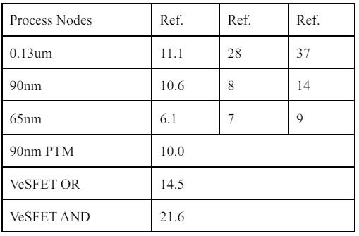
This table shows intrinsic voltage gain of the VeSFET compared to the MOSFET at different process nodes. The values of the above parameters propose that the VeSFET is superior to the MOSFET of the corresponding process node. A model use of the VeSFET based OTA is a high-precision current mirror. The best benefitoftheVeSFET, bethatasitmay,isthepresence of twoindependentgatescontrollingacommonchannel.The result voltage of this mirror is allowed to drop well beneath the immersion voltage of Mm2 in light of the fact that the current duplicating precision is ensured by identicaloperatingconditionsofbothtransistors.[9]
Strangely, the impact of the most striking vertical MOS unequivocal features like diverse source/drain designing, channel direction, and vertical gate oxide thickness on unwavering quality is examined. In spite of the way that LDD is missing, it is shown that cut back vertical semiconductors have a sufficient unwavering qualityforpossibleuseingigascalerecollections.[10][11]
DRAM working consists of four operating states. Thesestatesare:Reading,Writing,Holding,Erasing.Each stateconsumessomepowerandthispowerisdifferentfor different states. In one of the IEEE papers, the power consumption for all these four states are discussed clearly anditisfoundoutwhichstateconsumesthehighestpower and which consumes the least power. The power consumption in the erasing state is too low when compared to other states. In contrast, it is found out that the writing states consumes the highest amount of power. In this paper, they did not consider the power consumption of the holding state. This is because, in the holding state the current flowing through the device is negligible i.e almost 0. So this holding state power consumption is not included for the comparison. One important factor to consider here is the work function. When the work function is increased, the input characteristiccurvesareshiftedtotheright.Thisindicates that the gate voltage is being increased when the work function is increased. When the gate voltage is increased more and more, the operating current in the device is decreased which will directly lead to low power

International Research Journal of Engineering and Technology (IRJET) e-ISSN:2395-0056
Volume: 11 Issue: 06 | Jun 2024 www.irjet.net p-ISSN:2395-0072
consumption.Sotheworkfunctionisanimportantfactor whichwillhelpustodesignalowpowermemorydevice. In this paper, with the help of simulations, it is observed that the power consumption is reduced by 20.5% when the work function is increased while writing 1 in to the device. The power consumption is reduced by 24.6% when reading 1 and 75% while reading 0. It is observed that the most power is consumed when weare writing 1 to this device. So it is very important for a low power memory device to reduce the power consumed during thiswritingstate.[11][12]
Applications for the analog/RF and logic circuits have alsobeendiscussedandverticaltransistorscangiveupto 78% of area decrease in memory cells and has ended up being helpful in numerous other analog and logical applications. 3D heterogeneous compromise and heterogeneous structures are plausible responses to guarantee consistent advances in CMOS ICs as Moore's Law is wrapping up. Vertical semiconductor applications have conveyed various progressions alongside the difficulties in recent times. It has contributed towards betterlimitsallthroughthelatestcoupleofyears.[12]
We have discussed what challenges are we seeing in the memory’s. An important factor which can help reduce the power consumption in the memory device is discussed in this paper. By the simulations resultsdiscussedinpapers,wehaveseenhowthepower consumption is varied for different operating states. By adjustingtheworkfunction,wehaveseenhowthepower consumptioninthedeviceisreducedfor differentstates. Thiscanbeusedinthelowpowerapplications.
[1] A. Pal, K. C. Saraswat, A. Nainani, Z. Ye, X. Bao and E. Sanchez,”GaPsource-drainverticaltransistoronbulk silicon for 1-transistor DRAM application,” 2013 5th IEEEInternationalMemoryWorkshop,2013,pp.192195,doi:10.1109/IMW.2013.6582132.
[2] T. K. Agarwal, O. Badami, S. Ganguly, S. Mahapatra and D. Saha, ”Design optimization of gate-all-around vertical nanowire transistors for future memory applications,” 2013 IEEE International Conference of ElectronDevicesandSolid-stateCircuits,2013,pp.12,doi:10.1109/EDSSC.2013.6628113.
[3] Z. Fang et al., ”Fully CMOS-Compatible 1T1R IntegrationofVerticalNanopillarGAATransistorand Oxide-Based RRAM Cell for HighDensity Nonvolatile Memory Application,” in IEEE Transactions on ElectronDevices,vol.60,no.3,pp.1108-1113,March 2013,doi:10.1109/TED.2013.2240389.
[4] S. Mookerjea et al., ”Experimental demonstration of 100nmchannellengthIn0.53Ga0.47As-basedvertical
inter-band tunnel field effect transistors (TFETs) for ultra low-power logic and SRAM applications,” 2009 IEEE International Electron Devices Meeting (IEDM), 2009,pp.1-3,doi:10.1109/IEDM.2009.5424355.
[5] J. -T. Lin et al., ”Vertical Transistor With n-Bridge and BodyonGateforLow-Power1T-DRAMApplication,”in IEEETransactionsonElectronDevices,vol.64, no. 12, pp. 4937-4945, Dec. 2017, doi: 10.1109/TED.2017.2766563.
[6] J. Sim, M. Imani, Y. Kim and T. Rosing, "Enabling efficient system design using vertical nanowire transistor current mode logic," 2017 IFIP/IEEE International Conference on Very Large Scale Integration (VLSI-SoC), 2017, pp. 1-6, doi: 10.1109/VLSI-SoC.2017.8203486.
[7] E . Gn an i, S. Reggiani , M . Rudan, and G . Bacca rani, "Design Considerations and Comparative Invest igat ion of Ultra-Thin SO l , Double-Gate and Cylindrical Nanowire FETs," ESSDERC 2006, pp. 371-374, Sept. 2006
[8] L. Barbut, D. Bouvet and J. Sallese, "Towards fabrication of Vertical Slit Field Effect Transistor (VeSFET) as new device for nano-scale CMOS technology," CAS 2011 Proceedings (2011 International Semiconductor Conference), 2011, pp. 325-328,doi:10.1109/SMICND.2011.6095805.
[9] Electron Devices, vol. 67, no. 11, pp. 4626-4630, Nov. 2020,doi:10.1109/TED.2020.3020779.
[10] “Vertical Slit FET at7-nm Node and Beyond”, Ping-Lin Yang,StudentMember,IEEE,TerenceB.Hook,PhilipJ. Oldiges,SeniorMember,IEEE,andBruceB.Doris
[11] “Integration of III-V nanowires on Si: From highperformance vertical FET to steepslope switch” Katsuhiro Tomioka, Masatoshi Yoshimura, Eiji Nakai, FumiyaIshizakaandTakashi.